Dielectric constant of MgO tunnel barrier with epitaxial strain

Introduction
Spintronics-based devices utilize the spin degree of freedom and have unique features such as nonvolatility, low power consumption, infinite endurance, and compatibility with CMOS-based technology. The demand for applications of spintronics, such as magnetic sensors and magnetoresistive random access memory (MRAM) is growing rapidly. Magnetic tunnel junctions (MTJs) based on MgO tunnel barriers are key components of spintronics and have been widely used in these applications1,2. Recently, the voltage-controlled magnetic anisotropy (VCMA) effect3,4,5,6,7 has attracted attention as a technology to realize low-power spintronics devices such as voltage-controlled MRAM6,7,8. The VCMA effect was first demonstrated in a 3 d transition metal ferromagnetic layer using a liquid electrolyte3; it was then demonstrated in an all-solid structure with a MgO tunnel barrier9,10. Currently, structures that use an MgO tunnel barrier as the dielectric layer are the main focus of research on the VCMA effect. However, further enhancement of the VCMA effect is necessary for device applications; this has motivated attempts to incorporate high-k dielectrics as tunnel barriers to obtain greater charge accumulation and thus an enhanced VCMA effect. To date, MgO/HfO211,12,13, MgO/Pb(ZrxTi1-x)O3/MgO14, SrTiO315,16, and MgO/ZrO2/MgO17 have been used as the high-k dielectrics. We experimentally demonstrated the enhancement of the VCMA coefficient through the enhancement of dielectric constant εr by establishing a technique to derive εr for thin and small tunnel barriers13. However, research on the εr of tunnel barriers in MTJs is still in the early stages. Even for the MgO tunnel barrier, which has been investigated most intensively, εr has not been measured experimentally, and was assumed to be equal to the bulk value. Moreover, we recently reported a large εr for the MgO tunnel barrier in an epitaxial MTJ17; however, the origin of this phenomenon has not yet been elucidated.
In this study, we investigated the εr of the MgO tunnel barrier in epitaxial stacks with varying MgO thicknesses. We reproduced a large εr for the MgO tunnel barrier in the epitaxial stack and observed a trend of increasing εr with decreasing MgO thickness. We interpreted this trend in terms of the epitaxial strain. We also confirmed that variation of εr directly affects the VCMA coefficient.
Methods
Multilayered epitaxial stacks consisting of MgO (0 or 5 nm)/Cr (50 nm)/Fe (tFe nm)/Ir (0.06 nm)/Co (0.1 nm)/MgO (tMgO nm)/top electrodes were deposited on single-crystal MgO(001) substrates using a combination of molecular beam epitaxy (MBE) and magnetron sputtering techniques (Fig. 1a). Prior to deposition, the MgO substrate was cleaned by in situ annealing at 800 °C. The 5-nm-thick MgO seed layer was grown at 200 °C. The 50-nm-thick Cr buffer layer was grown at 200 °C by electron-beam evaporation or at room temperature (RT) by sputtering, followed by in situ annealing at 800 °C. Ultrathin Fe/Ir/Co layers were deposited at 150 °C, followed by in situ annealing at 250 °C. The MgO tunnel barrier was then deposited at RT and annealed in situ at 250 °C. Then, Cr (1 nm)/Pt (5 nm) or Pt (5 nm) cap layers were sputter-deposited on the MgO tunnel barrier at RT (MOKE stack) to evaluate the magnetic properties by vibrating sample magnetometry (VSM) and magneto-optical Kerr effect (MOKE), while a Fe (10 nm) reference layer and Ta (5 nm)/Ru (7 nm) cap layers were deposited by electron-beam evaporation and sputtering, respectively (MTJ stack), to measure the tunnel magnetoresistance (TMR) effect. Layers other than Cr, Pt, Ru, and Ta were deposited by electron-beam evaporation in the MBE chamber. For comparison, we also prepared a polycrystalline stack composed of Ta (5 nm)/Ru (10 nm)/Ta (5 nm)/Fe80B20 (tFeB nm)/MgO (tMgO nm)/top electrode on a thermally oxidized Si substrate. Prior to deposition, the thermally oxidized Si substrate was cleaned by in situ annealing at 400 °C. The Ta/Ru/Ta/Fe80B20 layers were deposited by sputtering at RT, while the MgO layer was deposited by electron-beam evaporation at RT, followed by in situ annealing at 260 °C. On the MgO tunnel barrier, Cr (1 nm)/Pt (5 nm) cap layers were sputter-deposited at RT (MOKE stack) to evaluate the magnetic properties, while Fe80B20 (10 nm)/Ta (5 nm)/Ru (7 nm) layers were sputter-deposited (MTJ stack) to measure the TMR effect. The method for the preparation of a similar polycrystalline stack was described in our previous study13. The sample was microfabricated into pillars and used for the capacitance, MOKE, and TMR measurements. We microfabricated pillars (devices) of multiple sizes (S) on one sample: devices with S = 36, 64, 100, and 144 μm2 (MOKE device) or S = 22.5, 30, 62.5, and 90 μm2 (MTJ device) were used for size-dependent capacitance measurements; S = 80 μm2 was used for the MOKE measurements; and S = 10 μm2 was used for the TMR measurements. For accurate evaluation of εr, we used relatively large device sizes. We note that the capacitance and MOKE or TMR measurements were performed for the same sample but different devices.

a Schematics of the epitaxial stack used in the present study. b Schematic of the equivalent circuit used for the analysis. c f dependence of Z’ (gray circles) and Z” (orange circles) for devices with tMgO = 4.0 nm and S = 144 μm2. d f dependence of −(Z”)−1 for devices with tMgO = 4.0 nm. The fitted lines are shown as black lines. e S dependence of Cp for devices with 4.0 ≤ tMgO ≤ 10.0 nm. The colored closed circles represent Cp values obtained from the frequency dependence of Z” considering Rs. The black open circles represent Cp values obtained from the impedance at 1 MHz, ignoring Rs. f tMgO dependence of εr for epitaxial MgO tunnel barriers with 4.0 ≤ tMgO ≤ 10.0 nm.
The capacitances of the microfabricated devices were measured using an impedance analyzer (Keysight, E4990A with a 42941 A impedance probe). In-plane X-ray diffraction (XRD) patterns were measured in the 2θχ/ϕ geometry using an X-ray diffractometer (Rigaku, SmartLab). The 2θχ/ϕscan was performed along the MgO (200) plane. The XRD measurements were performed for the same samples as those used for the capacitance and MOKE measurements. The VCMA effect was investigated by measuring the perpendicular magnetization curve with MOKE (wavelength = 408 nm) while applying a bias electric field, or by measuring the bias electric field dependence of the TMR effect under an in-plane magnetic field for MTJs with orthogonal magnetization configuration. The sign of the bias electric field was defined with respect to the top electrode: a positive (negative) bias induced electron accumulation (depletion) at the ferromagnetic layer/MgO interface. The value of the saturation magnetization of the sample was measured by VSM. All measurements were performed at RT.
Results and discussion
Dielectric constant of MgO tunnel barriers
We investigated the εr of microfabricated devices of epitaxial stacks consisting of MgO (001) substrate/MgO (5 nm)/Cr (50 nm)/Fe (0.9 nm)/Ir (0.06 nm)/Co (0.1 nm)/MgO (tMgO nm)/cap (2.0 ≤ tMgO ≤ 10.0 nm) (MOKE device). We prepared two samples: a sample with four different MgO thicknesses (tMgO = 4.0, 6.0, 8.0, and 10.0 nm) and a sample with a wedge-shaped MgO layer (2.0 ≤ tMgO ≤ 3.0 nm). The former had a very thick MgO layer to investigate the thickness dependence of εr, the lattice parameter a, and the VCMA coefficient. The MgO thickness of the latter was comparable to that of a typical MTJ used for VCMA studies. Because the resistance change associated with the change in tMgO is extremely large, we first ensured that an appropriate measurement method was used to evaluate the dependence of εr on tMgO. After these verifications, we investigated the tMgO dependence of εr. To evaluate the εr of the MgO tunnel barriers, we assumed the equivalent circuit shown in Fig. 1b, which considers the parallel resistance (Rp), series resistance (Rs), and parallel capacitance (Cp). Here, Rs corresponds mainly to the resistance of the electrode. In the equivalent circuit, the frequency (f) dependence of the real part (Z’) and imaginary part (Z”) of the impedance are expressed by the following equations:
Based on the equivalent circuit, we considered an appropriate method to evaluate the Cp of the devices in the thick and thin tMgO regions. In this study, to account for Rs, we evaluated Cp using the f dependence of the impedance. The Cp values were compared with those evaluated using our previous method13,17,18, in which Cp was determined from the impedance at 1 MHz, ignoring Rs. Then, we evaluated the εr of the MgO tunnel barrier using the following equation:
Here, ε0 is the permittivity of a vacuum (8.85 × 10⁻¹² F/m). To remove the nonnegligible parasitic capacitance13,17,18, we measured the S dependence of Cp and then used the slope of Cp vs. S as Cp/S.
In thick MgO regions (4.0 ≤ tMgO ≤ 10.0 nm), the resistance of the MgO tunnel barrier (Rp > 108 Ω) exceeds the measurable resistance range of the impedance analyzer. Thus, we evaluated Cp based on the following approximated equations, assuming Rp >> (2πfCp)−1:
The equations indicate that Z’ converges to Rs with a weak f dependence, while |Z”| decreases with frequency and is inversely proportional to f. Figure 1c shows the f dependence of Z’ and Z” for devices with tMgO = 4.0 nm and S = 144 μm2. We confirmed that Z’ and Z” in Fig. 1c follow the trends of Eqs. (4) and (5), respectively. In this region, accurate evaluation of Rp is difficult. However, Cp can be evaluated from the f dependence of Z” using Eq. (5), which is independent of Rp. Figure 1d shows the f dependence of −(Z”)-1 for devices with tMgO = 4.0 nm as an example. By fitting the f dependence of −(Z”)-1, we obtained the Cp of each device. The fitted lines are indicated by the black lines in Fig. 1d. Figure 1e shows the S dependence of Cp for devices with tMgO = 4.0, 6.0, 8.0, and 10.0 nm using colored circles. We also plotted the Cp values evaluated using our previous method (determined from the impedance at 1 MHz, ignoring Rs) using open circles. The details of the evaluation method are described in Supplementary Information S1. As discussed in the Supplementary Information, the Cp evaluated using the f dependence of the impedance is more accurate than that evaluated using the impedance at 1 MHz. However, as shown in Fig. 1e, the Cp values evaluated using these two methods were almost identical, and we found that both methods could evaluate Cp with a certain accuracy. By fitting the S dependence of Cp evaluated using the f dependence of the impedance, we obtained Cp/S values of 0.0351, 0.0216, 0.0156, and 0.0120 F/m2 for devices with tMgO = 4.0, 6.0, 8.0, and 10.0 nm, respectively. Figure 1f shows the tMgO dependence of εr for epitaxial MgO tunnel barriers with tMgO = 4.0, 6.0, 8.0, and 10.0 nm. We found that εr tended to increase with decreasing tMgO.
In thin MgO regions (2.0 ≤ tMgO ≤ 3.0 nm), we evaluated Cp using Eqs. (1) and (2). Here, the εr of the epitaxial MgO tunnel barrier with tMgO = 3.0 nm was evaluated from the Cp/S obtained from the S dependence of Cp (Fig. 2d). On the other hand, the εr values of epitaxial MgO tunnel barriers with 2.2 ≤ tMgO ≤ 3.0 nm were evaluated from the Cp of one device size (80 μm2) by assuming the parasitic capacitance such that the εr of these MgO tunnel barriers is consistent with those with tMgO = 3.0 nm. Figure 2a–c show the f dependence of Z’ and Z” for devices with tMgO = 2.2, 2.6, and 3.0 nm. The results presented in these figures are highly consistent with Eqs. (1) and (2). In Fig. 2c, Z” exhibits a minimum at the resonant frequency fR = (2π)-1(RpCp)-1/2 (~0.7 MHz). At sufficiently low frequencies, Z’ converges to Rp + Rs, while at sufficiently high frequencies, Z’ converges to Rs. As tMgO (and thus Rp) decreases, fR shifts to a higher frequency and finally surpasses the measured frequency range (above 100 MHz for devices with tMgO < 2.2 nm). Cp and Rp can be evaluated by fitting the f dependence of the Z’ or Z” plot. By fitting the f dependence of the Z’ plot according to Eq. (1), we can evaluate Rs in addition to Cp and Rp. We obtain Rs of ~24 Ω by fitting Z’ for several devices using Eq. (1). However, for appropriate fitting using Eq. (1), the fitted data should include the full transition of Z’ from Rp + Rs to Rs, as shown in Fig. 2b, c. When the transition is incomplete, such as in Fig. 2a, Rs cannot be evaluated correctly, resulting in inaccurate evaluation of Cp and Rp. On the other hand, by fitting the f dependence of the Z” plot according to Eq. (2), we can evaluate Cp and Rp with greater accuracy if the fitted plot includes the minimum of Z” at fR, as shown in Fig. 2a–c. See Supplementary Information S2 for a more detailed consideration of the fitting accuracy. Therefore, we determined the Cp values of devices with tMgO ≥ 2.2 nm from the fitting of the f dependence of Z” according to Eq. (2). The fitting curves are indicated by the black lines in Fig. 2a–c. Figure 2d shows the S dependence of Cp for devices with tMgO = 3.0 nm (red closed squares). We also plotted the Cp values evaluated using our previous method (determined from the impedance at 1 MHz, ignoring Rs) as open squares. The Cp values evaluated using these two methods were almost identical, indicating that the influence of Rs was negligible. By fitting the S dependence of Cp evaluated using the f dependence of the impedance, we obtained the Cp/S of 0.0469 F/m2 for the devices with tMgO = 3.0 nm. Figure 2e shows the tMgO dependence of εr for the epitaxial MgO tunnel barriers with 2.2 ≤ tMgO ≤ 3.0 nm (blue closed circles). We found that εr tended to increase as tMgO decreased, even in the range of 2.2 ≤ tMgO ≤ 3.0 nm. We observed a large εr of 15.9–17.5 for the epitaxial MgO tunnel barriers with 2.2 ≤ tMgO ≤ 3.0 nm, which is more than 50% greater than that of the MgO bulk (εr ~ 10). In Fig. 2e, we also plot εr evaluated by our previous method (determined from the impedance at 1 MHz, ignoring Rs) using open circles. We found that the εr values obtained by our previous method are smaller than those evaluated from the f dependence of the impedance for devices with tMgO < 2.4 nm. In other words, our previous method underestimated εr for the thin MgO region. Neglecting Rs in Eq. (1) results in an overestimation of Rp and thus an underestimation of Cp and εr. We found that the influence of the neglect of Rs in the evaluation of εr was obvious for devices with tMgO < 2.4 nm, where Rp < 1 kΩ (Fig. 2f). Figure 2f shows the tMgO dependence of Rp for devices with 2.2 ≤ tMgO ≤ 3.0 nm (left axis). The RA values, which are the product of Rp and S (=80 μm2), are also shown on the right axis. Rp increases exponentially with increasing tMgO because of the nature of the tunnel conductance. We confirmed that the RA values in this study are similar to those reported in previous reports19,20,21. In other words, the MgO layer thickness in this study is almost the same as those in previous reports.
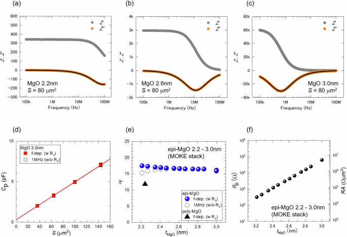
a–c f dependence of Z’ (gray circles) and Z” (orange circles) for devices with tMgO = 2.2, 2.6, and 3.0 nm. The black lines indicate the fitting curves obtained using Eq. (2). d S dependence of Cp for the epitaxial MgO tunnel barrier with tMgO = 3.0 nm. The red closed squares represent Cp values obtained from the frequency dependence of Z” considering Rs. The open squares represent Cp values obtained from the impedance at 1 MHz, ignoring Rs. e tMgO dependence of εr for epitaxial MgO tunnel barriers with 2.2 ≤ tMgO ≤ 3.0 nm obtained by fitting the f dependence of Z” (blue closed circles) and obtained from the impedance at 1 MHz (open circles). εr of the polycrystalline MgO tunnel barrier with tMgO = 2.2 nm is also represented by the black triangle. f tMgO dependence of Rp (left axis) and RA (right axis) for epitaxial MgO tunnel barriers with 2.2 ≤ tMgO ≤ 3.0 nm.
We also investigated εr for devices with a polycrystalline MgO tunnel barrier composed of Ta (5 nm)/Ru (10 nm)/Ta (5 nm)/Fe80B20 (1.6 nm)/MgO (2.2 nm)/cap (MOKE device) and obtained εr = 11.8 for the polycrystalline MgO tunnel barrier with tMgO = 2.2 nm. The εr of the polycrystalline MgO tunnel barrier is indicated by the black triangle in Fig. 2e. See Supplementary Information S3 for further details. The value of εr = 11.8 is slightly larger than that of the MgO bulk (~10.0), but it is smaller than that of the epitaxial MgO tunnel barriers (15.9–17.5), indicating the importance of the epitaxial stack in obtaining large εr values.
Evaluation of epitaxial strain of MgO tunnel barriers
Here, we focus on the effect of the epitaxial strain of the MgO tunnel barrier as the origin of the variation in εr, as shown in Figs. 1f and 2e. The strain-induced increase in εr in rocksalt oxides has previously been investigated both theoretically22,23,24 and experimentally25,26. When the c-axis is stretched due to compressive strain, the electron orbital overlap between cations and anions in the c-direction decreases. Softening of the optical phonon mode then occurs, resulting in an increase in εr. Such compressive strain can occur in the epitaxial stack due to lattice mismatch, as the (sqrt{2}a) of the Cr buffer layer (4.08 Å) is much smaller than the a of MgO (4.21 Å). Thus, we investigated the changes in the lattice constant, a, of the MgO tunnel barrier of the samples with respect to tMgO. Figure 3a shows the in-plane XRD patterns of samples with tMgO = 4.0, 6.0, 8.0, and 10.0 nm. The dashed black line and blue arrows indicate the MgO (002) peak positions of the MgO substrate and MgO tunnel barriers, respectively. The (002) peak of the MgO tunnel barriers exists at a higher angle than that of the MgO substrate, indicating a smaller a. With increasing tMgO, the peak position shifts to a lower angle. Figure 3b shows the tMgO dependence of a of the MgO tunnel barriers. The a value of the 4-nm-thick MgO is 4.15 Å, which is between the (sqrt{2}a) values of Cr and bulk MgO. This indicates that the MgO tunnel barrier is tetragonally compressed because of restraint from the underlying layers, such as the Cr buffer layer. With increasing tMgO, the a of the MgO tunnel barrier increases and approaches that of bulk MgO. This trend may reflect the lattice relaxation of the MgO tunnel barrier with the introduction of misfit dislocations. The detection depth of the in-plane XRD measurements is greater than tMgO. Therefore, the obtained a value represents the mean value throughout the MgO tunnel barrier. We deduce that the a of the MgO tunnel barrier changes gradually along the film thickness direction with the introduction of misfit dislocations, resulting in a change in the mean a value with tMgO. Figure 3c shows a plot of the εr of the MgO tunnel barriers against the mean a. The lattice strain, Δa, is also shown on the upper axis. We find that as a decreases, corresponding to larger compressive strain, εr increases. This result demonstrates the increase in εr of the MgO tunnel barrier due to epitaxial strain. Based on previous reports22,23,25, as compressive strain is applied to rocksalt oxide, softening of the optical phonon mode occurs, and the phonon frequency decreases. When a critical strain is applied and the phonon frequency becomes imaginary, the inversion symmetry along the c-axis is removed, and the rocksalt oxide becomes ferroelectric. The εr value increases with increasing compressive strain and diverges at the critical strain. The critical strain for MgO is estimated to be −7.4%22, which is greater than the strain of the 4.0-nm-thick MgO tunnel barrier in this study (−1.5%). Therefore, Fig. 3c may represent a nonlinear increase in εr toward the critical strain. On the other hand, as previously discussed, the increase in εr was smaller for the MgO tunnel barrier in the polycrystalline stack. In the polycrystalline stack, because the MgO (001) plane preferentially grows on the amorphous Fe80B20 layer, the MgO tunnel barrier may receive less lattice strain from the underlying layer. The smaller εr value of the polycrystalline MgO tunnel barrier ensures the dominant contribution of the epitaxial strain in enhancing the εr of the epitaxial MgO tunnel barriers.
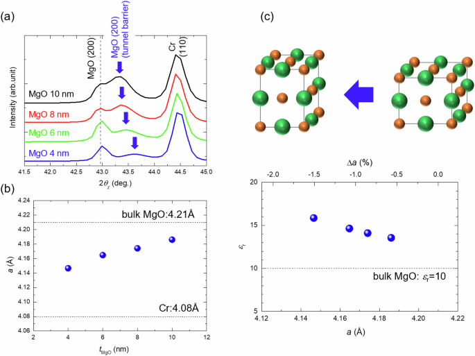
a In-plane 2θχ/ϕ XRD patterns of samples with tMgO = 4.0, 6.0, 8.0, and 10.0 nm along the MgO (200) plane. b MgO thickness dependence of the lattice parameter a of the MgO tunnel barrier. c Variation in εr of the MgO tunnel barrier with respect to the lattice parameter a (lower axis) and lattice strain Δa (upper axis).
Influence of the variation in the dielectric constant on the VCMA effect
Finally, we examined the effect of the εr variation on the VCMA coefficient. The VCMA effect was investigated by measuring the perpendicular magnetization curve using MOKE while a bias electric field was applied. We designed the epitaxial stacks such that the ferromagnetic layer exhibited moderate in-plane magnetic anisotropy to investigate the change in the magnetic anisotropy induced by a bias electric field from the perpendicular magnetization curve. Figure 4a, b show the perpendicular magnetization curves under a bias electric field for devices with tMgO = 4.0 and 10.0 nm, respectively. For both devices, a clear increase in the saturation magnetic field, Hk, was observed upon the application of a positive electric field (orange and red curves), whereas a decrease in Hk was observed upon the application of a negative electric field (light blue and blue curves). Based on the perpendicular magnetization curves measured by MOKE and the saturation magnetization values measured by VSM, we evaluated the effective magnetic anisotropy energy, Keff, using the same procedure as that in our previous reports13,27,28. Figure 4c shows the bias electric field dependence of KefftFM for the devices with tMgO = 4.0 and 10.0 nm, where tFM denotes the total thickness of the Fe/Ir/Co ferromagnetic layers, i.e., 1.06 nm. All samples exhibited a linear magnetic anisotropy change under the bias electric field. The slope represents the VCMA coefficient. The evaluated VCMA coefficients were −255 and −212 fJ/Vm for the devices with tMgO = 4.0 and 10.0 nm, respectively. Figure 4d shows the tMgO dependence of the VCMA coefficient for the devices with 4.0 ≤ tMgO ≤ 10.0 nm. The VCMA coefficient tended to increase with decreasing tMgO. This trend is the same as that for the εr variation shown in Fig. 1f. In other words, we confirmed the increase in the VCMA coefficient through epitaxial strain-induced εr enhancement. Figure 4e shows the VCMA coefficient plotted versus εr for devices with tMgO = 4.0, 6.0, 8.0, and 10.0 nm. The VCMA coefficient increases almost proportionally with increasing εr; comparing devices with tMgO = 4.0 and 10.0 nm, it is observed that the VCMA coefficient increases by 1.2 times (−216.5 to −256.0 fJ/Vm), and εr increases by 1.2 times (13.6 to 15.9). Figure 4f shows the tMgO dependence of the VCMA coefficient for the devices with 2.2 ≤ tMgO ≤ 3.0 nm. An increasing trend in the VCMA coefficient with decreasing tMgO is observed for devices with tMgO ≥ 2.4 nm, taking the relatively large measurement dispersion of the VCMA coefficient into account (blue closed circles). On the other hand, for tMgO < 2.4 nm, VCMA deviates from the increasing trend and gradually decreases with decreasing tMgO (blue open circles). This deviation may be due to the influence of the voltage drop at the electrode as the resistance of the MgO tunnel barrier approaches the resistance of the electrode. From the capacitance measurements, we estimated Rp of the 2.2-nm-thick MgO tunnel barrier to be approximately 300 Ω (Fig. 2f), whereas the resistance of the electrode (Rs) was 24 Ω. The resistance of the probe also contributes to the voltage drop. Considering these resistance values, a voltage drop of approximately 10%, and thus a decrease of approximately 10% in the VCMA coefficient, is expected to occur for devices with tMgO = 2.2 nm. Note that the relatively large device size of the MOKE devices (80 μm2) reduced Rp, leading to an obvious voltage drop at the electrode for the device with tMgO = 2.2 nm. Because the typical MTJ size is several orders of magnitude smaller, such a voltage-drop effect is not visible until the MgO film becomes much thinner.
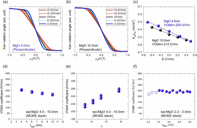
a, b Perpendicular magnetization curves under an electric field for devices with tMgO = 4.0 and 10.0 nm measured by MOKE. c Electric field dependence of KefftFM for devices with tMgO = 4.0 and 10.0 nm. d, e tMgO and εr dependence of the VCMA coefficient for devices with 4.0 ≤ tMgO ≤ 10.0 nm. f tMgO dependence of the VCMA coefficient for devices with 2.2 ≤ tMgO ≤ 3.0 nm.
In the thick MgO region (4.0 ≤ tMgO ≤ 10.0 nm), εr, lattice strain, and VCMA coefficient show consistent tends, confirming the reliable evaluation of εr. On the other hand, in the thin MgO region, since the thickness-dependent trend of the VCMA coefficient deviates from that of εr, the reliability of the εr evaluations is unclear. Therefore, we investigated the VCMA effect and εr of MTJ stacks with smaller device sizes and compared their thickness-dependent trends. We prepared a sample of an epitaxial MTJ stack consisting of MgO (001) substrate/Cr (50 nm)/Fe (0.5 nm)/Ir (0.06 nm)/Co (0.1 nm)/MgO (tMgO nm)/Fe (10 nm)/cap with three different MgO thicknesses (tMgO = 2.0, 2.5, and 3.0 nm), as shown in Fig. 5a. In this stack, the top 10 nm-thick Fe acted as a reference layer with an in-plane magnetic easy axis, resulting in an orthogonal magnetization configuration with the bottom Fe/Ir/Co perpendicular free layers under zero magnetic field. The application of an in-plane magnetic field tilted the magnetization of the Fe/Ir/Co free layers to the in-plane direction, which can be observed through the TMR effect. By investigating the bias electric field dependence of the TMR effect, we investigated the VCMA effect using the same procedure as that in our previous report29. The measurement procedures are described in detail in Supplementary Information S4. Figure 5b shows the tMgO dependence of the VCMA coefficient for the epitaxial MTJ devices with tMgO = 2.0, 2.5, and 3.0 nm. At each tMgO, the VCMA coefficients of more than 10 devices were measured. The error bars account for the variation in the VCMA coefficient for each device as well as the variation in tMgO within the sample (3%). Note that the nonlinear uncertainty of the VCMA coefficient caused by the variation in the free layer thickness is not included in the error bars. The VCMA coefficient remains almost constant or increases slightly with decreasing tMgO from 3.0 to 2.0 nm, taking the error bars into consideration. By measuring MTJs with a small device size, we confirmed that the VCMA coefficient does not decrease even when tMgO is reduced to 2.0 nm. Figure 5c shows the tMgO dependence of εr for MTJ devices with tMgO = 2.0, 2.5, and 3.0 nm. The error bars account for the variation in Cp for each device as well as the variation in tMgO within the sample (3%). For devices with tMgO = 2.0 nm, the uncertainty of the fitting f dependence of Z” (1%), as discussed in Supplementary Information S2, is also considered. We obtained a thickness-dependent trend consistent with the VCMA coefficient; εr also remains almost constant or increases slightly with decreasing tMgO, taking the error bars into consideration. Note that the rate of increase in εr in the range of 4.0 ≤ tMgO ≤ 10.0 nm is as small as 3% per nm. While it is difficult to determine whether εr increases at this rate in the range of 2.0 ≤ tMgO ≤ 3.0 nm, it is confirmed that the εr is at least maintained at tMgO = 2.0 nm. We also investigated the VCMA effect and εr of MTJ devices with polycrystalline MgO tunnel barriers for the same tMgO range (tMgO = 2.0, 2.5, and 3.0 nm) and confirmed that the changes in the VCMA coefficient and εr in this range are within the error bars (see Supplementary Information S5). Finally, from the perspective of practical application, we would like to comment on the εr of devices with lower tMgO and smaller device sizes. With respect to lower tMgO, if we consider the origin of the variation in the lattice strain shown in Fig. 3b as lattice relaxation accompanied by the introduction of misfit dislocations, the lattice strain becomes unchanged below a certain critical thickness. According to the transmission electron microscopy (TEM) image of the epitaxial MgO tunnel barrier fabricated by electron-beam evaporation technique in a previous report30, misfit dislocations are rarely observed in the 2.3 nm-thick MgO layer, except at the interface. This suggests that the lattice strain and thus the εr of the epitaxial MgO tunnel barrier will not increase significantly below this thickness. We assume that even when the tMgO decreases further, such a lattice strain-induced increase in εr is maintained, and εr converges to approximately 17−18. On the other hand, independent of the lattice strain, if an interfacial layer with a lower εr is formed, the εr of the dielectric film decreases with decreasing film thickness. In this study, such a decrease in εr was not clearly observed at tMgO = 2.0 nm, indicating the absence of an apparent interfacial layer at the high-quality interface of epitaxial MgO-MTJs. Another theory indicates that even in the absence of an interfacial layer, εr of the dielectric film may decrease with thickness due to the intrinsic size effect31,32. However, the size effect is remarkable when the bulk εr of the dielectric film is very large (e.g., εr > 100). Our estimation based on ref. 32 indicated that a decrease in εr of only ~8% will occur for a 1.0-nm-thick dielectric film when the bulk εr is 10 (see Supplementary Information S6). Since the epitaxial MgO tunnel barrier has a relatively large εr of ~18, we assume that a 10−20% decrease in εr may occur for 1.0-nm-thick MgO. With regard to device size, since lattice strain is introduced during the epitaxial growth of the MgO tunnel barrier, the lattice strain is not relieved during the subsequent microfabrication process. While there may be other factors that affect εr in addition to the lattice strain, generally, εr is considered to be less sensitive to device size. In addition, past size-dependent VCMA coefficient measurements suggested that the VCMA coefficient does not decrease with decreasing device size down to 50 nmϕ 33,34. Therefore, we believe that εr does not decrease with decreasing device size; however, further verification is required.
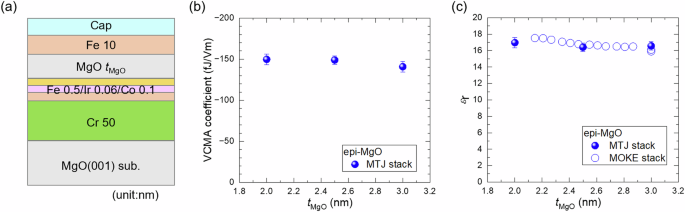
a Schematics of the epitaxial MTJ stack used in the present study. b tMgO dependence of the VCMA coefficient for epitaxial MgO MTJ devices with tMgO = 2.0, 2.5, and 3.0 nm. c tMgO dependence of εr for epitaxial MgO MTJ devices with tMgO = 2.0, 2.5, and 3.0 nm (blue closed circles). The εr of epitaxial MgO MOKE devices are also shown by open circles.
In this study, we demonstrated an increase in the εr of MgO tunnel barriers owing to lattice strain and an associated increase in the VCMA coefficient in epitaxial stacks, which is smaller in polycrystalline stacks. To date, large VCMA coefficients exceeding −300 fJ/Vm have been observed only in epitaxial MTJs19,35,36,37, whereas VCMA coefficients of up to approximately −100 fJ/Vm have been observed in polycrystalline stacks38,39,40,41,42. This difference mainly be due to the difference in the ferromagnetic layers. In epitaxial MTJs, a large VCMA coefficient has been realized through precise subnanometer-scale control of the thickness of ferromagnetic and heavy metal layers. It has also been reported that the presence of B, which is commonly used in polycrystalline MTJs, suppresses the increase in the VCMA coefficient caused by heavy metal doping38. On the other hand, this study clarified the nonnegligible influence of the differences in the εr of MgO tunnel barriers on the VCMA coefficient. Our study provides a new perspective that the strain-induced εr enhancement of the MgO tunnel barrier is another effective approach to increase the VCMA coefficient, in addition to the development of ferromagnetic materials. Strain engineering makes simple rocksalt tunnel barriers more attractive.
Conclusions
In this study, we systematically investigated the dielectric constant (εr), lattice parameter (a), and VCMA coefficient of MgO tunnel barriers in epitaxial stacks. We observed a trend of increasing εr of the MgO tunnel barrier with decreasing MgO thickness. We obtained much larger εr values of approximately 17 for epitaxial MgO tunnel barriers with 2.0 ≤ tMgO ≤ 3.0 nm than for bulk MgO (~10). We also observed an increase in the VCMA coefficient associated with the increase in εr with decreasing MgO thickness. In-plane XRD measurements revealed that the mean a value decreased with decreasing MgO thickness, indicating the presence of tetragonal compression of the MgO tunnel barrier due to epitaxial strain. We concluded that tetragonal compression enhanced the εr of the MgO tunnel barrier and thus the VCMA coefficient in the epitaxial stacks. The strain-induced increase in εr was maintained at tMgO = 2.0 nm. Strain engineering is an effective approach to improve the characteristics of simple rocksalt tunnel barriers.


Responses