Giant memory window performance and low power consumption of hexagonal boron nitride monolayer atomristor

Introduction
Two-dimensional (2D) materials have emerged at the forefront of material science research, promising advancements in nanoelectronics and nanotechnologies1,2,3,4,5,6,7,8,9,10,11,12,13. These 2D materials, including graphene, transition metal dichalcogenides (TMDs), and hexagonal boron nitride (h-BN), exhibit outstanding electrical, mechanical, and optical properties not readily found in their three-dimensional (3D) bulk counterparts14,15,16,17,18,19,20. Their ultrathin nature enables the fabrication of atomic-scale devices and circuits for high-density and low-power electronic applications21,22,23,24,25,26,27. However, unlike 3D bulk materials, 2D materials are typically grown on wafer-scale substrates through chemical vapor deposition (CVD), molecular beam deposition (MBE), or metal-organic chemical vapor deposition (MOCVD) and subsequently transferred to target substrates through dry or wet transfer methods with the aid of numerous polymer support layers, such as polydimethylsiloxane (PDMS), polymethyl methacrylate (PMMA), or polystyrene (PS)28,29,30,31,32,33,34,35,36,37. While these 2D materials possess favorable material properties, such as a highly crystalline lattice and clean surface, various morphological defects can arise during their growth or transfer processes to fabricate 2D devices and circuits. The localized or interfacial defects, such as wrinkles and contaminant particles, created during the transfer processes can significantly degrade the performance of these devices and circuits38,39,40,41,42,43. In particular, in the vertical metal-insulator-metal (MIM) memristor structures, cracks and wrinkles can lead to significant yield degradation, while contaminant particles can result in unclean interfaces and variability44,45. Therefore, it is crucial to select the transfer support layer based on how intact it can cleanly transfer ultrathin 2D materials.
The memory resistive switching effects have been demonstrated by atomic-scale memristor (atomristor) metal-insulator-metal (MIM) structures of 2D TMD and h-BN monolayers46,47,48,49,50,51,52. The memory switching mechanism of the 2D atomristors using gold (Au) electrodes has suggested that the resistive switching effects are attributed to the adsorption/desorption of metal atoms into the intrinsic vacancies of the monolayers53,54. Furthermore, recent research on atomristors using silver (Ag) electrodes has demonstrated that the transition between volatile and nonvolatile switching is attributed to the thickness and stiffness of the conductive bridge formed at the polymeric-residue-contaminated interface between the monolayer and electrode55. However, ironically, most atomristors have faced significant endurance and yield issues due to the extremely thin nature of the monolayers56,57. Therefore, it is necessary to find a new transfer support layer that can minimize the wrinkles and contaminant particles in the metal-insulator-metal structures created during the transfer processes of these ultrathin monolayers.
Recently, Mondal et al. reported that a polypropylene carbonate (PPC) support layer significantly reduce wrinkles and residues than the PMMA support layer during the wet transfer process of the molybdenum disulfide (MoS2) monolayer58. This prior works aids in understanding that the PPC support layer was able to acquire fewer wrinkles during the transfer and annealing processes due to its higher elastic modulus and lower thermal expansion coefficient than the PMMA support layer and to minimize residues due to its superior solubility in solvent stripper58,59,60,61,62.
This work investigates the giant memory window performance and low power consumption of the nanoscale nonvolatile atomristor structures using the h-BN active monolayer and Ag metal electrodes through a PPC-assisted wet transfer method. In particular, we focused on the minimization of cracks, wrinkles, and residues that have the most significant influence on the endurance and yield of the atomristors through polymer support layer and solvent stripper replacements. The endurance and yield of the h-BN atomristor showed a noticeable improvement while maintaining the highest memory window and the smallest leakage current among other 2D atomristors. This marks the first successful demonstration of a PPC-assisted wet transfer method for transferring the ultrathin and large-area h-BN monolayer. We have demonstrated the enhancements in switching and reliability performances of the vertical atomristor structures for practical high-performance and energy-efficient neuromorphic computing systems.
Results
Device characterization and fabrication of hexagonal boron nitride atomristor
Figure 1a and b provide the schematic illustrations of the h-BN atomristor using symmetric Ag metal electrodes. The h-BN atomristor was fabricated by sandwiching the h-BN monolayer between the top and bottom Ag electrodes to stimulate the formation and breakage of conductive bridges at either the top or bottom electrodes (Supplementary Fig. 1)54,55. Figure 1c presents the optical microscopy (OM) image of the h-BN atomristor. The junction area of the MIM structure is measured to be around 0.40 × 0.40 μm2. Figure 1d shows the atomic force microscopy (AFM) images of the h-BN atomristor on the diamond substrate. The thicknesses of the top and bottom Ag metal electrodes are measured to be around 90 nm and 50 nm, while the thickness of the h-BN monolayer on the clean SiO2/Si substrate is estimated to be about 0.51 nm due to the van der Waals gap between the monolayer and substrate (Supplementary Fig. 2)51,55. Figure 1e shows the atomic-resolution transmission electron microscopy (TEM) image of the h-BN monolayer on the SiO2/Si substrate. The lattice constant of the honeycomb structure is around 2.5 Å, in agreement with the theory19. Figure 1f shows the Raman spectra of the h-BN monolayer with a characteristic peak around 1360 cm−1 consistent with the material structure63.

a, b Schematic illustrations of the h-BN atomristor using the Ag electrodes. c OM image of the h-BN atomristor on the polycrystalline diamond substrate. The junction area of the atomristor structure is measured to be around 0.40 × 0.40 µm2. d Topological AFM image of the h-BN atomristor on the diamond substrate. The thicknesses of top and bottom Ag metal electrodes are measured to be around 90 nm and 50 nm. e Atomic-resolution TEM image of the h-BN monolayer on the on the SiO2/Si substrate. Reproduced with permission from GrollTex, Inc. f Raman spectra of the h-BN monolayer on the on the SiO2/Si substrate consistent with its Raman mode.
Hexagonal boron nitride monolayer wet transfer using PPC support layer
Figure 2a and b show the OM images of the bottom Ag electrodes on the diamond substrates after wet transfer of the h-BN monolayer using PPC and PMMA support layers (Supplementary Fig. 3). Unlike the PMMA-coated substrate, there was no need to scratch the sidewalls of the PPC-coated substrate with a diamond scriber due to the high viscosity of the PPC support layer (Supplementary Fig. 4). As a result, the sidewalls of the transferred PPC/h-BN stacking layer were significantly cleaner than those of the transferred PMMA/h-BN stacking layer on the target substrate (Supplementary Fig. 5). It was found that the PPC/h-BN stacking layer on the diamond substrate has no wrinkles, while the PMMA/h-BN stacking layer has tens of micrometers of wrinkles in a region of interest. This suggests that the stiffness of the PPC support layer is much greater than that of the PMMA support layer because elastic modulus of the PPC support layer (~993 MPa) is higher than that of the PMMA support layer (~8 MPa)34,59,60,64. Furthermore, the PPC/h-BN and PMMA/h-BN stacking layers were annealed to remove water droplets after they were transferred from deionized (DI) water to the diamond substrates. The water droplets were removed without the contraction of the PPC/h-BN stacking layer, while the PMMA/h-BN stacking layer contracted and formed micrometers of wrinkles. This is because the thermal expansion coefficient of the PPC support layer is close to that of the h-BN monolayer and is much lower than that of the PMMA support layer34,58,65. However, it was challenging to visually differentiate the transferred h-BN monolayer from the diamond substrate after dissolving the polymer support layers.

a, b OM images of bottom Ag metal electrodes on the substrate after transferring h-BN monolayer using PPC and PMMA support layers. c–e High-resolution OM and topological AFM images of h-BN monolayer on SiO2/Si substrate before and after removing the PPC support layer. The area coverages of the transferred h-BN monolayer and PPC residues are estimated to be around 96% and 0.55%. f–h High-resolution OM and topological AFM images of h-BN monolayer on the same substrate before and after removing the PMMA support layer. The area coverages of the transferred h-BN monolayer and PMMA residues are estimated to be about 90% and 2.1%.
To further investigate this, we transferred the PPC/h-BN and PMMA/h-BN stacking layers onto bare SiO2/Si substrates to characterize the physical and chemical properties of each polymer support layer. The h-BN monolayer transfer is more likely to create many cracks than the h-BN multilayer transfer during the dissolution of the polymer support layers, so we chose acetone as solvent stripper rather than anisole (~1.3 kPa) and remover PG (~0.039–0.043 kPa) due to its higher vapor pressure of 25 kPa at room temperature (Supplementary Fig. 6). Figure 2c and d show the OM images of the transferred h-BN monolayer on the bare SiO2/Si substrate before and after dissolving the PPC support layer. Figure 2e presents the topological AFM images of the remaining PPC residues on the transferred h-BN monolayer on the SiO2/Si substrate. Figure 2f and g shows the OM images of the transferred h-BN monolayer on the same substrate before and after removing the PMMA support layer. Figure 2h represents the topological images of the remaining PMMA residues on the transferred h-BN monolayer on the same substrate. The area coverage of the PPC-assisted transferred h-BN monolayer is measured to be about 96%, while that of the PMMA-assist transferred monolayer is estimated to be around 90% (Supplementary Fig. 7). It is noticeable that the cracked and wrinkled areas of the PPC-assisted transferred h-BN surface are much smaller than those of the PMMA-assisted transferred surface. Furthermore, the area coverages of the PPC and PMMA residues are extracted to be around 0.55% and 2.1% (Supplementary Fig. 8). It has been found that both the number and size of the PPC residues are significantly less than those of the PMMA residues. This is because the PPC support layer has better solubility in acetone than the PMMA support layer, thereby minimizing polymer residues that could degrade atomristor performance58,61,62.
Memory window performance of hexagonal boron nitride atomristor using silver metal electrodes
Figure 3a shows the static current-voltage (I–V) characteristics of the 0.40 × 0.40 μm2 h-BN atomristor using symmetric Ag electrodes at 1 mA current compliance. The h-BN atomristor exhibits nonvolatile bipolar resistive switching behaviors with a giant memory window of more than 109, while the operating voltage and leakage current is measured to be less than 0.16 V and 5.7 pA. Figure 3b provides the statistical SET voltage (VSET) and RESET voltage (VRESET) distributions of the 43 atomristors at the same current compliance and atomristor area. Taking advantage of the PPC support layer, we fabricated 56 atomristors on the same substrate and improved the yield rate to 77% (= 43/56 × 100%) (Supplementary Fig. 9). The mean (µ) values of VSET and VRESET are estimated to be about 0.96 V and −0.25 V, and the standard deviation (σ) values of these switching voltages are extracted to be around 0.44 V and 0.13 V with the coefficients of variation (CV) of 46% and 52%. Figure 3c presents the statistical high-resistance-state resistance (RHRS) and low-resistance-state resistance (RLRS) distributions of the same atomristors at 1 mA current compliance. The µ and σ values of RHRS are measured to be about 440 GΩ and 890 GΩ with a CV of 200%, while these values of RLRS are calculated to be around 230 Ω and 170 Ω with a CV of 71%.
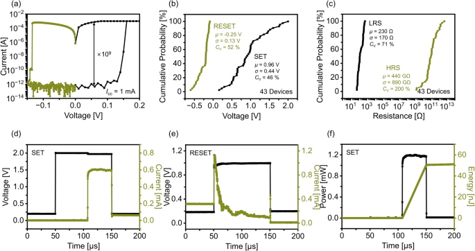
a Static I–V characteristics of the 0.40 × 0.40 µm2 h-BN atomristor. b, c Statistical VSET/VRESET and RHRS/RLRS distributions of 43 h-BN atomristors. The µ and σ values of VSET are measured to be 0.96 V and 0.44 V, while these values for VRESET are estimated to be –0.25 V and 0.13 V. The µ values of RHRS and RLRS are extracted to be 440 GΩ and 230 Ω, but the σ values of those state resistances are measured to be 890 GΩ and 170 Ω. d, e Microsecond VIN and IOUT pulse waveform characteristics of the h-BN atomristor during the SET and RESET processes. The VSET and VRESET pulse amplitudes were set to approximately 2.0 V and −1.0 V with the same pulse width of 100 µs. The VREAD pulse amplitude was set to around 0.2 V before and after the VSET and VRESET pulses. The switching speeds of the initial SET and RESET processes are measured to be about 57 µs and 1.7 µs, respectively. f Microsecond consumed power and energy characteristics of the h-BN atomristor during the initial SET process. The consumed energies are calculated to be 50 nJ for the SET process.
Figure 3d and e present the microsecond input voltage (VIN) and output current (IOUT) pulse waveform characteristics of the h-BN atomristor for both SET and RESET processes. The VSET and VRESET pulse amplitudes were set to approximately 2.0 V and –1.0 V with the same pulse width of 100 µs. The pulse amplitude of the READ voltage (VREAD) was set to around 0.2 V before and after the VSET and VRESET voltage pulses. The switching speeds are measured to be about 57 µs for the SET process and 1.7 µs for the RESET process, at which the Ag metal atom begins to move after the voltage pulse is applied66,67,68. Interestingly, the switching speed of the second SET process (~14 µs) is 4 times faster than that of the first SET process (~57 µs) because the remaining Ag metal atoms were significantly utilized to form the conductive bridge between the surfaces even at lower energies (Supplementary Fig. 10)55. Furthermore, it clearly showed the transition for each resistance state through the IOUT pulse measurements during subsequent READ processes. This indicates that a transition from high-resistance-state (HRS) to low-resistance-state (LRS) requires a greater pulse amplitude and a broader pulse width of input voltage than a transition from LRS to HRS.
Figure 3f shows the microsecond consumed power and energy characteristics of the h-BN atomristor for the initial SET process. The VIN pulse waveform was multiplied by the IOUT pulse waveform to extract the power consumption during each switching process, and the energy consumption was calculated by integrating this power consumption over the switching time50. The energy consumption was measured at 50 nJ for the initial SET process and 23 nJ for the subsequent RESET process (Supplementary Fig. 11). This demonstrated that the energy barrier for the initial SET process is more significant than that for the subsequent RESET process, attributed to a mechanism where the Ag metal atoms have a strong tendency to aggregate into the clustered Ag metal electrode55,69. The total energy consumption for the second SET process increased from 60 nJ to 81 nJ through multiple reaction steps of conductive bridge formation (Supplementary Fig. 12)55. The remaining Ag metal atoms are likely to reduce the energy barrier to form the conductive bridge, so the conductive bridge for the second SET process was formed much thicker and faster than that for the initial SET process, even under the same pulse conditions55.
Memory endurance performance of hexagonal boron nitride atomristor using silver metal electrodes
Figure 4a shows the ramped-voltage-stress (RVS) endurance performance of the h-BN atomristor at 1 mA current compliance. The RVS endurance is measured to be 139 switching cycles. The statistical VSET and VRESET distributions of the h-BN atomristor were measured at 139 switching cycles through the RVS endurance measurements. The µ and σ values of VSET are estimated to be about 3.3 V and 1.7 V with a CV of 52%, but those values of VRESET are extracted to be about −1.7 V and 1.4 V with a CV of 83% (Supplementary Fig. 13a). The statistical RHRS and RLRS distributions of the h-BN atomristor were also measured at the same switching cycles through the same measurements. The µ values of RHRS and RLRS are calculated to be around 550 GΩ and 220 Ω, and the σ values of each state resistance are extracted to be about 1.2 TΩ and 180 Ω with a CV of 220% and 80% (Supplementary Fig. 13b). It was found that the statistical distributions of resistance for each state are almost the same between device-to-device and cycle-to-cycle variability results because the maximum current was restricted by the current compliance setting of the measurement equipment46,47,48. Figure 4b presents the memory retention characteristics of the h-BN atomristor at 1 mA current compliance. The memory retention was measured to be more than 105 s (~28 h) with a memory window of 108. This demonstrates that the h-BN atomristor using the PPC support layer showed improved endurance and retention performances compared to that using the PMMA support layer, even under the same fabrication and measurement conditions because the number and size of the PPC residues are significantly smaller than those of the PMMA residues after dissolving with acetone. This reduced residual effect causes the decreased interfacial distance between the h-BN and Ag surfaces and forms more stable conductive bridges between the surfaces51,55. Furthermore, we conducted the pulsed-voltage-stress (PVS) endurance measurements of the h-BN atomristor using repeated VSET and VRESET pulses. The PVS endurance was measured to be more than 10,000 switching cycles, but the memory window was reduced to about 104 due to the instrumental limitation of the measurement equipment (Fig. 4c). The VSET and VRESET pulse amplitudes were set to 1.0 V and –0.4 V with the same pulse width and period of 30 ms and 50 ms. This indicates that reliable PVS endurance measurements were achievable even in the Ag/h-BN/Ag atomristor structures because the reduced interfacial distance between the h-BN and Ag surfaces decreased the energy barrier for the dissociation of Ag atoms (Fig. 4d)55. However, further characterization is needed to investigate the combined mechanisms of defect and interface engineering in the atomristor structures.
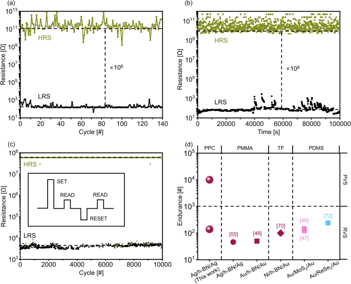
a RVS memory endurance performance of the h-BN atomristor. The RVS endurance is measured to be 139 switching cycles with a memory window of 108. b RVS memory retention characteristics of the h-BN atomristor. The memory retention time is estimated to be more than 105 s (~28 h). The dashed lines are a visual guide. c PVS endurance performance of the h-BN atomristor. The VSET and VRESET pulse amplitudes are set to 1.0 V and −0.4 V with the VREAD pulse amplitude of 0.3 V. Each pulse width and period are set to 30 ms and 50 ms. The PVS endurance is measured to be more than 10,000 switching cycles. d RVS and PVS memory endurance characteristics of the atomristors using various monolayers, electrodes, and transfer support layers.
Figure-of-merit comparison of memory window and endurance performances of two-dimensional monolayer atomristors
Figure 5 represents the figure-of-merit comparisons of nonvolatile memory switching performances of the h-BN atomristor using symmetric Ag electrodes with other 2D monolayer atomristors. Our best h-BN atomristor shows the highest memory window of 4 × 10⁹ and relatively small switching voltages of less than 0.16 V, attributed to the high band gap of the h-BN monolayer (~6.0 eV) and low energetics of the Ag metal electrodes. The µ values of device-to-device variability results are also represented by the memory window of 2 × 10⁹, along with the switching voltages and power consumption for SET and RESET processes. In addition, the h-BN atomristor using the PPC-assisted wet transfer method (139 switching cycles) has RVS endurance performance more than 3 times better than that using the PMMA transfer method (46 switching cycles)55. Furthermore, the h-BN atomristor using symmetric Ag electrodes demonstrates significant improvements in switching voltage and leakage current compared to the atomristor using symmetric Au electrodes48,49,51,54,55. This indicates that symmetric Ag electrodes have greater advantages over symmetric Au electrodes in memory devices and applications. On the other hand, the MoS2 atomristor using symmetric Ag electrodes exhibits low switching voltages of less than 1.0 V when subjected to the same compliance current. However, it demonstrates a limited memory window performance of 102, due to the relatively small band gap of the MoS2 monolayer (~1.8 eV)46. This finding suggests that the memory window is influenced by the combination of 2D monolayer and metal electrodes, while the endurance is determined by the stability of conductive bridge formation in the atomristor structures (Table 1). However, further research into asymmetric electrode structures is needed to characterize the detail switching mechanisms in the atomristor structures that use 2D monolayers as the active layers.
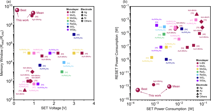
a Memory window versus SET voltage characteristics from the atomristors using various active monolayers and electrodes. This work reports the highest memory window of 4 × 10⁹ and a relatively small VSET of 0.16 V, measured data with the best property from device-to-device variability results. b SET and RESET power consumption characteristics in the atomristors. This work shows the power consumption performances of 2 × 10⁻⁴ W for the SET process and 3 × 10⁻¹⁴ W for the RESET process.
Figure 5b represents a comparison of the figure-of-merit SET and RESET power consumptions of the 2D atomristors, as measured through RVS measurements. Our best h-BN atomristor using symmetric Ag electrodes exhibits the lowest RESET power consumption of around 3 × 10⁻¹⁴ W, attributed to the low VRESET of –0.14 V and high-resistance-state current (IHRS) of around 0.24 pA. Moreover, our best h-BN atomristor shows the lowest SET power consumption of around 2 × 10⁻⁴ W among other 2D atomristors at the same current compliance, attributed to the low VSET of 0.16 V. The μ value of 10−13 W in RESET power consumption also appears lower than that of other 2D atomristors. However, the μ value of 4 × 10⁻³ W in SET power (PSET) consumption shows a slightly larger value than other 2D atomristors, which is still considered competitive given the large memory window. In contrast, the MoS2 atomristor using symmetric Ag electrodes has a RESET power consumption (PRESET) of about 5 × 10⁻⁵ W, which is 9 orders of magnitude higher than the h-BN atomristor using the same electrode because of its relatively smaller bandgap46. Furthermore, the VRESET and IHRS values are measured to be approximately –1.5 V and 10−7 A in the h-BN atomristor using symmetric Au electrodes, with the lowest PRESET of 1.5 × 10⁻⁷ A among the same atomristor structures48.
Discussion
In summary, this work has demonstrated giant memory window performance and low power consumption of symmetric h-BN atomristor structures using Ag metal electrodes via the wrinkle-free and residue-free PPC-assisted wet transfer method. Taking advantage of the superior material properties of the PPC support layer, we fabricated crossbar-shaped Ag/h-BN/Ag atomristor structures and measured their memory-switching behaviors through both RVS and PVS measurements. The h-BN atomristor exhibited the highest memory window of more than 109, the lowest leakage current of about 0.2 pA, and the lowest power consumption of around 10−14 W among other 2D atomristors. The h-BN atomristor also showed a much better memory endurance and retention performance of more than 10,000 cycles and 105 s (~28 h) as the interfacial distance between the h-BN and Ag surfaces became closer to the interfacial equilibrium distance due to the minimization of the polymer residues. Lastly, the yield of the fabricated h-BN atomristors was increased to 77% due to the high elastic modulus and low thermal expansion coefficient of the PPC support layer. This synergistic combination between highly insulating h-BN and electrochemically active Ag electrodes enables improved memristor characteristics at low power for future high-performance and energy-efficient neuromorphic computing components. Device-to-device variation remains a challenge and requires further systematic research studies.
Methods
Material characterization
The optical images of the h-BN atomristor and monolayer were captured by optical microscopy (BX51M-DP22 Metallurgical Microscope, Olympus). The thicknesses of the h-BN atomristor and monolayer were measured by atomic force microscopy (Dimension Icon, Bruker). The area coverage by percentages was obtained by post-processing the optical images using the ImageJ software. Thresholding was applied to identify and mask the regions containing polymeric residue selectively, and the areas of these regions were determined using the software. The Raman peaks of the h-BN monolayer were measured by Raman spectroscopy (inViaTM Confocal Raman Microscope, Renishaw PLC).
Device fabrication
The diamond substrate was rinsed with acetone, methanol, and isopropyl alcohol and dried by a nitrogen spray gun. The 50 nm-thick bottom Ag metal electrode was lithographed by an electron beam (e-beam) lithography system (JBX-8100FS/E, JEOL USA) and deposited on the diamond substrate by an e-beam evaporation system (PRO Line PVD 200, Kurt J. Lesker Company). The h-BN active monolayer was prepared on the 285 nm-thick SiO2/Si substrate and transferred to the diamond substrate through two different PPC-assisted and PMMA-assisted wet transfer methods. The 90 nm-thick top Ag metal electrode was lithographed and deposited on the wet-transferred h-BN active monolayer by the same e-beam lithography and evaporation systems.
Polymer support layer preparation
The PPC pellets (389021-100G, Sigma-Aldrich) were dissolved into the anisole solution (123226-100 ML, Sigma-Aldrich) with a ratio of 15% PPC by weight. The hot plate and magnetic stirrer were used to promote the dissolution of the pellets in the anisole solution over the course of three days.
Material transfer
The CVD grown h-BN monolayer (Grolltex, Inc.) was prepared on the 285 nm-thick SiO2/Si substrate. The h-BN monolayer on the SiO2/Si substrate was rinsed with acetone/methanol/isopropyl-alcohol and dried with a nitrogen spray gun. The PPC support layer was spin-coated on the h-BN grown layer at 4000 rpm for 45 sand baked on the hot plate at 180 °C for 120 s. The PPC/h-BN stacking layer on the SiO2/Si substrate was soaked with the BOE 6:1 until the SiO2 substrate was wet etched with the BOE 6:1. The PPC/h-BN stacking layer was separated from the silicon (Si) substrate and fished to the DI water. The PPC/h-BN stacking layer was rinsed and annealed in DI water on the hot plate at 40 °C. The PPC/h-BN stacking layer was transferred to the diamond substrate and annealed on the hot plate at 100 °C for 120 s to remove the water droplets of DI water. The PPC support layer was dissolved with acetone from the h-BN transferred layer on the diamond substrate.
Device measurement
The RVS measurements were carried out by using a semiconductor device parameter analyzer (B1500A, Keysight Technologies) on a cascade probe station (Summit 11000 AP, FormFactor). The VSET bias was swept from 0.0 V to 2.0 V to 10 V at 1 mA current compliance, while the VRESET was swept from 0.0 V to –0.2 V to –0.8 V without any current compliance. The VREAD bias was swept from 0.0 V to 0.2 V in the same direction as the VSET bias. The PVS endurance measurements were conducted using a semiconductor parameter analyzer (B1500A, Keysight Technologies) on a semiconductor probe station (Summit 11000 AP, FormFactor, Inc.). The block diagram in LabVIEW VI was designed to apply repetitive VSET–VREAD–VRESET–VREAD pulse sequences. LabVIEW from National Instruments was used for the measurement to repetitively apply voltage pulses. The amplitude and width of the VSET pulses were set to 1.0 V and 30 ms, respectively, with a current compliance setting of 100 uA, while the amplitude and width of the VRESET pulses were set to −0.4 V and 30 ms, respectively, with a current compliance setting of 100 mA. Similarly, the amplitude and width of the VREAD pulses were set to 0.3 V and 30 ms, respectively, with a current compliance setting of 100 μA.


Responses