Coupled pyroelectric-photovoltaic effect in 2D ferroelectric α-In2Se3

Introduction
Ferroelectric materials have been changing the paradigm of contemporary science and engineering since Valasek’s first discovery in 19201. Such immense importance stems from their outstanding multifunctionality for non-volatile memory2, field-effect transistors (FET)3,4, actuators5, transducers6, photovoltaics7,8, etc. The pyroelectric effect describes the change in spontaneous polarization with temperature variations, where the net change in dipole moment introduces capacitive current flow that is proportional to the temperature derivative with time dT/dt. This effect is of utmost importance for self-powered infrared thermal-sensing9 and waste heat-energy harvesting10. While the nanoelectronics industry demands the utter miniaturization of the ferroelectrics films, the ultra-low thickness and, hence, low heat capacity entails an extremely small thermal time constant, which is highly beneficial for pyroelectric responsivity11. However, conventional ferroelectrics (CFs) such as perovskite oxides (ABO3) do not often meet such requirements at the nanoscale due to the sharp reduction in spontaneous polarization caused by a strong depolarization field, interfacial defects due to surface reconstruction, electronic screening, etc12,13.
Two-dimensional (2D) materials have been drawing utterly large attention during the past few decades after the first experimental realization of graphene14. Their outstanding and diverse properties such as large surface-to-volume ratio, tunable bandgap15,16,17, ultra-strong light-matter interaction18, excellent thermal and electrical conductivity19,20 etc., drive the constantly growing interest. The recently reported room-temperature stable ferroelectricity in monolayer-thin SnTe21, and in 2D materials possessing dangling bonds and reconstruction-free interfaces such as α-In2Se322 and MoTe223, can address the scaling shortcomings of CFs. In addition, the existing bulk photovoltaic effect in 2D ferroelectrics possesses the potential to overcome the Shockley-Queiseer limit in conventional photovoltaics24,25.
Among 2D ferroelectrics, α-In2Se3 possesses a unique inter-coupled in-plane (IP) and out-of-plane (OOP) polarizations26,27,28,29,30,31, allowing to control the horizontal ferroelectric field via an applied vertical bias and vice versa. In contrast with CFs, which are insulators, In2Se3 is an n-type semiconductor with a direct bandgap of ∼1.4 eV17 that allows its embedding as the channel material of FET and optical sensors26,32. Moreover, recent molecular dynamic simulations revealed a high Curie temperature (Tc) of ∼ 650 K in α-In2Se333, allowing a significantly greater temperature operation range, than Tc = 315 K in CIPS34 or Tc = 340 K in MoTe223. These unique features have found realization in novel optoelectronic memories26,35,36, reconfigurable p-n junctions31,37, and neuromorphic computing38,39,40.
Herein, we demonstrate direct pyroelectric measurement of back-gated FET based on α-In2Se3 under light and dark conditions. The extracted giant pyroelectric coefficient of ∼30.7 mC/m2K and figure of merit of ∼135.9 m2/C reveal a supreme thermal-sensing performance, significantly surpassing CFs41. Under light illumination, the built-in IP polarization and the semiconducting nature of α-In2Se3 introduce the bulk photovoltaic effect, which enables the realization of self-powered and energy-harvesting devices without the need for complex heterostructures fabrication for constructing p-n junctions. Intriguingly, we reveal a coupled pyroelectric-photovoltaic effect where the short-circuit current magnitude linearly follows the temperature modulation while the pyroelectric current follows the temperature derivative. Finally, the back-gate electrode was used to control the IP polarization based on the intercoupled ferroelectricity in In2Se3, allowing to switch the short-circuit current polarity in a non-volatile fashion. The results reveal the extreme temperature-sensitive pyroelectric and photovoltaic effects enabling the detection of temperature and temperature-derivative variations, respectively by the same device. The technology paves the way for integrated monolithic photovoltaic-pyroelectric elements for coupled thermal-sensing and optoelectronic in-memory applications.
Results and discussion
Material characterization
α-In2Se3 flakes were mechanically exfoliated onto a p++-Si substrate covered with 300 nm of SiO2. Source and drain contacts were fabricated using standard electron beam lithography with subsequent metal deposition of 5/50 nm thick Cr/Au metals. Supplementary Figure 1 depicts the AFM topography and Raman spectroscopy analysis. Figure 1a illustrates the experimental setup where the back-gated field effect transistor (FET) was placed onto a programmable heater stage. A broad-band white LED source of spectral range 420–720 nm and intensity of ~332 µW/cm2 was used for device illumination. The generated pyro and photoelectric currents were measured utilizing a semiconductor parameter analyzer (Keysight-B1500A). Figure 1b presents a schematic illustration of the energy band structure and current generation of the pyroelectric-photovoltaic In2Se3 device under light illumination and temperature variations. In particular, temperature variations under dark conditions modify the net dipole moment, which is followed by capacitive current flow to compensate for the change in bound charges. During illumination, the inherent IP ferroelectric field separates the photogenerated electron-hole pairs within the In2Se3 semiconductor channel and creates a short-circuit current. The ferroelectric polarization reduces once the device temperature increases, and the photocurrent monotonically drops. Thus, while the pyroelectric current follows the temperature derivative, the short-circuit current follows the temperature modulation itself. Figure 1c presents the measured polar plot of the normal-incident angular-dependent second-harmonic generation (SHG) before device poling (see Fig. (1d) for the optical microscope image), which indicates the 6-fold inversion-symmetry breaking of the IP polarization in In2Se3. Additional polar plots measured at different locations across the device are depicted in the Supplementary Figure 2. The lobes in Fig. 1c and in the Supplementary Figures 2b–d possess slight asymmetry along different axes, which can potentially be attributed to uniaxial strain42. The six-fold angular symmetry of the SHG polar plot and the cross-sectional HRTEM image (Fig. 1d) corresponds to the R3m space group of 3R-In2Se343,44,45. To demonstrate the presence of both out-of-plane (OOP) and in-plane (IP) polarization components, Piezoelectric force microscopy (PFM) measurements were performed and are included in the Supplementary Figures 3 and 4. The images were taken after two square regions of different sizes were scanned by the AFM tip (contact mode) in which +6 V and −6 V were applied to the tip while the sample was grounded. The included amplitude and phase images demonstrate a clear contrast between the different voltage polarities for both IP (Supplementary Figure 3a) and OOP components (Supplementary Figure 3b), in agreement with previous reports16,26,46.

a Schematic representation of the α-In2Se3 based FET device and the pyroelectric-photovoltaic measurement setup. b Schematic band structure representation of the coexisting pyroelectric and photovoltaic effects. c Polar plot of SHG intensity as a function of the excitation laser polarization (s-s polarization). d Cross-sectional HRTEM image of α-In2Se3 showing R3m space group symmetry (scale bar is 5 nm). The inset image presents the device’s optical image. The red point indicates the area where (c) was measured (scale bar is 10 μm).
Direct pyroelectric measurement
Direct pyroelectric measurement under dark conditions was conducted to retrieve the pyroelectric coefficient and figure of merit (Fig. 2a). The top panel shows the temperature modulation throughout the experiment. In particular, the device was repeatedly heated to 40 °C followed by natural cooling down to 30 °C under ambient conditions. The corresponding temperature derivative dT/dt and the pyroelectric current (Ipyro) are shown in the middle and bottom panels, respectively. Evidently, the measured current clearly follows the temperature derivative, confirming the existence of the pyroelectric effect. The device shows stable performance throughout multiple temperature cycles without current degradation. It is important to note that the current does not change its sign during the cooling cycles, which can be attributed to the substantially smaller temperature derivative during cooling. The pyroelectric coefficient p ∼ 30.7 mC/m2K and the figure of merit ({F}_{v}) ∼135.9 m2/C were calculated using the following equations:
where, Ipyro is the pyroelectric current (the difference between the current maximum and the base values), A—the surface area of the device, T—temperature, cp—specific heat capacity (for In2Se3 is 1.5 J K−1cm−3)47, ε0—permittivity of the free space, and εr—relative permittivity (∼17 for In2Se3)48. Table 1 presents the extracted parameters of this work in comparison with several different CFs (PZT, PVDF, LaTiO3)49,50,51 and recently reported 2D materials and nanomembranes (ZnO, β-In2Se3)52. The extracted giant pyroelectric coefficient and the figure of merit of α-In2Se3 significantly surpass previously reported values for CFs and 2D materials.

The data in the stack plot from top to bottom correspond to temperature, temperature derivative, and the measured pyroelectric current.
Coupled pyroelectric-photovoltaic effect and reconfigurable short-circuit current
Figure 3a presents the measured current (black curve) and temperature (red curve) versus time under dark and light (designated with yellow box) conditions. The device was cyclically heated to ∼40 °C and subsequently naturally cooled to ∼30 °C under ambient conditions. It is observed that the photocurrent linearly follows the temperature instead of its derivative with time. In particular, the short-circuit current reduces with temperature rise due to the corresponding decreases in the IP polarization field. Similarly, the subsequent cooling increases the IP electric field, which restores the previous current level. Importantly, the short-circuit current demonstrates substantial temperature sensitivity of ~20 pA/°C within the 30–40 °C measured range. The distinct response under dark and light conditions is further illustrated in Fig. 3b, c by the enlarged sections from Fig. 3a. In particular, while the pyroelectric effect is prominent in dark conditions, manifested by a current modulation of ∼40 pA for the highest temperature change, illumination of the device generates a greater short-circuit current of ∼1 nA. Figure 3d demonstrates a zoom-in image of the region (marked with a semi-transparent rectangular in Fig. 3c) containing the superposition of photovoltaic and pyroelectric effects. The pyroelectric current peak is superimposed on the photocurrent linear modulation and appears when the temperature derivative reaches its maximum. Importantly, the magnitude of the peak does not alter under illumination and coincides with a pyroelectric current in dark conditions comprising about 40 pA. Accordingly, the photo- and pyroelectric effects independently coexist and can be simultaneously probed. By utilizing both effects, the spectral range of the device can be significantly enlarged, covering visible and infrared radiation. In addition, while standard pyroelectric devices can only detect temperature fluctuations, the semiconducting nature of α-In2Se3 enables the detection of both temperature and temperature-derivative without the need to apply a bias potential across the device. This feature presents a novel combination of thermal and photo-sensing by a coupled pyroelectric-photovoltaic effect within the same material. Next, the intercoupled in-plane (IP) and out-of-plane (OOP) ferroelectricity in α-In2Se3 was used to realize self-powered optoelectronic memory operation based on bulk photovoltaic effect. This unique coupling allows the control of the lateral constant electric field, and hence, the linear electrostatic potential drop by an external vertical voltage stimulus and vice versa26. Hence, 30-s voltage pulses of –100 V (blue curve) and +100 V (red curve) were applied to the back-gate electrode to switch the IP polarization direction (Fig. 3e). During the subsequent photocurrent measurements, the source electrode was kept grounded while zero-volt bias voltage was applied to the drain and the gate electrodes (VD = VG = 0). A broadband white light source was used to generate multiple 10-s light pulses to generate the short-circuit current (see “Methods” section for more details). The switching of the IP field results in two opposite current levels, which can be used as “1” and “−1” in memory or logic applications or for weights with opposite signs, which are attractive for neuromorphic-based image processing53. The device shows a stable short-circuit current generation under several cycles of light pulses without current-level degradation. The extracted response time (~0.6 ± 0.3 s) and quantum efficiency (~2.6 ± 0.4%) of the device are included in the SI section for several different wavelengths within the visible range (Supplementary Figures 5 and 6). Generally, an internal electric field is essential for photocarrier separation and subsequent photovoltaic effect. In our previous study, we demonstrated how the modulation of the IP field results in the creation of multibit photocurrent states, where the IP polarization either impede or facilitate photocarriers transport26. In this respect, p-n junctions with inherent built-in electric field are the most common and efficient way to realize photovoltaic operation. There are multiple articles regarding 2D-based p-n junctions (such as WSe2, MoS2, BP) showing decent quantum efficiency reaching 50%54. The reported quantum efficiencies in photovoltaics based on 2D ferroelectric found to be smaller (e.g., 0.4% in strained MoS2, 3% in CIPS, 2.5% graphene/MoS2/graphene), in comparison with conventional p-n junction25,55. Hence, while the obtained values for α-In2Se3 are small in comparison with conventional p-n junctions, they are of the same magnitude as other ferroelectric-based photovoltaic cells.
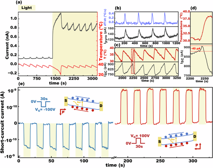
a Current vs. time measurement under dark and light conditions. The yellow transparent box indicates light illumination. The black and red curves correspond to the measured current and temperature, respectively. Zoom in selection from (a) at dark (b) and under illumination (c). b corresponds to the pyroelectric current, which follows the temperature-derivative, whereas (c) corresponds to the short-circuit current under illumination, which monotonically follows the temperature. d Zoom-in to the region (marked with a semi-transparent rectangular in (c)) containing the pyro- and photocurrents superposition. The pyroelectric current peak (∼40 pA) is encapsulated between two red dashed lines. e Short-circuit current after 30-s −100 V (blue) and +100 V (red) gate electrode modulation. The insets schematically demonstrate the change in the surface electrostatic potential slope across the device after the gate voltage withdrawal due to the induced IP polarization.
Temperature dependence pyroelectric-photovoltaic effect and transport characteristics
Figures 4a, b present the temperature-dependent pyroelectric and short-circuit current device characteristics, respectively. The device was gradually heated by 5 °C in two-minute steps from 25 to 60 °C. Figure 4a shows the measurement in dark conditions, where a strong pyroelectric current is generated precisely during the temperature modulation and monotonically decreases with temperature increase. The inset image in Fig. 4a describes a linear correlation between the peak current magnitude and temperature. The base current level at dark caused by thermal generation and subsequent charge separation of electron-hole pairs by the IP polarization reduces with the increase in temperature due to the decrease in the IP field. Under light illumination, the photocurrent decreases from ∼1.5 nA at room temperature to ∼0.5 nA at 65 °C, indicating a substantial temperature sensitivity (Fig. 4b). In both cases, the IP polarization field reduces with increasing temperature, resulting in weaker pyroelectric and photovoltaic effects. Supplementary Figure 7 in the SI section presents a similar measurement that includes both heating and cooling cycles under light and dark conditions. The results show identical current levels prior to the heating and after the cooling cycles, confirming the operation stability. Importantly, the fully restored dark and photocurrent levels upon cooling indicate that the major contribution to the observed current modulations is due to induced changes in the IP field and not due to trapping/de-trapping of fixed charges at the In2Se3 itself or at its interface with the SiO2 support.
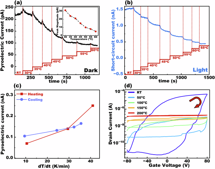
Current vs. time measurements with gradual temperature growth (red lines) in dark (a) and light (b) conditions. Under dark conditions, the pyroelectric current decreases with temperature increase. The inset image shows the linear correlation of the pyroelectric current peak with temperature. Under light, the pyroelectric effect is dominated by the short-circuit current and reduces with temperature growth. c Pyroelectric current vs. temperature modulation rate under heating and cooling. d Temperature dependence of the transfer characteristics under 1 V drain voltage.
The direct pyroelectric measurements performed at ambient conditions (Fig. 2a) possess a slow natural cooling rate, resulting in a minute pyroelectric current. To overcome this, direct pyroelectric characterization was performed in a cryogenic environment using liquid N2 to enhance the cooling power. Starting at a sample temperature of 270 K we were able to generate cooling rates of 10–40 K/min (Supplementary Figure 8). These cooling rates are ∼5–20 times higher than at ambient conditions allowing for measurable pyroelectric current in the opposite direction to the current generated during heating. Figure 4c demonstrates the linear relation between the pyroelectric current and temperature modulation rate for both cooling and heating, which agrees with Eq. (1).
Another device of a similar geometry (see Supplementary Figure 9 for the optical and AFM images) was used to study the temperature dependence of the transfer (ID–VG) (Fig. 4d). The temperature range (from room temperature (RT) to 200 °C) was set below the α→β In2Se3 phase transition, which occurs above 250 °C52,56. Raman spectra showing α→β In2Se3 phase transition above 250 °C is depicted in Supplementary Figure 10. Figure 4d presents the evolution of the transfer characteristics in the dark for a drain bias of 1 V as a function of temperature. The wide clockwise hysteresis loop at RT manifests the ferroelectricity in α-In2Se3. As the temperature increases, the hysteresis loop gradually decreases in conjugation with a distinct reduction in the on-off current levels ratio, indicating the temperature range of the device operation. These variations are attributed to (1) the reduction in ferroelectric polarization with increasing temperature and (2) the increase in charge carrier concentration due to thermal generation, which also acts to screen the ferroelectric polarization field. The device output and transfer characteristics at room temperature are presented in the Supplementary Figures 11–13.
In summary, direct pyroelectric measurements of 2D α-In2Se3-based FET were performed to extract pyroelectric coefficient of ∼30.7 mC/m2K and a figure of merit of ∼135.9 m2/C, indicating a superior thermal-sensing performance. In addition, a coupled pyroelectric-photovoltaic effect was demonstrated, where the pyroelectric current follows the temperature derivative, while the short-circuit current monotonically follows temperature. Moreover, intercoupled ferroelectricity was utilized to realize a novel self-powered optoelectronic memory device based on the bulk photovoltaic effect and the gate-induced modulation in IP polarization. The fabricated device demonstrated a decent 103 ON–OFF ratio at room temperature and stable short-circuit current direction switching. To this end, the presented device features pave the way for advanced monolithically integrated self-powered, thermal-photo in-memory sensing and energy harvesting devices.
Methods
Sample preparation
α-In2Se3 crystals (2D Semiconductors, 99.9999% purity) were mechanically exfoliated onto degenerately doped p++-type silicon substrate encapsulated with thermally grown 300 nm SiO2. The first few layers of the bulk crystals were discarded to prevent contamination and the subsequent pristine α-In2Se3 flakes were used for device fabrication.
Device fabrication
The source and drain metal electrodes (Cr/Au 5/60 nm) were fabricated using electron beam lithography (Raith-eLine) followed by electron beam evaporation (Evatec BAK-501A). Before metal deposition, a short oxygen plasma treatment was used to eliminate undesired resist residuals. The metal deposition rate was 0.5 Å/s for Cr and 1 Å/s for Au at a chamber pressure of around 7·10−7 torr.
Surface and optoelectronic characterization
Atomic force microscopy (AFM) in tapping mode (Dimension-Scanassist Bruker Inc.) was used to study the device topography in an N2-filled glovebox (H2O and O2 content <1 ppm). Electrical measurements were performed using semiconductor device parameter analyzers Keysight B1500A, precision source/measure Keysight B2900A unit, and a probe station equipped with an optical microscope. A broadband white LED source of spectral range 420–720 nm and intensity of ~332 µW/cm2 was used for short-circuit current measurements. The short-circuit current was further studied with LEDs of various wavelengths: 465 nm, 535 nm, and 635 nm under different laser powers (from 0.7 to 6.2 mW/cm2). A Linkman (HFS350EV-PB4) heating/cooling stage was used to control the device temperature at ambient conditions. In-situ device temperature was recorded using a K-type thermocouple placed on the Si-SiO2 substrate carrying the device and was simultaneously sampled with short-circuit current by Keysight B1500A. In Fig. 3a the temperature was modulated within the range of 30–40 °C. After turning the illumination on (at ~1400 s) we let the device cool down to room temperature (~20 °C) until ~ 1600 s. At 1600 s we follow the previous modulation range i.e. 30–40 °C.
Cryogenic electronic characterization
Direct pyroelectric measurements at low temperature were conducted in Lakeshore TTPX cryogenic probe station under a high vacuum of ∼4⋅10−6 torr. The device temperature was controlled by the heating stage and liquid nitrogen at a temperature range of ∼270 K +/−10 K.
Spectroscopic characterization
Raman spectroscopy (WITec Alpha300R) was performed in confocal mode using a 532 nm laser with 100x objective (NA = 0.9; Δλ ~ 360 nm, 1800 g*mm−1 grating). The power of the laser was kept around 1 mW to avoid undesirable sample heating and degradation. 1064 nm laser (Rainbow1064OEM) with 100x objective (NA = 0.9; Δλ ~ 360 nm, 600 g*mm−1 grating) in normal incidence mode was used for angular-dependent second-harmonic generation (SHG) measurement, where polarizer and analyzer were aligned along the same axis and rotated together (S-in/S-out configuration).
PFM measurements
Atomic Force Microscope (Asylum Research/Oxford Instruments MFP-3D Infinity) equipped with conductive Pt/Ir-coated cantilever [PPP-EFM-50, NANOSENSORSTM] tip was used for PFM measurements in ambient conditions. α-In2Se3 flakes were mechanically exfoliated onto p++-Si/SiO2 substrate preliminary covered with gold. Two square regions of different sizes were scanned by the AFM tip (contact mode) in which +6 V and −6 V were applied to the tip while the sample was grounded. Subsequently, VECTOR PFM mode with 3 V drive amplitude and 1 Hz scan rate was utilized for the in-plane and out-of-plane domains characterization. The contact resonance frequencies comprised ∼290 kHz and ∼800 kHz for vertical and lateral tuning, respectively.
Cross-sectional HRTEM measurements
A double Cs-corrected high-resolution scanning transmission electron microscopy (HR-STEM, Titan Themis G2 60-300 (FEI/Thermo Fisher, USA) was used for cross-section imaging. The specimen lamella was prepared using a standard focused ion-beam (FIB) lithography technique. A dual mode Plasma Focused Ion Beam (PFIB) tool (Helios 5, Thermo Fisher Scientific) equipped with an inductively coupled plasma (ICP) and gas injection system (GIS) was used for site-specific, in-situ lamella preparation. A platinum layer (Pt) was deposited to protect the sample from possible damage during FIB milling during lamella preparation. The lamella was cut off by FIB fixed at 54° incident angle and lift-out by utilizing a piezo-driven W-needle to transferred on a clamp of special TEM grid, where it successfully welded by the standard in situ beam-induced deposition technique. The final lamella thinning was carried out by FIB polishing from both sides under different incident angles.


Responses