Memristors based on two-dimensional h-BN materials: synthesis, mechanism, optimization and application

Introduction
With the rise of emerging technologies such as big data and the Internet of Things, more and more data needs to be stored and analyzed, and the global demand for data storage is also growing. How to improve storage density and high reliable data storage capability has become a key issue in the semiconductor field and data storage field. In order to meet the needs of ultra-long distance transmission, ultra-low power consumption and ultra-low latency, the device must improve the data storage density and processing speed1,2,3. Because of its small size, high computing speed, low power consumption and compatibility with CMOS technology, memristor provides a new direction and means to solve the above problems. In the past decade, phase-change memory, ferroelectric memory and resistive memory and other non-volatile memory devices have been studied. Among them, resistive memory has become a widely studied memristor, storing data through the memory of current, which achieves amazing data storage density and ultra-low switching time. Numerous studies have demonstrated that many different types of materials have memristor properties. The development of higher performance functional layer materials has become a key factor in realizing high performance resistive memory4,5.
Two-dimensional materials show excellent properties in different fields such as optics, electricity and machinery due to their atomic thickness structure6,7,8,9,10, and have become one of the most popular new resistive material systems. In 2010, Jeong prepared the first Al/GO/Al flexible memristor device, which promoted the research progress of two-dimensional materials in the field of memristor11. At present, the research on two-dimensional materials in memrisors mainly focuses on graphene12, graphene derivatives13,14,15, transition metal disulfide compounds16,17,18 and hexagonal boron nitride19, Among them, hexagonal boron nitride (h-BN) is an excellent insulator (band gap ~5.9 eV) in the two-dimensional material family20,21,22, It has many unique properties such as flexibility23,24,25, transparency26,27,28, excellent mechanical properties29,30,31. In addition to these properties, h-BN has the following advantages that make it ideal for use as a dielectric layer for memristors: The thermal conductivity of h-BN is as high as 600 W/m K (⊥c axis) and 30 W/m K (⊥c axis), and the coefficient of thermal expansion is only 2.7 × 10⁻⁶/K (⊥c axis) and 3.8 × 10⁻⁵/K (⊥c axis). High thermal conductivity and low thermal expansion coefficient enable h-BN memristors to reduce performance degradation and instability due to thermal energy32,33. h-BN has strong thermal stability and chemical stability, with a melting point of up to 2900°C at room temperature and atmospheric pressure, does not react with any strong acid at room temperature, nor does it react with any strong base, and only reacts slowly with the molten state of a strong base at high temperatures. This property of h-BN makes the prepared devices very stable and can operate under harsh conditions34. The undoped h-BN has a very high resistivity (~1014 Ω cm) at normal pressure, and the constitutive carrier concentration is very low, which can ensure that the resistance of the memristor is very large in the high resistance state, and thus has a large switching ratio35. In 2013, Britnell prepared G/h-BN heterostructure devices and applied h-BN in electronic devices for the first time, and found that the switching ratio of G/h-BN structured devices was ten times compared with a single graphene device36. Therefore, using h-BN material as electrode or resistive dielectric layer in the MIM structure of the memristor, high-performance BN memristor can be prepared. With the continuous improvement of h-BN preparation process and technology, large-scale preparation of high-quality h-BN has been basically realized, and the possibility of h-BN in real-time application has been further improved, and the research value has also been greatly increased. In 2015, Vu first reported h-BN-based memristor devices, and the prepared MoS2/h-BN/G memristor switch ratio exceeded 109, which provided an important reference for the application of h-BN in the field of memristor37.Wang used h-BN as the resistive material to prepare Ag/h-BN/Ag planar structure memristor38, and found that the device with this structure has extremely low power consumption (VSET < 1 V) and high switching ratio (>108). Mao used h-BN to prepare Au/h-BN/Au cross-point structure memristor39, and studies have found that the performance has been significantly improved (switching ratio > 107, response speed < 40 ns, retention time > 20000 s). Figure 1 summarizes the development of two-dimensional material memristors in more than 10 years from 2008 to 2023, and analyzes the key breakthroughs and research priorities in each stage.

a The first memristor device was successfully prepared152. b The first Al/GO/Al flexible structure memristor based on 2D graphene materials is reported11. c h-BN was first applied to electronic devices, demonstrating its potential in the field of electronics36. d The first h-BN-based MoS2/h-BN/G memristor was successfully prepared37. e Diagram of Metal/MLG/h-BN/MLG/Au/Ti heterostructure h-BN memristor before sputtering top electrode111. f The first h-BN memristor patent—a RRAM device based on multilayer boron nitride and its preparation method has been successfully accepted in China. g Low power Ti/HfSexOy/HfSe2/Au structure memristor is reported to work normally at 100pa operating current, power consumption is only 0.1 fJ, much lower than other two-dimensional materials memristors153. h Structure diagram of 2D-CMOS hybrid microchip based on h-BN memristor. The memristor is integrated into the final metal layer of BEOL, and the successful preparation of this device indicates a breakthrough in the application of two-dimensional materials in microelectronics and electronics151.
In recent years, there have been many reviews on h-BN, Naclerio reviewed the research progress in the synthesis of single and multilayer boron hydrogen nitride films on metals, insulation, alloys, single crystal, polycrystalline, and liquid catalysts/substrates, discussing the advantages and disadvantages of each synthesis method40. Zhang introduced the progress in processing technology of two-dimensional h-BN at home and abroad and the characterization strategies19. Caldwell conducted a systematic review of the optical properties of h-BN, exploring the latest techniques for realizing the natural hyperbolic nature of h-BN in infrared applications41. These reviews are only aimed at the synthesis of a single h-BN film or a particular property of h-BN, no one has systematically summarized the application, mechanism and performance optimization of h-BN memristor.
In view of the rapid development of h-BN materials in memristor applications, a systematic review of the research on the resistance mechanism and the modification of material systems is conducive to a deeper understanding of the problems and difficulties in the application of material systems in memristor applications. Therefore, as shown in Fig. 2, this paper will elaborate and analyze the research results of h-BN memristor from the aspects of preparation method, resistance mechanism, modification design, application prospect, and future prospect.

Synthesis method, resistance mechanism, improvement method and application overview of h-BN memristor.
Synthesis methods of h-BN film
As a two-dimensional material with excellent properties, the synthesis method of h-BN has also been considered by the majority of researchers. In addition to the initial mechanical stripping method, the synthesis method of h-BN also includes chemical vapor deposition method, physical vapor deposition method, gas phase epitaxial growth method, etc. One of the most commonly used is chemical vapor deposition, and the following is a brief introduction to the various methods:
Chemical vapor deposition (CVD)
CVD is a common method for preparing two-dimensional materials, and it is also one of the main methods for preparing h-BN memristors42. During the synthesis of h-BN film by CVD, ammonia (NH3) is usually used as the nitrogen source and boron trichloride (BCl3) as the boron source43,44,45,46. After that, BN raw material is heated to high temperature, which is decomposed and deposited on the substrate surface to form a film(Fig. 3a shows the pyrolysis process of h-BN generated by CVD with borazane as the precursor: When borazane is heated to 70-90°C, it is decomposed into gaseous borazane and solid polyaminoborane. With the increase of temperature, B-H group and N-H group in the polyaminoborane carry out 2D cross-linking reaction on the substrate surface from 125°C to 200°C to form three-dimensional α-BN. Then at 600-1100°C the unaligned chain branches continue to dehydrogenate and eventually form h-BN films on the substrate surface.).CVD method can usually obtain films with higher purity, better density, better crystal quality, and more uniform size of powder particles, and a wide variety of sediments, which can effectively control the chemical composition, morphology, crystal structure and crystal size of the c15-oating by adjusting the process parameters. Similarly, CVD method also has certain shortcomings, such as temperature, gas flow rate, and other uncontrollable factors will affect the experimental results, and CVD repeatability is low, the operation cost is high, the operation is complex, it is difficult to control the composition of some complex films, and CVD growth has expansion defects and voids. These defects and voids can affect the structural stability of the film and destroy the special physical properties of the material. Therefore, it is not suitable for large-scale industrial production. In the future, it is necessary to carry out more in-depth research on the preparation method of two-dimensional material films to produce higher quality film materials47.

a The pyrolysis process of h-BN grown by borazane CVD154. b Diagram of LPCVD h-BN growth of aminoborane on Pt substrate49. c In order to avoid the dehumidification of Ni when CVD grows h-BN film, four different protective layer placement methods are adopted on the substrate51.
Kim et al. synthesized large-area h-BN films by atmospheric pressure CVD process with borazine as precursor and copper foil as substrate for the first time. It was found that the growth rate of h-BN films under constant temperature conditions was related to the borazine concentration and the ratio of hydrogen to oxygen introduced, and the film thickness could be controlled by the growth time and synthesis conditions. TEM characterization showed that the grown h-BN films were polycrystalline48. Kim et al. used the low-pressure vapor deposition technology shown in Fig. 3b and used aminoborane as the precursor to decompose it into hydrogen, polyaminoborane and borazine at 130 °C. After that, borazine entered the CVD furnace and was adsorbed on the platinum foil at the growth temperature of 1100°C in the furnace. Finally, the 8 × 25mm2 high-quality single-layer h-BN film is formed on the Pt substrate and the film is transferred between the substrates by electrochemical bubble technology, so that the Pt substrate can be recycled49. In 2021, Chen used boron trichloride and ammonia as boron and nitrogen sources, nitrogen as a carrier gas, and used a low-pressure chemical vapor deposition method to grow micron-thickness polycrystalline hexagonal boron nitride films on a silicon substrate at a deposition temperature of 900–1300 °C and a total pressure of 100 Pa. Through research, it is concluded that increasing the temperature can significantly improve the crystal quality of the film50. In order to avoid the dewetting of Ni, Jing proposed a new method of placing a protective layer on the Ni surface and growing h-BN on Ni-coated Si wafer through CVD. As shown in Fig. 3c, Jing covered the substrate with three different protective layers, namely smooth, rough, and smooth with gasket. Using a substrate reference without a protective coating, the results show that the coating reduces the amount of gas reaching the Ni surface, resulting in larger Ni particles, which effectively avoids serious metal diffusion and dehumidification during the high-temperature growth of direct CVD of two-dimensional materials. Moreover, the memristor devices made of h-BN films grown by CVD in this method exhibit progressive RS behavior without Forming, which is difficult to achieve by using TMO as a resistive layer51.
CVD can prepare h-BN film on wafer scale, but CVD growth is strongly dependent on the catalytic action of the metal substrate, and the substrate growing h-BN plays an important role in the electrical properties of this insulating material52,53. The high temperatures used in the CVD process produce polycrystallization of the metal substrate, which may alter the electrical properties of the h-BN/ metal from one grain to another. He study found that doped carbon can promote the growth of h-BN on the surface of Ni(100), inhibit the growth of h-BN on the surface of Ni(111), and doped carbon atoms inhibit the adsorption and diffusion of B and N atoms on Ni(111). The Ni/h-BN/Ni structure device made of h-BN grown on a single crystal Ni (100) substrate doped with carbon atoms has a breakdown electric field as high as 12.9 MV/cm54. At present, many different metals such as Fe, Cu, Co and Ni have been used as substrates for h-BN growth. However, due to different properties, the thickness, uniformity, nucleation density and growth rate of the grown h-BN films are different55,56,57,58. Table 1 summarizes the h-BN parameters of CVD growth on different substrates in recent years.
Magnetron sputtering
Magnetron Sputtering is a common physical vapor deposition technology that can make a wide variety of thin films, which are widely used in electronic devices, solar cells, and anti-reflection coatings59,60. The principle of magnetron sputtering is to place the material (also known as the target) needed to prepare the film in a vacuum environment relative to the substrate and establish a magnetic field, and then introduce gas to form an atmosphere (usually argon), the gas is ionized into ions and electrons under the action of a strong electric field, and the gas ions accelerate under the action of the magnetic field and collide with the target. Atoms on the surface of the target material escape and move to the substrate to deposit into a film61,62 (Fig. 4a, b).

a Working principle diagram of magnetron sputtering61. b Working principle diagram of multi-target magnetron sputtering62. c Flow chart of BN layer growth on AlN substrate by pulsed magnetron sputtering with iron catalyst65.
M.D. Wiggins et al. used RF magnetron sputtering technology to deposit BN film with a thickness of about 1μm using boron nitride as the target material and silicon wafer and sapphire as substrate. During the deposition process, different working gases were introduced to study the influence of the working atmosphere on the film63. W.Otano-Rivera et al. prepared a series of h-BN films by magnetron sputtering process using different working pressure each time. Through the study of these films, it was concluded that the pressure deposited by h-BN films was closely related to the threshold voltage of h-BN64. In 2018, J.Ohta et al. used the pulsed magnetron sputtering process to depose a 200 nm thick Fe catalytic layer on the AlN substrate by the method shown in Fig. 4c. After that, high-purity B was used as the target material and high-purity N2/Ar was used as the working gas. A high-quality h-BN film with a thickness of 30 nm was deposited at the heterogeneous interface of Fe/AlN. Studies have shown that the introduction of an Fe catalytic layer in the h-BN film can improve the migration length of B and N atoms and promote the crystallization of sp2-bonded BN films65. However, due to the high cost of magnetron sputtering and the low utilization rate of sputtering materials, only a small part of the target will be stripped during sputtering, and because the target will be bombarded by high-energy ions during sputtering, the target will be damaged and its life will be reduced66,67.
Mechanical stripping
As a traditional preparation method, the mechanical stripping method is also called the tape method. In 2004, Geim and Novoselov used the mechanical stripping method to prepare single-layer graphene for the first time in the laboratory68, opening up the precedent of the mechanical stripping method for film preparation. Four years later, in 2009, J.C. Meyer and A. Chuvilin successfully prepared single-layer h-BN films by mechanical stripping and electron beam etching. The TEM images and optical microscope images shown in Fig. 5b, c showed that the h-BN films stripped were single-layer films69. In 2015, Yi successfully exfoliated single-layer graphene from highly oriented pyrolytic graphite by mechanical exfoliation method (Fig. 5d), and the success of this method caused an upsurge in two-dimensional materials research70. The principle of mechanical stripping is to form a very weak bonding layer between the film and the substrate, and to peel the film off the substrate by applying mechanical forces to the bonding layer (Fig. 5a). A material with relatively low viscosity (such as silicon) is usually used as the substrate, so that the bond and layer thickness formed between it and the film are small. The process of mechanical stripping is simple and the film thickness is controllable. Because the film is subjected to relatively small stress in the process of mechanical stripping, and the size of the substrate is not limited, the mechanical stripping method can be used to prepare high-quality and large-area single crystal or polycrystalline films. However, the shortcomings of the film by mechanical stripping method are also obvious. The film speed of this method is slow, the production efficiency is low, and it is not suitable for the preparation of large quantities of films. Moreover, due to the difficult control of the process of mechanical stripping and poor repeatability of operation, the quality and performance of the films prepared multiple times may be greatly different71,72.
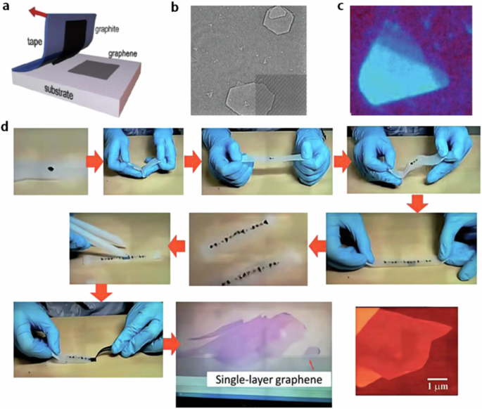
a Schematic diagram of mechanical stripping method68. b TEM images of mechanically stripped monolayer h-BN69. c Optical micrograph of mechanically detached monolayer h-BN69. d Schematic diagram of mechanical stripping of single-layer graphene based on tape70.
Other synthesis methods
Some researchers will also try to use other synthesis methods to synthesize h-BN thin films. Jang used the gas phase epitaxy growth method to epitaxy and grow multi-layer, non-folded h-BN films on the sapphire substrate (Fig. 6a). Characterization and spectral studies as well as theoretical calculations show that the grown h-BN has a single rotational orientation and AA’ stacking sequence73. Due to the high fit between h-BN and graphene, Zhang used the co-segregation synthesis method, which sandwiched the solid (B,N) layer as the precursor between the top layer of Fe and the bottom layer of Ni as the substrate (Fig. 6b). Through vacuum annealing, the B atoms and N atoms in the middle solid layer were dissolved in the metal. It is then co-segregated into the growth mechanism to form h-BN films74. Compared with the mechanical stripping method, the liquid phase stripping method (Fig. 6c) is a more efficient method for the mass production of nanosheet crystals at a low cost. Blas successfully stripped the h-BN powder into two-dimensional nanosheets in the liquid phase by mixing it in deionized water and sodium carboxymethyl cellulose salt solution75.

a Diagram of gas phase epitaxial growth h-BN on sapphire substrate73. b Fe/ (B,N) /Ni sandwich substrate co-segregation h-BN synthesis diagram74. c Schematic diagram of film synthesis process by liquid phase stripping155.
Device structures
Researchers have designed many memristors with different structures according to the differences in memristor materials and preparation processes. Common memristors are mainly composed of two electrodes and three parts of the memristor material. According to the differences in the material components of the memristor device, the memristor device can be divided into “vertical” structure and “plane” structure.
“Vertical” structure
The “vertical” structure, also known as “sandwich” structure and MIM structure, is mainly composed of top electrode (TE), functional layer and bottom electrode (BE) (Fig. 7a). The vertical structure is relatively simple and compatible with the current CMOS process. Metal is often used in the top electrode and bottom electrode, but the difference is that the top electrode usually uses active metal materials, such as Ag, Cu, Ti and Ni, while the bottom electrode usually uses inert metal materials, such as W, Pt and Au. The functional layer generally uses insulators or semiconductors with resistive effects. The metal electrode of the memristor determines the barrier height to be overcome by the electrons injected into the resistive layer, which has a great influence on the performance of the device. When the work function of the metal electrode is low, the barrier height between the electrode and the resistive layer is lower, and the carrier is easier to migrate to the functional layer. In addition to the role of the transport carrier, the memristor electrode also has an important impact on the resistance mechanism of the device. When Cu, Ag and other active metals are used as electrodes, the resistance mechanism of the device is the conductive filament mechanism76. When inert metals such as Au and Pt are used, the resistance mechanism of the device mainly includes SCLC, Pool-Frenkle and other mechanisms77,78. Table 2 summarizes the switching characteristics of h-BN memristors with different structures in recent years.

a Schematic diagram of vertical structure. b Schematic diagram of non-destructive Au/h-BN/Au intersection structure prepared by water-assisted metal transfer method39. c Schematic diagram of Ag/h-BN/ITO/PET flexible structure92. d Schematic diagram of Ag/h-BN/Pt intersection structure91. e Schematic diagram of plane structure. f The first planar memristor with an electrode Au-Pd layer and a graphene oxide layer99. g A schematic diagram of the Ag/h-BN/Ag planar structure31. h A schematic diagram of the WSe2/h-BN/graphene stack structure in the SFG-FET100. i A schematic diagram of the Ti/h-BN/Cr coil structure89.
The “vertical” structure is relatively simple and stores information by biasing the top and bottom electrodes so that the functional layer of the device changes79. In 2022, in order to reduce the influence of polymetallic ion diffusion and structural damage on the device during the preparation of the memristor electrode, J.Y.Mao used the water-assisted metal transfer method to transfer h-BN thin sheet to the Au base electrode, thus making the harmless Au/h-BN/Au cross-point structure memristor as shown in Fig. 7b. It minimizes structural damage and redundant interface defects39. Compared with devices with vacuum evaporation electrodes, the performance of the memristor prepared by this method can be significantly improved under the coexistence of non-polar switches and threshold switches (switching ratio > 107, response speed < 40 ns, holding time >20,000 s)25. In addition, metal materials are used as electrodes, and some flexible or transparent memristors use conductive glass such as ITO and FTO as the bottom electrode. For example, in 2016, Qian and Tay et al. of Nanyang Technological University reported the flexible memristor based on Ag/h-BN/ITO/PET structure as shown in Fig. 7c. ITO and PET were used instead of metal as the bottom electrode80. The memristor with this structure has been tested with a high number of repeated switches (about 550 cycles), good retention characteristics (3 × 10³s) and good bending resistance (about 750 cycles). In 2021, G.Dastgeer reported the synaptic characteristics of double-ended TS devices with Ag/h-BN/Pt intersections, as shown in Fig. 7d for neuromorphic computing applications, which showed that Ag+ mimics the bioprotruding behavior of Ca2+ through the drift dynamic touch of the shed h-BN plate migration, simulating the neuromorphic computing operation. Both short-term and long-term memory are included, and the device has a switch ratio of up to 105, leading to biological synaptic applications81. The NVRS behaviors of Al/h-BN/Pt, Al/h-BN/ITO and Pt/h-BN/ITO vertical structure devices with different electrodes were fabricated by Son. The three devices all showed RS behavior78. The switch ratio of the Al/h-BN/ITO device was 104 but showed unstable RS behavior, while the Al/h-BN/Pt device showed stable RS behavior. This may be related to the extension of O2- in the ITO electrode to the h-BN layer to oxidize the Al electrode. Villena reported the resistance switching behavior of three different composite electrode vertical structure devices: Au/Ti/h-BN/Pt, Au/Ti/h-BN/Cu, and Au/Ag/h-BN/Fe82. The types of RS behavior of the three devices are closely related to the electrodes used. When positive bias excitation is applied to the top electrode, Au/Ti/h-BN/Pt and Au/Ti/h-BN/Cu devices all show bipolar RS behavior. Au/Ag/h-BN/Fe devices exhibit threshold RS behavior. When the polarity reversal applies positive bias excitation to the bottom electrode, the Au/Ti/h-BN/Pt device no longer shows RS behavior because of irreversible breakdown due to PtX+ infiltration into the functional layer. The RS behavior of the Au/Ti/h-BN/Cu device is related to the current limiting (CL). When the CL = 1 mA, Cu ion diffusivity is large, it will form a wider and difficult-to-destroy conductive wire, which will cause the device to generate irreversible breakdown. When CL = 0.1 mA, the device has no change, and it also shows bipolar RS behavior. Au/Ag/h-BN/Fe changes from threshold RS to stable bipolar RS behavior, which means that when the device is biased and turned off, the conductive filament will interrupt itself, which has a wide application prospect in neuromorphological applications.
In practical application, the vertical structure of the memristor can be divided into common bottom electrode structure and intersection structure. The common bottom electrode structure means that the top electrode of the device shares a bottom electrode on the same planar(as shown in Fig. 7a), the preparation process is simple, and can be used for large-scale manufacturing, but the structure needs to use a probe to apply voltage during operation and testing, which will cause certain loss to the device and affect the reliability of the device. and the quality of the mask will also have a certain impact on the quality of the device when evaporating the electrode83. The intersection structure can perfectly avoid the influence of the above two factors on the device. the structure is composed of two crossed conductor wires and function layers(as shown in Fig. 7b), which do not need to share the bottom electrode, and the contact area between the metal electrode and the function layer is large. the loss of the device during testing is reduced, which is beneficial to the miniaturization and stacking of the device, but the preparation process of the intersection structure is complex and the preparation cost is high. In the actual preparation process, it may be contaminated by polymers, resulting in unstable resistance84,85,86. In addition, the crossbar structure and three-dimensional cross-array stack structure can be formed by using the intersection structure, which can greatly improve the device storage performance and reduce the storage cost.
“Planar” structure
The “planar” structure, also known as transverse structure and horizontal structure, is that the resistive material arranges double electrodes on the substrate in a planar or layered structure (Fig. 7e), and combines the resistive material with both electrodes by drip coating or spin coating, usually with atomic thinness. Compared with the vertical structure, the metal ions of the planar structure are transported through the plane rather than through the layer, and the influence of defects and grain boundaries on the leakage current will be weakened, but because of the distance between the electrodes of the planar structure, its stability is worse than that of the vertical structure. Ekiz and Urel, in order to study the electroreduction of graphene oxide in air, deposited multiple layers of graphene oxide films on a metallized glass substrate with Pd–Au films of about 10–50 nm on both sides, and made the first planar structure memristor device (Fig. 7f). However, due to the poor stability of graphene oxide flakes, there are many factors affecting the performance of the memristor device, resulting in poor stability of the memristor device despite its memristor performance87. In 2022, Wang reported the planar Ag/h-BN/Ag-based memristor shown in Fig. 7g and studied its synaptic behavior. It is found that the device has low switching voltage (<1 V), high switching ratio (>108), wide adjustable range of working current (0.1nA–1mA) and the coexistence of volatile RS when SET power is lower than 50nW and SET power is greater than 700nW. By setting different SET power, the synaptic functions of short-term plasticity (STP) and long-term plasticity (LTP) are effectively simulated, and the energy consumption of each synapse of STP and LTP is as low as 170fj and 540fj38. In 2017, Li reported that in a semi-floating gate field effect transistor (SFG-FET), a stable WSe2/h-BN/graphene nonvolatile device (Fig. 7h) is vertically stacked with WSe2, graphene and h-BN, in which WSe2 is the transmission channel, graphene is SFG, Si is the control gate, and h-BN is the dielectric layer. The power conversion efficiency of photovoltaic characteristics under the illumination of 6.8 nw is as high as 4.1%88.In addition to vertical structure and planar structure, some researchers have also fabricated other structure memristor devices. In 2019, X.Hou fabricated Ti/h-BN/Cr tube structure devices shown in Fig. 7i. This structure has a smaller device area and excellent storage performance, which can increase data storage density and reduce storage power consumption89. It has important reference in the domain of flexible wearable and 3D device sensing storage.
Due to structural differences, both vertical structure and planar structure devices have limitations and variability. Vertical structure devices have high space utilization, high integration, and short transmission paths, which can achieve higher switching speeds and lower power consumption, but because of the multi-layer stacking and interlayer alignment, more sophisticated manufacturing processes and better heat dissipation processing are required, which requires increased cost and system complexity. The preparation process of the planar structure device is compatible with the traditional CMOS process (photolithography, etching, etc.), and has a simpler and more mature manufacturing process, which is suitable for large-scale production. However, the size of the planar structure device is too large, requiring a larger chip to realize storage and integration, and due to the long current transmission path, it will lead to higher parasitic resistance and lower switching speed. The device has a higher power consumption. By analyzing the limitations and variability of the two structures, it can be seen that the vertical structure memristor is suitable for high-density storage, high-performance computing, and neuromorphic computing due to its high-density integration and excellent performance. However, its manufacturing difficulty, reliability problems, and heat dissipation challenges also limit its application range, and the future development process needs to focus on solving these problems, so that the vertical structure memristor can be applied and promoted in more fields. Due to the maturity of the manufacturing process, the planar structure memristor is more suitable for the expansion and large-scale production of the existing semiconductor technology, but its size limitations and performance optimization problems need to be paid attention to in the future development. In future memristor device designs, the advantages of both structures can be combined to achieve the best performance and integration.
Resistance mechanism
In recent years, the research on memristor is becoming more and more popular, but because of the frontier of memristor, its resistance mechanism is affected by many factors. According to the previous research, the resistance mechanism can be roughly divided into two categories: the first is based on the electrode and the resistance layer as a whole, such as metal wire and conductive filament. The second kind is based on the resistance layer itself, such as charge capture and release, atomic vacancy, defect, and so on.
Conductive filament
The conductive filament model is a widely recognized memristor resistance mechanism at present, which attributes the resistance mechanism of the memristor to the formation and fracture of the conductive filament50, the formation and breaking of conductive filaments correspond to the low and high resistance states of the memristor. which generally occurs in the vertical structure, and the formation of the conductive filament mainly depends on the selected metal electrode. active metal is generally used as the electrode, the active metal oxidizes and reduces with the metal ions near the inert metal under the external voltage to form a conductive wire. The device deals with the low resistance state. When the reverse voltage is applied, the conductive wire breaks and the device returns to the high resistance state. According to the formation of conductive filament materials, the conductive filament mechanism can be divided into three types: electrochemical metal effect, valence edge effect and thermochemical effect51,90. The number and size of conductive filaments directly determine the performance of memristor devices. The more the number of filaments is, the more concentrated the device performance is, so the formation and fracture of conductive filaments must be controlled. Usually, the formation and fracture of filaments can be effectively controlled by doping, improving preparation methods and optimizing structure.
K.Qian used CVD to grow ultra-thin h-BN films and made Ag/h-BN/Cu structure flexible memristor, and analyzed and studied its memristor mechanism, as shown in Fig. 8a. When forward bias is applied to the top Ag electrode, Ag atoms are oxidized to form Ag+ ions. After that, Ag+ ions migrate to the bottom electrode under the action of the electric field. However, due to the low mobility of cations on the h-BN film, Ag+ ions will be reduced to Ag atoms by capturing the free electrons injected from the bottom electrode after moving a short distance to form Ag conductive filaments by gathering at the top electrode. Ag conducting filaments gradually extend from the top electrode to the bottom, thus switching the memristor device to an “ON” state80. Wang in order to solve the problem of device instability caused by the randomness of conductive filament formation and growth, a device with Ag/ZnO/BNNS/Pt structure is reported. Through the study of its resistance mechanism (Fig. 8b), it is found that the migration of Ag+ in the ZnO layer is blocked, but the natural defect path in the BNNS layer is the significant increase in the mobility of Ag+ in the BNNS layer, due to the different transmission characteristics of the two layers. The formation and fracture position of the conductive filament is limited to the ZnO/BNNSs interface. Compared with the ZnO-based devices, the switching parameters, uniformity and stability have been greatly improved. This study has opened up a new way to improve the stability of the memristor91. In 2019, Zhu used graphene clamped multilayer h-BN stack to fabricate 5um × 5um cross-point Au/Ti/G/h-BN/G/Au structure devices. The device has three stable and easily distinguishable resistance states shown in Fig. 8c. This is because graphene limits the ion exchange between metal electrodes and h-BN, resulting in an intermediate state of S-LRS between HRS and LRS. Moreover, the device can switch between every two or three resistive states by adjusting the limiting current (CL) and reset voltage (VRESET), which is not observed in the memristor with the same structure but a different size and the same size without graphene intercalation. This study promotes the development of three-state adjustable two-dimensional material memristor92.

a Based on Ag/h-BN/Cu device transmission mechanism80. b Based on Ag/ZnO/BNNSs/Pt device switching mechanism91. c Schematic diagram of MIM unit structure of three resistive states of Au/ Ti/G/h-BN/G/Au devices92.
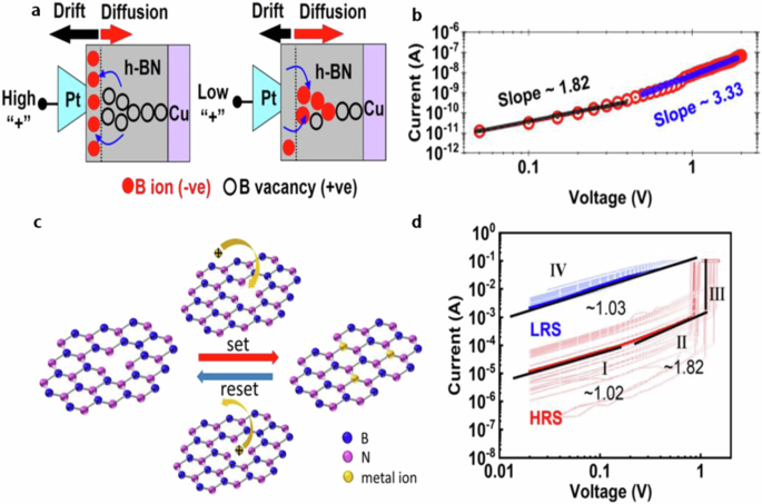
Vacancy migration
In addition to metal ions, vacancies also play a very important role in the resistance process of memristor devices. The vacancy is caused by the defect vacancy in the resistance layer and the migration of ions under the action of the electric field. generally, the oxygen vacancy is the majority. The vacancy can be traced back to 2008 when the memristor was first found to explain its resistance behavior. Hou fabricated Ti/h-BN/Cr coil structure memristor by self-winding technology in 2019. The device has a switch ratio of 103 and has a smaller footprint, higher VSET and lower programming current. Through the study, the resistance principle can be attributed to the migration of boron vacancies (Fig. 9a): there are grain boundary defects in polycrystalline h-BN films grown by CVD. The number of boron vacancies in these defects is very abundant89. When a forward bias is applied to the Ti electrode, the boron ions in the h-BN resistance layer migrate to the Ti/h-BN interface with the assistance of lattice defects and keep the boron vacancies at the original position. with the increase of the number of boron vacancies, the boron vacancies reach the Cr electrode to form conductive filaments and switch the device from HRS to LRS. In 2022, Li reported the RS switching mechanism of the Au/h-BN/Au memristor based on monolayer h-BN at the thinnest limit. Figure 9b shows that the van der Waals gap between the Au electrode and the monolayer h-BN ensures the formation of the HRS, and the Au atoms pass through the h-BN through the boron vacancy (VB) to form a complete conductive filament and fill the van der Waals gap, thus switching the device from HRS to LRS93. This study provides a key working picture for the thinnest limit of memristors and a new reference for the development of advanced ultra-miniaturized memristors.

a The formation process of conductive filaments in Ti/h-BN/Cr coil structure92. b The schematic diagram of Au/ monolayer h-BN/Au devices and the formation of conductive filaments by Au atoms through VB93.
Charge release and capture
In addition to the above two kinds of ion migration and vacancy migration, there are some memristor device resistance mechanism related to charge effect, this device mainly relies on electron conduction, thus forming resistive behavior. The memristor based on charge capture and release is usually related to the trap inside the resistive layer of the device. When the carrier is captured by the defect in the resistive layer, the energy distribution of the trap in the energy band will change, resulting in the conversion between high and low resistance states. When two-dimensional materials such as h-BN, GO and MoS2 are used as the resistance layer, the charge release and capture mechanism can be observed94,95,96,97,98.
In 2018, Ranjan used CVD to grow multilayer h-BN on Cu substrates and studied its switching characteristics using the Pt tip of Conductive Atomic Force Microscopy (CAFM) as the top electrode99. The results show that the formation and migration of boron vacancies are more favorable than nitrogen vacancies. The resistance mechanism shown in Fig. 10a shows that the forward high voltage is applied. B-drift to the Pt tip accumulates on the surface of h-BN in the form of sheet charge to form boron vacancy inside h-BN. Boron vacancy wire makes the device transition from a high-resistance state to a low-resistance state. When the polarity is switched to a low negative voltage, the B-diffuses from the top layer of the h-BN near the Pt tip to the h-BN stack, which passivates the boron vacancy wire, and then annihilates, and the device transitions from the low resistance state to the high resistance state. The double logarithmic I–V fitting of the LRS when the current compliance (Icomp) is 100 nA (Fig. 10b) shows that the conduction of the device is controlled by space charge limited conduction (SCLC) when the applied voltage is small (<0.5 V), and when the applied voltage increases (>0.5 V), the conduction of the device is assisted by carrier jumping through traps between multiple layers of h-BN. Therefore, the overall conduction of the device is controlled by traps and defects in the h-BN/Cu stack. In 2022, Li et al. used molecular beam epitaxy (MBE) to grow monolayer h-BN and fabricated Au/monolayer h-BN/Ni devices, and studied their resistance switching performance100. The resistance mechanism shown in Fig. 10c shows that the RS behavior of the device is not accompanied by the Forming process. When the device is switched from HRS to LRS, the boron vacancy in the monolayer h-BN will be filled by nickel ions due to the migration of Ni ions, resulting in conductive filaments and ohmic-like conductivity. when negative bias is applied, the conductive filaments are subjected to ion diffusion or Joule melting caused by electric field, so that the device is converted to HRS. Through the I–V characteristic diagram of HRS and LRS drawn on double logarithmic scale (Fig. 10d), it can be seen that in the region I of HRS, the slope of I–V curve is 1.02, and the device works in the direct tunneling region, which is ohmic conduction. With the increase of voltage, the current increases sharply, the slope of the h-BN I–V curve increases, the charge inside the h-BN resistance layer in region II and region III begins to fill traps, and the conductive wire begins to form slowly. Once all traps are filled, carriers can freely pass through the h-BN layer, and finally form a conductive channel, and the device is converted from HRS to LRS, which is very consistent with the previously reported characteristics of SCLC resistance mechanism.
a Schematic diagram of switching mechanism of Pt/h-BN/Cu device99. b Double logarithmic I–V curve of the device when the adaptation current is 100 nA99. c Schematic diagram of the resistance switch of single-layer h-BN device, the metal ion fills the boron vacancy under the action of electric field at SET, and the resistance state becomes LRS; the metal ion is subjected to Joule thermal collapse at RESET, resulting in CFs fracture and the resistance changes back to HRS100. d Fitting of the I–V curve of HRS and LRS on the logarithmic scale100.
Although the resistive mechanism of the memristor device has helped in the development and application of the memristor, there are certain problems in the repeatability, stability, and reliability of the memristor, which limit the further development of the memristor: In the conductive filament mechanism, the randomness of the formation and fracture of the filament will lead to the difference in the position, shape and size of the filament each time the resistance state of the device is switched, and with the increase of the switching times, the conductive filament will become thinner and thinner, and the resistive material will age, which will lead to the change of the resistance value of the device, and then affect the repeatability, stability and reliability of the device. At the same time, the formation and fracture of filaments at low temperature or high resistance takes a certain time, which also limits the read and write speed of the device, and does not meet the needs of high-speed storage and calculation in specific situations. The vacancy distribution and migration path in the vacancy migration mechanism also have some randomness, and the microscopic process of migration is difficult to accurately control, which will lead to different resistance state changes in the device under the same experimental conditions, affecting the repeatability and consistency of the device. In a high-temperature environment, some vacancies not only migration speed fast, but the distribution of vacancies may also change due to the REDOX reaction inside the material caused by high temperature, further affecting the stability and reliability of the device, which can not meet the needs of high-temperature data storage. Similarly, due to the random distribution of trap states in the material, and the release and capture of charge each time will lead to different field strengths in different areas of the material, which will also lead to the instability of the device when the resistance state is switched. Part of the charge in the trap state for a long time in high temperature environment will also cause the device resistance state cannot be reset, affecting the reliability of the device. The limitations discussed above indicate that there are still many challenges to be met in the further development of memristors, and further research and optimization of memristors in the aspects of material science, device design, and manufacturing process are needed in the future, and more discussion of its resistance mechanism is needed to achieve better performance and more reliable performance in a wider range of application scenarios.
Functional modification based on h-BN functional layer
At present, the main problem facing memristor devices is how to improve the stability of the device performance. The performance of the memristor can be improved by modifying the resistive material. Functional modification is the use of physical or chemical direction to change the structure of the material on the basis of not changing the overall structure of the material, so as to improve the overall performance of the material, and even make the material show new physical or chemical properties.
Defects and doping
It is worth noting that because h-BN is not a perfect crystal, its internal defects will affect the performance of h-BN. Lin studied the calculation of the interface between metal and h-BN with different defect types, and the research results showed that various defects played an important role in improving the stability and electrical conductivity of metal/h-BN101,102. As shown in Fig. 11a, b, the charge of defenceless h-BN supported by Cu(111) transferred from metal to h-BN is only 0.01e, but after the introduction of point defects such as VN and VB, the transfer charge increases to 0.45e and 1.34e respectively, thus forming a gap state near the Fermi level. The metal/h-BN has strong catalytic activity. Lyalin found that defects can also improve the catalytic activity of pure h-BN. When NB and BN defects are introduced, the band gap of h-BN monolayers decreases to 3.27 eV and 1.45 eV, and defect levels appear. With the introduction of VB and VN defects, h-BN has the properties of both a P-type semiconductor with spin-down electrons and an N-type semiconductor with spin-up electrons, forming a conductive network in h-BN103. Ageev also reported the X-ray-induced modification of h-BN104. After X-ray irradiation, defects were generated in the h-BN film and impurity atoms on the surface of h-BN were removed, thus significantly changing the electronic structure and composition of the surface of h-BN. Moreover, by increasing the current and lowering the threshold, the surface of h-BN was improved. The electron field emission characteristics of h-BN films are also greatly improved.

a Optimization of h-BN nanosheets supported by Cu(111) and h-BN nanosheets with VN and VB defects102. b Charge transfer from metal to different defects102. c, f Optimization of Al-doped and P-doped h-BN nanosheets110. d HOMO spectrum of P-doped h-BN nanosheets, and HOMO energy level transferred to P atom110. g LUMO spectra of Al-doped h-BN nanosheets, and LUMO energy levels transfer to Al atoms110. e, h Partial DOS diagram of P-doped and Al-doped h-BN nanosheets110. i I–V curve of Ti/h-BN/CuNi structure device111. j Grain diagrams in h-BN films of Ti/h-BN/Cu(left) and Ti/h-BN/CuNi(right) structured devices from the top perspective. Compared with h-BN films grown directly by Cu foil, the h-BN films grown by Cu foil doped with Ni have larger grains and lower grain boundary density111.
In addition to defects affecting the performance of h-BN, doping is also an effective means to regulate the electronic structure and catalytic activity of h-BN, among which C doping is the most common105,106, and C can replace B and N atoms in h-BN. In 2015, Zhao found that doping a single C atom into the h-BN monolayer can obtain higher spin and charge density and reduce the energy gap107. However, when C replaces B atoms, C requires additional drive energy due to its high activity, which is harmful to ORR, in contrast, when C replaces N atoms, it exhibits appropriate activation, promoting the spontaneous quad circuit of ORR. Tian found that doping C on the Co substrate could increase the adsorption energy of B and N, thereby reducing the diffusion activation energy, promoting the nucleation and lateral growth of two-dimensional h-BN layer, and eliminating the formation of columnar layer108. As reported by S. Caneva, doping Si in Fe substrate can reduce the nucleation density of grown h-BN, thus growing a larger h-BN film109, which is of great significance for enhancing the controllable expansion growth of two-dimensional materials. Hosseinian found that after doping non-metal P and metal Al, the electronic properties of h-BN were changed (Fig. 11c, f). After doping P, the HOMO energy level of h-BN was significantly changed, and the HOMO was transferred to the P atom (Fig. 11d). After Al doping, the LUMO energy level of h-BN changes significantly, and LUMO is transferred to Al atom (Fig. 11g). The DOS analysis shown in Fig. 11e and Fig. 11h shows that the contribution of P atom in HOMO level is about 80%, and that of Al atom in LUMO level is about 85%, which indicates that. P doping can significantly improve the electrochemical performance of h-BN, while Al doping reduces the corresponding electrochemical performance110. Lanza reported the Ti/h-BN/CuNi structure memristor device prepared by Ni-doped h-BN111. The I–V curve shown in Fig. 11i) shows that when positive voltage is applied, the device exhibits bipolar RS behavior with lower HRS current, which may be due to larger grains in the Ni-doped h-BN layer, reduced internal defects, and a small number of conducting nanowires and grain boundaries formed (Fig. 11j).
Functional group modification
For most h-BN, the B–N bond is very strong due to its extremely high chemical stability, and there are no modified functional groups in the h-BN structure for bonding112. The existing modification methods often can not change the B–N bond well. The modification process of H-BN all involves the opening of B–N bond. When the functional group bonds with B or N atom, the corresponding group should also be connected to the unpaired N or B atom to balance the total charge113,114,115. Therefore, it is very necessary to explore new methods to modify B–N bond, so as to realize the functional modification of h-BN. Studies have shown that the introduction of –OH and –NH2 at the edge of h-BN during its preparation process can make h-BN modified116. In addition, h-BN can be further modified by grafting more complex functional groups/molecules to change its surface chemical/physical properties, as shown in Fig. 12a. Weng grafts a large number of different functional groups on the surface of h-BN, so that h-BN has more active sites and realizes functional modification117. At present, there are many modification methods for h-BN. For example, ball-milling and ultrasonic methods can be used to modify h-BN groups such as –OH, –OR118, –NH2119,120, –R121 and –X122, among which –OH and –NH2 are the most widely used. Compared with other group modification methods, hydroxyl group modification is considered to be the most promising h-BN modification method.

a Schematic diagram of h-BN surface grafted with different functional groups to achieve functional modifications117. b Schematic diagram of h-BN functionalization by air plasma131. c Diagram of SA modified h-BN surface25.
At present, the strategy of changing the electronic properties of h-BN surface structure by tube energy group modification has been widely studied in the fields of catalyst, biological carrier, sewage purification, etc., but there are few reports in the field of memristor. Therefore, this part mainly introduces several typical methods of h-BN surface covalent bond modification. Pakdel treated h-BN nanofilms with air plasma to achieve the surface hydroxylation of h-BN123. Through further research, Pakdel proposed the functionalization mechanism shown in Fig. 12b: first, covalent bonds are formed at the active edges and defects, and then the reactive substance attacks the electron-deficient boron atom and the electron-rich nitrogen atom through the Lewis acid–base interaction, and finally causes the B–N bond to break and form a new bond. Luo mixed h-BN with SA solution in the method shown in Fig. 12c to achieve the surface modification of h-BN particles25. After modification, the crystallinity of h-BN remained unchanged, but the agglomeration problem of h-BN was reduced, which was also beneficial to the peeling of h-BN particles. Lin used ultrasonic method to achieve h-BN hydroxylation, and treated h-BN in a water bath for 8–24 h. After centrifugation, the massive h-BN nanosheets were stripped into single-layer h-BN nanosheets. In the ultrasonic water bath environment, the h-BN nanosheets were broken, and the B–N bond at the defect site was attacked by oxygen atoms, thus hydroxylation was achieved. The infrared spectrum test results show that the h-BN plate contains an -OH absorption peak, which proves the completion of hydroxylation124. Ito uses plasma in the solution to modify the surface of h-BN without adding any acid or base125. Studies have shown that the modification increases the defect density in the h-BN layer, and the number of hydroxyl groups also increases with the increase of modification time. Bai prepared hydroxylated boron nitride nanosheets (HO-BNNS) by stripping h-BN with hydroxide126. The results show that HO-BNNS, as a water-based lubricant, has a higher wear diameter, average friction coefficient, wear amount and thermal conductivity than the original h-BN. The thickness reaches atomic level and the dispersion is good. It is a promising water-based lubricant and additive. These modifications affect the ionic mobility and band structure of h-BN. Therefore, it is necessary to further study the resistive switching properties of functional group modified h-BN as a functional layer.
Polymer modification
Polymer modification refers to the addition of inorganic or organic substances to polymers by physical and mechanical methods, or the blending of different types of polymers, or the copolymerization, grafting and crosslinking of polymers by chemical methods, so as to reduce the cost of materials, improve the molding processing performance or final use performance. In electricity, magnetism, light, heat, sound, combustion and other aspects are endowed with unique functions and other effects. In 2020, Ge inserted a PMMA interfacial polymer layer between the monolayer h-BN and the top electrode to prepare the Ag/PMMA/h-BN/Cu structured device shown in Fig. 13a, which has low operating voltage, high switching ratio, and long hold time (Fig. 13b). It can also limit the size of conductive filaments and prevent the formation of excess conductive filaments on the bottom Cu electrode127; Fig. 13d shows that without PMMA intercalation, since both Ag+ and Cu2+ are active, after voltage is applied to the device, both Ag+ and Cu2+ enter the h-BN layer to fill the B vacancy and form a conductive channel, which changes the resistance state of the device into LRS. However, because the top electrode is directly connected to h-BN, the conductive channel is larger. This means that the LRS resistance is lower and the RESET current is higher, making the CFs difficult to break down, resulting in devices that are difficult to reset to HRS. After the PMMA polymer layer is inserted, Ag+ and Cu2+ no longer fill the B vacancy easily under the action of electric field due to an extra layer of polymer between the top electrode and h-BN, thus preventing the formation of CFs in the reset, so that the device can be reset from LRS to HRS, improving the yield and reliability of the device. This study presents a new strategy for scalable interface engineering and reveals the application prospect of this method in large-scale integrated flexible memory. In order to improve the thermal conductivity of h-BN, Shen mixed polydopamine (PDA) with h-BN powder and studied the biological modification of h-BN128. It was found that after mixing PDA with h-BN, an effective thermal channel was formed inside it (Fig. 13c), the thermal conductivity was significantly improved, and the modification method was convenient and environmentally friendly. It can be used for mass production of high thermal conductivity composite materials. In 2016, Siddiqui mixed h-BN with PVOH (Fig. 13f) to produce Ag/h-BN/PVOH/ITO flexible device (Fig. 13e), which showed good non-volatile, repeatable and bipolar RS behavior at low current compliance and low operating voltage. With a switching ratio of up to 4.8 × 10², this study demonstrated excellent durability and mechanical stability in 1500 bending cycles with different bending degrees, broadening the understanding of memory behavior in composite nanomaterials mixed with two-dimensional materials and polymers81.
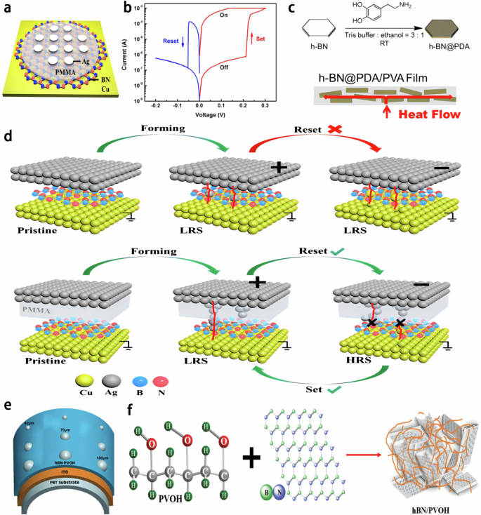
a Ag/PMMA/h-BN/Cu structure diagram127. b LRS and HRS distribution for 800 cycles of the device127. c Schematic diagram of the mixing of PDA and h-BN (top) and the formation of hot channels inside the film after mixing (bottom)128. d Schematic diagram of the resistance switch of the device without PMMA and after PMMA insertion. Ag+ and Cu2+ enter the single-layer h-BN without PMMA insertion, and the device is difficult to reset to HRS. After insertion, the PMMA layer prevents the formation of Cu wires during reset and effectively controls the growth of conductive wires127. e Schematic diagram of Ag/h-BN-PVOH/ITO device structure81. f Mixing diagram of h-BN and PVOH81.
Heterogeneous structure modification
h-BN exhibits a strong van der Waals force (vdW) together with other layered materials, so it is very necessary to study the performance of memristor devices based on h-BN heterostructure. At present, the research on h-BN heterostructure is mainly grapheme.
Li reported a heterostructured programmable p-n junction based on WSe2/h-BN/Gr, where part of the WSe2 channel is located on top of the graphene, separated by about 20 layers of h-BN88. Charging and discharging of the floating gate can be accomplished by applying a high drain pulse to a simple two-ended device, thus achieving a switching ratio of about 104, thus paving the way for the design of non-volatile memory devices based on vdW heterostructures. Deng designed a novel G/h-BN/G/SiO2/Si heterostructure memristor device shown in Fig. 14a by sandwiching single crystal h-BN between two thin graphite layers129. The heterostructure of graphite and h-BN can be clearly seen in the optical microscope image shown in Fig. 14b. The I–V curve shown in Fig. 14c indicates that the device has stable RS behavior and a switching ratio of more than 103. Pan prepared the Ti/MLG/h-BN/MLG/Au heterostructure device shown in Fig. 14d by inserting a layer of multilayer graphene between the h-BN and the metal electrode111, the XTEM image shown in Fig. 14e shows a thick two-dimensional layered heterostructure stack, and Fig. 14f shows that, compared with the device without MLG inserted, After MLG insertion, the forming voltage of the device is increased to 8 V, the RESET process is also sharper, the variability of the device is reduced, the data retention time is increased to 4 × 10⁴ s, and the switching ratio is also increased to 104. Zhu prepared an Au/Ti/G/h-BN/G/Au isostructured memristor, which can modulate the LRS and conductivity of the modulator part by adjusting the limiting current (CL)92. When CL = 5 mA is used, the device switches between HRS and LRS, and when low CL = 0.5 mA is used, the device switches between HRS and LRS. The device switches between HRS and low-conductivity LRS (S-LRS), which is formed by ion exchange between graphene-confined metal electrodes and h-BN, and when CL = 1 mA is used, stable RS is detected to exhibit three resistance states (i.e. HRS, S-LRS, and LRS). This study promotes the development of three-state operable and tunable two-dimensional material memristors. Suzuki successfully grew an H-BN layer on a single carbon nanotube and carbon nanotube bundle by dry spinning (Fig. 14g), and successfully prepared the h-BN/CNT heterogeneous memristor device as shown in Fig. 14h. The electrical transport test observed obvious memristor behavior in the device. Studies have shown that the resistance behavior of the device is caused by the disordered amorphous carbon structure between the h-BN layers. As shown in Fig. 14i, in the initial state, the h-BN layer is separated from the dielectric layer of carbon nanotubes and amorphous carbon, and the device is in HRS. The carbon atoms provided by amorphous carbon enter the h-BN layer to form a conductive channel, resulting in the transition from HRS to LRS130.

a Structure diagram of G/h-BN/G device129. b Optical images of G/h-BN/G devices129. c G/h-BN/G device I–V curves129. d Structure diagram of Ti/MLG/h-BN/MLG/Au device111. e XTEM images of Ti/MLG/h-BN/MLG/Au devices111. f I–V curves of Ti/MLG/h-BN/MLG devices111. g h-BN diagram of growth of single carbon nanotubes and carbon nanotube bundles130. h h-BN /CNT memristor structure diagram130. i Schematic diagram of resistive mechanism of h-BN/CNT memristor130.
In general, the above four methods are currently common technical means to achieve h-BN-based memristor functional modification, each method has its own advantages, but there are certain limitations, in order to more in-depth discussion of various modification methods, Table 3 summarizes and compares the advantages and limitations of the above modification methods: The introduction of defects and doping can change the electronic structure inside h-BN and regulate the conductive channel of h-BN memristor, but it is difficult to doping uniformly in h-BN, the doping concentration is difficult to control, and the electrical performance of the device is difficult to maintain consistency. The insertion of polymer can improve the adjustability of the h-BN layer, increase the flexibility and mechanical stability of the device, and optimize the conductive channel of the device to adjust the resistance characteristics by changing the type and thickness of the polymer. However, the thermal stability of the polymer is poor, and the performance is easy to degrade or even lead to material degradation at high temperatures. Some polymers have weak electrical conductivity, and there may be poor contact between the interface and h-BN, which may lead to the charge transfer efficiency of the memristor and affect the device performance. The introduction of functional groups can regulate the surface chemical properties of h-BN, thus regulating the charge transfer and resistance mechanism of the device, and increasing the interface charge injection efficiency. However, the introduction of some specific functional groups requires precise control of the chemical reaction conditions, which leads to complex modification processes and poor repeatability, making it difficult to achieve consistency in large-scale preparation. Combining h-BN with other two-dimensional materials to form a heterogeneous structure can enhance the electrical conductivity, optimize the electrical characteristics, and further improve the performance of the memristor. However, the construction of high-quality two-dimensional heterogeneous structures requires a more precise preparation process, which increases the preparation cost and process complexity, and the thermal expansion coefficient and thermal conductivity of different two-dimensional materials are greatly different. It may lead to the accumulation of interfacial stress and affect the thermal stability and long service life of the device.
Application prospect of h-BN memristor
As a rapidly developing two-dimensional material, h-BN’s morphology, structure, and composition directly affect its performance. Due to its many special properties, such as high temperature oxidation resistance, high stability, flexibility, corrosion resistance and high thermal conductivity, h-BN has been widely used in insulation, high temperature resistance, catalyst, ceramics and other fields2. The emergence of memristor provides a new idea for the development of storage technology, so the application field of h-BN-based memristor is not only information storage but also can be combined with circuits, computer processing, and other fields, thus widening the application prospect of h-BN.
Artificial synapses based on h-BN memristor
Since the density of the memristor array can reach the density of synapses in the biological nervous system, and the properties of the memristor resistance depending on its past state are similar to the way neural synapses work in the brain, it can be used to simulate synaptic connections in the human brain and for related studies on neuromorphic chips for neurodynamics131,132. In order to simulate synapses, the artificial memristor device unit must have simulated switching behavior. The memristor has a relatively smooth SET and RESET process (Fig. 15a), so it is suitable for simulating synapses and studying synaptic behavior133,134.

a Schematic diagram of similarity between the structure of memristor devices and synapses133. b The change of Ag/h-BN/Pt flexible synaptic device conductance with the number of pulses81. c Enhancement and inhibition characteristics of Ag/BN/Pt memristor devices under 500 pulse stimulation136. d Schematic diagram of neural networks, including 400, 100, and 10 input, hidden, and output neurons, respectively136. e Pattern recognition accuracy of Ag/BN/Pt devices (close to ideal devices)136.
The Ta/h-BN/Pt devices prepared by Wu have continuously adjustable conduction states, which can simulate the long-term enhancement and inhibition behavior of the synaptic weights of organisms135. Dastgeer prepared the Ag/h-BN/Pt flexible bulge device and simulated the neuromorphic computing operation81. It was found that the conductance of the device was converted from STP to LTP as the number of pulses increased (Fig. 15b), which corresponds to the Atkinson–Shiffrin model on human brain learning. This suggests that threshold switches with large switching ratios can lead to biological synaptic applications, and this study opens the way for the application of memristor devices with two-dimensional flexible h-BN materials in neuromorphism. Khot prepared the Ag/BN/Pt memory device to explore its synaptic characteristics. As shown in Fig. 15c), the device simulated the synapse-weight modulation effect under 80 enhancement pulses and 80 suppression pulses at 0.1 V, and realized the gradual change of memristor due to enhancement and suppression under 500 cycles of pulse stimulation. This shows that the Ag/BN/Pt device can simulate basic biological synaptic processes, and Khot obtained a 20 × 20 pixel handwritten digital image from the MNIST database through a MATLAB simulator, using 400 input neurons, 100 hidden neurons, and 10 output neurons to recognize the digital image (Fig. 15d). The potential of devices in the field of machine learning is further explored136. The test results show that the recognition accuracy of the prepared device in the neural network simulation reaches 90.8% (Fig. 15e), showing that boron nitride is an excellent 2D material for easy application in neuromorphic computing.
There is one thing to note about the use of memristors in synapses. Despite extensive research on the application of memristors in the synaptic field, there are still limitations in many aspects, We still have to be serious about it: first, linearity and symmetry. When applied to synapses, memristor need to simulate the adjustment process of synaptic weights. Because the change of resistance in practical applications is often nonlinear and asymmetrical, it will lead to convergence difficulties in training neural networks, thus affecting the effect of deep learning. The second problem is the fitness between the neural network training algorithm and the hardware. Most of the existing neural network training algorithms are designed based on digital circuits, and memristor is a simulator. In the training process, it is necessary to formulate a suitable algorithm according to the characteristics of the memristor (such as nonlinear, hysteresis effect, etc.), otherwise the advantages of the memristor can not be fully utilized. Finally, there is the problem of noise and signal recognition accuracy. The memristor is easy to be affected by the noise of the device and introduces the wrong signal, which affects the training result of the neural network and limits its application in high precision. These problems limit the wide application of memristors in large-scale synapses, and future development requires further innovative research in material structure, device engineering and algorithm design to fully unlock the potential of memristors in brain-like computing137.
Sensors based on h-BN memristor
Based on previous studies on memristors, it has been well demonstrated that memristors can be applied to sensing devices138,139. As we all know, the resistance change of memristors is caused by the formation or fracture of vacancy filaments. Due to its memristor characteristics, h-BN materials are also used to build gas monitoring systems, and the corresponding devices using h-BN as the functional layer have stable storage behavior, such as low threshold voltage, stable holding time, clear resistance state, and high switching ratio140. As shown in Fig. 16a, the absolute adsorption energy of h-BN for NOX gas is larger and more favorable than that of other gases. Therefore, h-BN has high selectivity and response characteristics for NOX gas, Chae et al. used h-BN as the functional layer to construct a gas sensor based on memristor array as shown in Fig. 16b. The sensor was applied to the NO gas detection system embedded in the neural network141, It is found that the h-BN memristor based NO sensor array has a high response of 8922 and a low detection limit of 0.5ppm at room temperature, and the error rate is reduced by 17 times compared with a single device. These results indicate that the response, selectivity, test data and accuracy of the device to NO gas are significantly improved, and the LRS and HRS processes of the memristor were corresponding to the reaction and recovery mechanism of the gasser device. The system could quickly and accurately detect the concentration of NO gas, and its operating power consumption was only 3.7nW. The following year, Lee reported a new prediction method for discontinuous NO gas. He combined the gas sensor of the Ti/h-BN/Pt memristor shown in Fig. 16c with the neural network to build a gas prediction model (Fig. 16d) to study the response of NO gas in discontinuous flow142. The research showed that this model could accurately predict the discontinuous NO gas concentration. The margin of error was just 5.6 percent. This method is expected to be used to analyze and predict the response characteristics of gas sensors in various fields, such as artificial nose system.

a Adsorption energy of h-BN for different gases. b The lower left is the diagram of NO gas detection system based on h-BN memristor, the upper left is the LRS and HRS corresponding to the reaction and recovery mechanism of gasia furnace, and the right is the real-time monitoring model of NO gas built by neural network141. c Structure diagram of Ti/h-BN/Pt memristor used as NO gas sensor142. d The principle diagram of NO gas monitoring model based on memristor gas sensor combined with neural network142. e Structure diagram of Cr/Ag/h-BN/Cr/Ag memristor for biosensing systems143. f (i-ii)Schematic diagram of the basic principle of a biological damage sensing system and (iii)Schematic diagram of the basic principle of memristor based artificial damage sensing system143.
In addition to the above gas sensors, h-BN-based memristor devices can also be applied to biosensing systems, Ding connected the prepared Cr/Ag/h-BN/Cr/Ag memristor (Fig. 16e) with the triboelectric nanogenerator, successfully designed a self-powered damage sensing system capable of sensing external stimuli and simulated the characteristics of “relaxation” and “abnormal pain” of biological nociceptive receptors143. Fig. 16f compares the basic principles of biological damage sensing system and artificial damage sensing system: As shown in Fig. 16f (i-ii), when biological nociceptors receive electrical signals generated by external stimuli, they will compare the intensity of the signal with their own threshold to determine whether to generate action potential. When the intensity of the signal is greater than the threshold, action potential will be generated and transmitted to the brain through the spinal cord without causing pain; otherwise, action potential and pain will not be generated. In the artificial sensing system based on the h-BN memristor device shown in Fig. 16f (iii), input voltage pulses are used to simulate external stimuli. When the input pulse is greater than the threshold voltage, the memristor device switches from “OFF” state to “ON” state, and the output current indicates the sensing system’s perception of the stimulus. On the other hand, when the input pulse is less than the threshold voltage, the memristor device remains “OFF” state without output current. The research provides an important reference for constructing low-power sensing system.
Logic circuit based on h-BN memristor
Compared with traditional memory, memristors have lower power consumption, faster response speed and larger switching ratio, and can be used as logic gates in the field of logic systems144,145,146,147. In 2009, Xia used nanoimprint technology to integrate the memristor on the CMOS platform, which is the first hybrid integrated circuit of memristor and CMOS in the world, which shows that the memristor has good compatibility with CMOS147. This result provides a new direction and idea for the application of h-BN memristor in the field of logic system.
Meng discovered that a BN-based memristor array has the function of a memory and algorithmic logic unit (ALU), and prepared an ITO/h-BN/TaN memristor device as a memory algorithm logic unit (MALU), combining the memory and ALU functions (Fig. 17a), and then combined with traditional resistors. A non-volatile logic storage circuit for digital memory computing (Fig. 17b, c) is constructed, and basic IMP and NAND Boolean logic gates are successfully implemented, providing potential possibilities for building digital memristor computing systems with zero static power and high efficiency148. Kumar prepared a multi-layer h-BN-based memristor cross array, which exhibited simulated bipolar resistive switches, combined it with CMOS circuits to build the hybrid architecture based on extreme learning machine algorithm (ELM) shown in Fig. 17d and applied it to edge computing. The research shows that the hybrid architecture overcomes the area and memory wall problems of CMOS circuits. It is versatile enough to be used for audio detection, image classification, and other edge computing tasks where power and area are strictly limited149. Pazos used CVD to produce Ag/h-BN/Ag structure memristor, which showed extremely stable random telegrams noise (RTN) signals with very low power consumption at a bias voltage of 70 mV. Then, the memristor was connected with a commercial microcontroller to build a true random number generator (TRNG) circuit as shown in Fig. 17e. It is found that even if the RTN signal at the input is interrupted for 20 seconds, the circuit can produce a signal with high randomness and high throughput150. Zhu used CVD to prepare Au/Ti/h-BN/W memristors and transferred them to the back-end interconnect of silicon microchips containing 180 nm node-CMOS transistors, and prepared highly integrated 2D-CMOS hybrid microchips with 1T1M structure. The device was tested and found that the CMOS transistor provided excellent control over the current of the hexagonal boron nitride memristor. Compared with the independent h-BN memristor and the h-BN memristor mixed with two-dimensional materials, the electrical performance of the mixed h-BN memristor with the CMOS transistor was better, and the device switching voltage was between 1V-5V. Much lower than other two-dimensional materials based devices. This research drives the further development of integrated 2D materials in microelectronics and applications151.
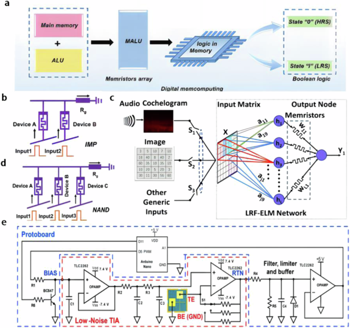
a BN memristor array as MALU. Schematic diagram of combined storage and ALU functions (memristor HRS for logic 0, LRS for logic 1)148. b, c Based on the logic circuit built by BN memristor and traditional resistors, IMP logic gate and NAND logic gate (devices A, b and c are memristors) are realized148. d A hybrid architecture diagram based on ELM algorithm based on the combination of h-BN memristor cross array and CMOS circuit149. e Schematic diagram of a TRNG circuit constructed by connecting an h-BN memristor to a microcontroller. The RTN current signal generated by the memristor is converted into a voltage through a transresistance amplifier, and its output is fed back to the analog input of the microcontroller (A1)150.
Summary and outlook
In this paper, the application progress of h-BN in memristor devices is reviewed. Five aspects of h-BN film preparation, structure of memristor devices, resistance mechanism, functional modification and application prospect are analyzed and summarized. It is found that the performance of the h-BN memristor is affected by many factors, such as the thickness of the resistive layer, the type and thickness of the electrode, and the structure of the device. At the same time, the resistive mechanism of h-BN memristor is mainly metal ion, boron vacancy migration, space charge limited current. Through the analysis of the resistive mechanism, it is found that the microstructure of the resistive layer, electrical properties, electrode types and other factors will affect the resistive mechanism of the device. h-BN has a hexagonal structure similar to graphene, due to its high mechanical strength, good chemical stability and transparency, good insulation and thermal conductivity and many other unique properties, h-BN-based memristor has a very broad development and application prospects. The research of h-BN is of great theoretical significance and application value for the next generation of wearable and foldable flexible and transparent non-volatile storage devices. However, the relationship between the performance of h-BN memristor and electrode material, device structure and resistance mechanism is still unclear, which hinders the improvement of h-BN memristor performance and the development of the device. To study the factors affecting the resistive mechanism of h-BN memristor has become a key problem to be solved to improve the performance of the device. In the future, the research on h-BN memristor can be in-depth from the following aspects:
The first is to optimize the growth and transfer methods of h-BN films. CVD is currently a commonly used method for preparing h-BN films. Through the analysis and research of the preparation method of h-BN, we found that although wafer size h-BN films were prepared by CVD method, dehumidification would occur at 800°C when metal foil was used as the substrate in the traditional method, and it was very difficult to grow h-BN films on metal foil. In this case, wet transfer may result in polymer or metal residues, increasing the number of defects. At present, there is no relevant research that can simultaneously solve the problems of h-BN wafer size growth, metal substrate high-temperature dehumidification, pollution transfer, and so on. In order to solve these problems as much as possible, in the future memristor research, it is possible to consider the combination of improving the transfer process, introducing the inorganic buffer layer of h-BN grown in CVD, exploring the in-situ CVD growth, etc., to provide effective support for the high-quality preparation and high-performance application of h-BN thin films.
The second is to further study the resistance mechanism of h-BN memristor. Due to the influence of device structure, electrode material, preparation method and research method, the resistance mechanism of h-BN memristor has not been fully defined, which affects the further performance optimization of the device. In the future, h-BN memristor research process, more advanced research methods need to be used to further study h-BN memristor devices prepared with different structures, different electrode materials, and different preparation methods. For example, surface probe, XPS, experimental characterization and theoretical simulation can be combined to further analyze the switching mechanism of h-BN memristors with different defects and structure regulation, so as to make the resistance mechanism of the device more clear.
The third is to optimize the device stability of the h-BN memristor to promote commercial development. h-BN memristor is prone to performance drift and degradation in the switching cycle, and it is difficult to achieve long-term stable operation. This may be related to defects in the material structure, uneven doping, and local overheating during current/voltage operation. Therefore, it is necessary to conduct further research on improving the performance and stability of h-bn memristor in the future, and methods such as introducing high-stability materials as protective layers, using ion implantation or low-energy plasma treatment to stabilize and control the defect types in h-BN can be considered to improve the performance and stability of h-BN memristor, and promote the development of its commercialization.


Responses