Transient dynamics and long-range transport of 2D exciton with managed potential disorder and phonon scattering

Introduction
In the post-Moore era, the bottlenecks of processing speed and integration level for the devices operating with electrons and photons become even more prominent. As electrical neutral hydrogen-like bosonic quasiparticles with nanometer dimensions, excitons have the potential to combine the advantages of both electrons and photons, efficiently facilitating the interconnection of photonic and electronic systems, demonstrating great potentials in next-generation optoelectronics1,2,3,4,5,6. Recently, transition metal dichalcogenide (TMDC) monolayers provide a versatile platform for exploring novel excitonic physics and devices. The excitons in 2D system are endowed with nanoscale Bohr radius and great binding energy (up to 500 meV), allowing the manipulation of exciton at room temperature7,8,9,10,11,12,13,14. Furthermore, the broken inversion symmetry and pronounced spin-orbit splitting suggest an alternative controllable degree of freedom—valley pseudospin, which can be harnessed for information storage and processing, thereby revolutionizing contemporary charge- and spin-based technologies14,15,16,17,18,19,20,21,22,23. Therefore, 2D excitonic devices operating at room temperature, such as excitonic circuits, switches, transistors, and transducers, have become leading edge in past decade24,25,26,27,28,29,30. In this context, it is urged to clarify and control exciton flux and the compulsive spatiotemporal dynamics in 2D energy landscape.
Recently, tremendous efforts have been devoted to mold exciton flux through strain, electric field, electron-doping, dielectric environment, grain boundaries, moiré potentials, surface acoustic waves, etc8,26,31,32,33,34,35,36,37,38,39. However, the extremely low diffusion coefficient of excitons in atomically thin semiconductor, arising from ultra-short lifetimes and low carrier mobility, poses a challenge for the performance of excitonic devices. The latest experiments demonstrated that phonon scattering and potential disorder are of great importance for understanding exciton transport. Moreover, there is an optimized scheme for exciton diffusion length by refrigerating to reduce the phonon scattering40. However, the inevitable potential disorder will dominate exciton dynamics and lead to exciton localization with further descend of temperature. Additionally, the successful encapsulation with hBN can effectively mitigate disorder, encompassing local fluctuations in inherent material properties (such as chemical and structural composition, doping or strain) and external dielectric environment8. It has been demonstrated that encapsulating WS2 monolayer with high-quality hBN to suppress dielectric disorder can increase the exciton diffusion coefficient by about 30 times8. Naturally, a greater optimal diffusion coefficient can be anticipated by atomically thin hBN encapsulation at optimized temperature owing to the localized effects and phonon scattering of excitons being simultaneously reduced. Moreover, the hBN encapsulation of atomically thin semiconductor causes a significant reduction in exciton linewidth that approaches the homogeneous limit15, which facilitates the identification of the fine structure of excitons and excited states17,18. Thus, it is highly beneficial to investigate the underlying physics of temperature-dependent exciton transport and spectral emission for hBN-encapsulated atomically thin semiconductor.
In this work, we launch a systematic investigation into the effects of potential disorder and phonon scattering on exciton transport and spectral emission in the hBN-encapsulated atomically thin semiconductor. The elaborately encapsulated WSe2 monolayer by high-quality hBN thin layer were confirmed by TRPL, femtosecond pump-probe technique, and Raman micro-spectroscopy at room temperature, clarifying the dielectric environment affected excitonic PL and Raman spectral emission and ultrafast relaxation. The enlarged Bohr radius and reduced binding energy of exciton arising from enhanced dielectric screening can significantly shorten the excitonic radiative lifetime and accelerate exciton-exciton annihilation for the encapsulated monolayer. Regulating phonon scattering and thermal fluctuation energy by temperature-controlled stage, the non-monotonic temperature dependence of PL intensity and exciton diffusion were reconfirmed. The optimized intermediate temperature between cryogenic and room temperatures drops due to the suppressed disorder by hBN encapsulation, and the corresponding effective exciton diffusion coefficient is doubled. Moreover, the high dielectric environment dramatically alters the evolution of excitonic spectral emission with temperature from the perspective of lattice dynamics, especially for the excitonic linewidth and species. These findings consolidate the powerful influence of phonon scattering and potential disorder on the long-range transport and optoelectronic performance of 2D exciton-based system, explicitly revealing the significance of thermal and dielectric environmental management, and providing important implications for advancing more efficient and ultrafast functional excitonic devices.
Results and discussion
Dielectric environment-modified excitonic PL and Raman emission
The optoelectronic properties vdWH individual layer can be modified by the long-range Coulomb interaction with proximal dielectric layers. The effect of the dielectric environment on excitonic PL and Raman spectral emission was investigated using a heterostructure, where a mechanically exfoliated WSe2 monolayer was encapsulated between high-quality hBN layers on a SiO2/Si substrate, fabricated via a dry transfer process (Fig. 1a). The encapsulation with hBN allows us to address the inherent high qualities of these 2D crystals and protect them from potential charge transfer, surface roughness, as well as local electric field fluctuations in the substrate and the adhesion of molecules and dust15,19,20. Figure 1b illustrates an optical micrograph of the WSe2 monolayer encapsulated by hBN. The yellow line region displays a high-quality WSe2 monolayer, while the purple line and red line region represent the top and bottom encapsulated hBN, respectively. The bottom and top hBN layers with thickness of 7 nm and 8 nm were confirmed by atomic force microscopy (AFM) (see Supplementary Note 1 for more details). The linear dimensions of the monolayer surrounded by yellow line are between 40 and 60 μm, significantly surpassing the spatial scale of exciton diffusion. Then the PL and Raman micro-spectroscopy were conducted at room temperature on the sandwich structure including the regions of encapsulated (WSe2-hBN) and unencapsulated WSe2 monolayers (WSe2-SiO2).

a Schematic structures of WSe2-hBN. b Optical microscopy image of WSe2-hBN. c PL mapping of WSe2-hBN. d Normalized PL spectra of WSe2-SiO2 (blue) and WSe2-hBN(red) at room temperature with photon energy of 1.96 eV, the blue dashed lines represent the peak energy difference of 11 meV between WSe2-SiO2 and WSe2-hBN. e Nonresonant Raman spectra of WSe2-SiO2 (blue) and WSe2-hBN (red) at room temperature. f Resonant Raman spectra of WSe2-SiO2 (blue) and WSe2-hBN (red) at room temperature.
PL spectra at different locations are firstly measured by adopting laser scanning confocal microscopy with a high-performance spectrometer. Through the microscope objective, a continuous wave (CW) laser beam with photon energy of 1.96 eV is tightly focused onto the flakes with a diffraction-limited spot. The PL mapping image of the fabricated device is depicted in Fig. 1c, clearly defining the range of encapsulated and unencapsulated regions in the device due to the different excitonic emission efficiency. In addition, the excitation-power-dependent PL spectra were measured and depicted in Supplementary Note 2, it can be concluded from the PL spectra of different regions in the WSe2 monolayer (Fig. 1d) that all the luminescence is dominated by radiation recombination of excitons23,41, signifying low defect density and a high PL yield at room temperature. Note that here the PL intensity in the unencapsulated region surpasses that in the encapsulated region, which can be attributed to that exciton in the latter region experienced relatively more screening due to the hBN with a high relative dielectric permittivity. Meanwhile, the WSe2-hBN shows narrower PL peaks (Supplementary Note 3) than WSe2-SiO2 due to enhanced dielectric screening and reduced charge transfer from the substrate15,42, which decreases inhomogeneous broadening. Specifically, the enhanced dielectric engineering can lead to reduced exciton binding energy, increased Bohr’s radius as well as damped dipole moment, thereby induced a lower excitonic emission efficiency.
Apart from the significant difference in emission efficiency of exciton, the altered Raman spectra of WSe2-SiO2 can also be expected due to dielectric screening by hBN. Figure 1e depicts the nonresonant Raman scattering spectra of WSe2-SiO2 and WSe2-hBN under the excitation laser with photon energy of 1.96 eV. Through multipeak Lorentzian fittings, the typical phonon modes can be clearly distinguished. The observed main peaks at ∼215 cm−1 and ∼235 cm−1 can be assigned to degenerated LA(M)/TA(M) modes and LA(M)/ZA(M) modes. The asymmetrical and broad peak at ∼255 cm−1 consists of two phonons modes: B2g(M) at ∼253 cm−1, 2LA(M) at ∼257 cm−1. Additionally, the out-of-plane vibrations of Se atoms [({A}_{1g}(varGamma )) band] and in-plane breathing mode [({E}_{2g}^{1}(varGamma )) band] are close to 245 cm−1 and nearly degenerate in the monolayer, agree well with the previous reports22,43. Due to the van der Waals interaction and dielectric screening by the hBN encapsulation, here the phonon frequency corresponding to degenerated ({A}_{1g}) and ({E}_{2g}^{1}) modes exhibit a slight blueshift, which is analogous to MoS2 and WS243,44,45. Similarly, for the excitation light (2.33 eV) resonating with the C exciton of WSe246, the Raman scattering exhibit a radically different spectral shape but the same blueshift (Fig. 1f). Figure 1f depicts the resonant Raman scattering spectra of WSe2-SiO2 and WSe2-hBN. Through multipeak Lorentzian fittings, the typical phonon modes can be also clearly distinguished. The observed main peaks at ∼238.8 cm−1 and ∼239.5 cm−1 can be assigned to degenerated ({A}_{1g}) and ({E}_{2g}^{1}) modes. And the minimum peak 3 at ∼249.8 cm−1 can be assigned to degenerated 2LA modes. Due to the van der Waals interaction and dielectric screening by the hBN encapsulation, here the phonon frequency corresponding to degenerated ({A}_{1g}) and ({E}_{2g}^{1}) modes also exhibit a slight blueshift.
Encapsulation effect on PL lifetime and ultrafast relaxation of 2D exciton
The conclusion that hBN leads to lower exciton emission efficiency in the first part of the manuscript can be further confirmed by examining the TRPL, which reflects underlying physics of the microscopic exciton dynamics in nanosecond scale. Therefore, the excitonic emission lifetime was then measured by the confocal laser scanning system equipped with time-resolved detector. Figure 2a depicts the time-resolved lifetime mapping. Clearly, the hBN encapsulation will lead to a shorter excitonic emission lifetime, thereby the similar divided regions with Fig. 1c arising from different dielectric environment can be distinguished. To distinctly exhibit the encapsulation effect on excitonic emission lifetime, the TRPL curves of WSe2-SiO2 and WSe2-hBN were sketched in Fig. 2b. The altered exciton lifetimes can be self-consistently explained by the above physical scenario. The dielectric environment affects the exciton binding energy and the Bohr’s radius. The increased Bohr’s radius of exciton in encapsulated region illustrates a shorter lifetime47. Moreover, due to the trap states resided within monolayer, the trap density is on the same order of magnitude for WSe2-SiO2 and WSe2-hBN samples. Therefore, it can be expected that the exciton capture rate by the nonradiative traps may be related to the diffusion coefficient: the faster the excitons travel across the 2D landscape, the sooner they will encounter nonradiative traps and recombine, illustrating the shorter lifetime corresponds to a higher diffusion coefficients48, which is consistent with the following measurement of diffusion coefficients.

a Time-resolved lifetime mapping of WSe2-hBN. b Time-resolved lifetime of WSe2-SiO2 (blue) and WSe2-hBN (red). Error bars: standard error. c Differential reflection (ΔR/R0) signals of WSe2-SiO2 (blue) and WSe2-hBN (red). d Ultrafast signals in (c) normalized by the maximum.
Then the encapsulation effect on ultrafast relaxation of 2D exciton was explored by femtosecond pump-probe technique, which can provide an insight into the ultrafast nonradiative annihilation on the scale of picosecond. In our ultrafast measurements, photon energy and energy density of pump pulse are 3.04 eV and 10.0 μJ/cm2, respectively. As shown in Fig. 2c, the magnitude of differential reflection (ΔR/R0) signals is enhanced by 6 times due to hBN encapsulation, which can be attributed to the hBN prevent the electrons transferring from SiO2/Si substrate to WSe2 monolayer leading to the increase of peak ΔR/R0. According to previous report, the charge doping effect induced by substrate are significant for two-dimensional materials on SiO2/Si substrates49 and suppress the intrinsic excitation of exciton. Here the hBN encapsulation can lead to the screening of electron transfer from SiO2/Si substrate to WSe2 monolayer, thereby reduce the detrimental charge doping effects on exciton generation and enhance the modulation depth of differential reflection signals. That is, the dielectric screening effect from hBN significantly enhances the spontaneous emission rate of excitons, thereby reshaping the competitive dynamics between radiative recombination and nonradiative annihilation.
Generally, including exciton-exciton annihilation (~N2), and exciton radiative recombination (~N), the rate equation that describes the exciton relaxation dynamics can be written as (partial N/partial t=alpha {N}^{2}-gamma N), where N is the exciton density, α and γ are the faster exciton-exciton annihilation rate and the slower single exciton recombination rate. Therefore, to quantify the time constants of fast nonradiative annihilation, the normalized transient signal on the scale of picosecond (Fig. 2d) can be approximately fitted by the exponential decay function33. Clearly, the experimental data can be well reproduced by the fitted gray curves with the fast decay time constants of 5.66 ps for WSe2-SiO2 and 3.24 ps for WSe2-hBN, illustrating the hBN encapsulation significantly accelerate exciton-exciton annihilation41,50. Consistent with the previous physical scenario, the enhanced dielectric screening can lead to reduced exciton binding energy, increased Bohr’s radius as well as damped dipole moment. The larger Bohr’s radius and weaker exciton binding energy signify the larger probability of the collision and dissociation among excitons, thereby induced a stronger exciton-exciton annihilation effect. Consistent phenomena were also observed in monolayer WSe2 with hBN on both the top and bottom (see Supplementary Note 4 for more details).
PL efficiency modulated by phonon scattering and potential disorder
PL spectra are an effective method for optical detection of exciton-related emission and defect states in semiconductor TMDCs51,52, which is conducive to further exploration of the physical mechanism of exciton diffusion. Figure 3a, b depicts the temperature-dependent PL spectra of WSe2-SiO2 and WSe2-hBN excited by femtosecond laser pulses with photon energy of 3.11 eV, respectively, revealing different dependence on temperature for encapsulated and unencapsulated monolayer (see Supplementary Note 5 for more details). Firstly, the PL spectra of the WSe2-hBN (Fig. 3b) displayed an overall redshift relative to Fig. 3a, which can be naturally attributed to the altered local dielectric screening of the Coulomb interaction in WSe216,53. Additionally, the total PL emission intensities at different temperatures were obtained by spectral integration, as depicted in Fig. 3c, d. Although the total PL intensity of WSe2-SiO2 and WSe2-hBN show a similar non-monotonic trend, the great difference in the specific curve and optimal temperature were caused due to hBN encapsulation. The optimal temperature of total PL spectral intensity shifts toward lower temperatures (200 K).

Temperature-dependent PL spectra for WSe2-SiO2 (a) and WSe2-hBN (b). Temperature-dependent total PL intensity for WSe2-SiO2 (c) and WSe2-hBN (d).
The non-monotonic behavior of PL integration intensity can be well explained by the exciton localization in potential disorder, exciton quenching induced by multi-phonon scattering and the population of bright state. In WSe2-SiO2, the exciton energy splitting Δc between bright and dark state originate from the strong spin-orbital coupling, where the lowest energy state corresponds to dark exciton. The populations of the bright state obey the Boltzmann distribution and can be improved for elevated temperature. In addition, the average population of phonons gas in WSe2-SiO2 also depends on temperature and can be written as (bar{n}=1/[exp (hslash {omega }_{q}/{k}_{B}T)-1]). More immediately, the exciton quenching induced by multi-phonon scattering will be enhanced, and the effects of exciton localization can be weakened due to increased thermal fluctuation under elevated temperature. Therefore, the optimal excitonic emission temperature Tc appears: the exciton quenching effect that the phonons of high energy and density collide with excitons cause decreased PL efficiency with the temperature increasing for T > Tc; the population of bright excitonic state reduce with the temperature dropping for T < Tc.
Considering all the above effects, the analytic formula was eventually derived to clarify the temperature-dependent PL intensity ({I}_{PL}(T)) (see Supplementary Note 6 for more details),
Where ({eta }_{q}) is the quantum efficiency from excitons to photons, ({eta }_{e}) is the probability of excitons escaped from potential wells, N0 is the exciton population excited by photons, ({eta }_{p}) denotes the probability of multi-phonon collided with exciton which is proportional to ({T}^{x/2}) (here x = 4 were adopted) and (tau) is exciton lifetime. As indicated by the dotted lines in Fig. 3c, d, the experimental results were well reproduced by Eq. (1).
Temperature‑dependent PL spectra modulated by hBN encapsulation
Besides excitonic emission efficiency, the temperature‑dependent PL spectra contain the thermal effect in exciton evolution and lattice dynamics, which can deepen our understanding of the underlying physics determining exciton relaxation and transport. Therefore, the temperature‑dependent PL spectra of WSe2-SiO2 and WSe2-hBN were then normalized and illustrated in Fig. 4a, b, respectively. The broadening and redshift of excitonic emission spectral linewidth with elevated temperature for both WSe2-SiO2 and WSe2-hBN can be obviously observed. For clarity, the exciton energy for specific temperature was extracted and labeled as the white stars in Fig. 4a, b. The temperature‑dependent exciton energy in Fig. 4a, b exhibits almost the same decline curve except the temperature-independent overall redshift of 11 meV, originating from the increased screening by the dielectric environment of hBN15,54.

Temperature-dependent normalized PL spectra for WSe2-SiO2 (a) and WSe2-hBN (b). c Temperature-dependent PL linewidth for WSe2-SiO2 and WSe2-hBN. d Normalized PL spectra for WSe2-SiO2 and WSe2-hBN at 80 K. White stars: peak location of exciton. Red lines: fitted results by Varshni equation.
Here the redshift of exciton peaks is related to temperature-dependent lattice expansion and exciton-phonon interactions55. The redshift of exciton peaks in WSe2-SiO2 satisfies the well-known Varshni equation (red lines in Fig. 4a, b), Eg(T) = Eg(0) – α T2/(T + β), which describes the temperature dependence of various semiconductor bandgaps. The global optimal parameters of the fitting curve for WSe2-SiO2 are Eg(0) = 1.739 ± 0.0045 eV, α = (4.48 ± 0.38) × 10−4 eV/K and β = 184 ± 68 K, which are Eg(0) = 1.730 ± 0.0049 eV, α = (3.88 ± 0.25) × 10−4 eV/K and β = 97 ± 48 K for WSe2-hBN.
The exciton linewidth was simultaneously calculated and depicted in Fig. 4c. In semiconductors without large amounts of impurity doping and defects, exciton linewidth broadening can be attributed to the excitons interact with the longitudinal acoustical (LA) and optical (LO) phonon modes. Accordingly, the temperature-dependent excitonic linewidth can be phenomenologically approximated by Γ(T) = Γ0 + γLA T + γLO NLO(T)56,57, where the temperature-independent offset Γ0 describes the contribution of intrinsic scattering, radiative decay and acoustic phonon emission, the second term determines the linear increase due to the interaction between excitons and LA phonons, the third term defines the superlinear increase arising from excitons and LO phonons coupling, NLO(T) represents the LO phonons occupation with Bose-Einstein distribution. The experimental results in Fig. 4c can be well described by Γ(T): the red dotted line for WSe2-hBN corresponds to Γ0 = 15.8 meV, γLA = 16.5 μeV/K, and γLO = 0.45 eV, while the blue dotted line for intrinsic monolayer is Γ0 = 21.8 meV, γLA = 25.2 μeV/K, and γLO = 1.27 eV.
It can be concluded that the temperature-dependent excitonic linewidth can be ascribed to the above invariable offset Γ0, linear LA phonons effect and superlinear LO phonons effect. That is, the excitonic linewidth is determined by the invariable radiative coupling at low temperatures and the linear LA phonons effect is superior at high temperature, as depicted by the dot-dash lines as a guide to the eye. The narrower temperature-independent linewidth Γ0 and the reduced linear LA phonons effect γLA for encapsulated monolayer can be attributed to the suppressed disorder and enhanced dielectric screening by hBN58,59,60,61. Naturally, it can be observed from Fig. 4c that the remarkably different behavior of the linewidths between the samples. Specifically, the difference maintains constant at temperature lower than 200 K, then reduce significantly as the temperature rising to 300 K, and finally widens for higher temperatures.
Additionally, Fig. 4d displays the PL spectra of the samples at 80 K temperature. As the linewidth is narrowed at cryogenic temperature, one or more low-energy peaks appear in the PL spectra of intrinsic monolayer. Besides the typical neutral excitons (X0) and negative trions (X−) in WSe2-SiO2, more abundant exciton species were found in WSe2-hBN. Through the Lorentzian multi-peak fitting, the contributions of different exciton species on the integrated PL spectra can be quantitatively identified, and labeled by small arrows. The several additional low-energy PL emissions (D1 and D2) that occurred in encapsulated monolayer are generally assigned to the emission from bounding excitons at defect sites of the WSe262,63. These exciton peaks are sharpened and enhanced significantly at low temperatures, leading to the clearly resolved excitonic emission at 80 K.
Long-range exciton diffusion under managed potential disorder and phonon scattering
The pumped excitons rapidly undergo Auger recombination, followed by transport and radiative recombination within the uniform, high-quality monolayer, allowing the spatial PL profiles to be utilized for tracking exciton flux and monitoring exciton density spatially. To explore the optimized exciton diffusion dynamics under the suppression of both potential disorder and phonon scattering, the temperature-dependent PL profiles of the samples were measured through the direct and high sensitive imaging with an electron-multiplying charge-coupled device (EMCCD) camera. Here, the monolayers were excited using a tightly focused femtosecond laser with photon energy of 3.11 eV and energy density of 10.7 μJ/cm2. Figure 5a, b depict the normalized PL profiles of WSe2-SiO2 and WSe2-hBN at various temperatures in ordinary (top) and semi-logarithmic coordinates (bottom). Figure 5c depicts the spatially isotropic focal spot and the coincident intensity distributions along horizontal and vertical directions. The recorded PL emission profiles (Fig. 5a, b) arising from exciton flux extends significantly beyond the focal spot (Fig. 5c). The small anisotropy observed in the exciton diffusion profiles on a logarithmic scale at certain temperatures is primarily attributed to the potential effects of localization error and the inherent structural inhomogeneities of the samples40,64,65, with the overall consistency of our experimental results confirmed through repeated measurements (Fig. 5d, e).
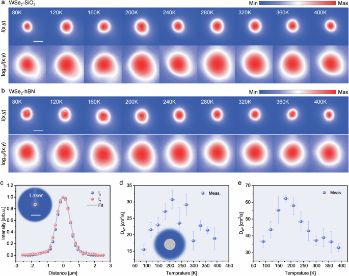
Spatial profiles of diffusion dynamics for exciton in WSe2-SiO2 (a) and WSe2-hBN (b). c Spatial intensity profiles of an excitation laser beam. Inset: micrograph of focused laser beam. Scale bar in (a)–(c): 2 μm. Temperature-dependent effective diffusion coefficients for exciton in WSe2-SiO2 (d) and WSe2-hBN (e).
Despite the high electron mobility of the TMDCs monolayer, the exciton diffusion length is typically only ~µm due to the short exciton lifetime66. Theoretical profiles of exciton emission (see Supplementary Note 7 for more details) can be derived for various effective diffusion coefficients Deff according to the exciton diffusion equation. To extract temperature-dependent exciton diffusion coefficient sensitively, the periphery of PL profiles (Blue region in Fig. 5d) away from the excitation center were integrated to monitor the subtle change in spot size due to the different exciton diffusion coefficients, learning from the commonly used eclipsing Z-scan method in nonlinear optics67,68. Comparing with the simulation results of exciton diffusion dynamics based on diffusion decay model, the temperature‑dependent effective diffusion coefficients Deff of excitons for both WSe2-SiO2 and WSe2-hBN can be estimated (See Supplementary Note 7 for more details). As shown in Fig. 5d, e, the non-monotonic temperature dependence of Deff can be observed in both WSe2-SiO2 and WSe2-hBN for the temperature ranging from 80 K to 400 K. However, owing to the encapsulation with hBN, the optimized temperature for Deff significantly decreases from 250 K to 200 K, as well as the Deff is enhanced by more than 100%, demonstrating a considerable dielectric encapsulation effect on exciton dynamics. Such different non-monotonous temperature-dependent behavior of Deff (Fig. 5d, e) demonstrate a remarkably consistent with the exciton emission efficiency (Figs. 3c, d), corroborating the above physical scenario of temperature-dependent excitonic emission efficiency.
Similarly, the non-monotonic temperature-dependent behavior of the Deff can be also reasonably explained by the competition between exciton localization in the potential disorder and phonon scattering40. At cryogenic temperatures, the scale of potential disorder is much larger than the thermal fluctuation kBT, thereby the exciton localization in potential disorder dominates exciton diffusion dynamics: Deff decreases as the temperature drops. When the thermal fluctuation kBT is increased to support the exciton escape from disordered potential well, the phonons scattering dominates exciton diffusion and brings about the exciton quenching: Deff and exciton emission efficiency decrease as the temperature rises. Therefore, the effects of potential disorder and phonons scattering create a dilemma for optimizing exciton diffusion dynamics and the optimized temperature is determined by the scale of potential disorder. The successful encapsulation with expected interlayer contact can leads to the adsorbates accumulating between the hBN and TMDCs layers, forming hydrophobic pockets and uniform regions, effectively reducing dielectric disorder and the induced potential disorder8. Consequently, the reduced potential disorder lead to a critical temperature corresponding to excitons escaping due to the hBN encapsulation, thereby the exciton diffusion has a lower optimized temperature with a weaker phonon scattering in WSe2-hBN, as well as the Deff has almost doubled69.
Discussion
The systematic investigation clarified excitonic transport and emission dynamics with managed potential disorder and phonon scattering in encapsulated atomically thin semiconductors. Compared with intrinsic monolayers, the WSe2-hBN demonstrates the modulated band structure and phonon vibration due to dielectric screening, as evidenced by PL and Raman emission measurements. The excitonic radiative lifetimes can be considerably shortened and exciton-exciton annihilation for the encapsulated monolayer can occur more quickly due to the increased Bohr radius and decreased binding energy of the exciton resulting from improved dielectric screening. The temperature-dependent excitonic spectral emission, particularly the excitonic linewidth and species, is significantly altered from the perspective of lattice dynamics. Additionally, the hBN encapsulation resulted in a significant optimization of the effective diffusion coefficient, with the optimal temperature decreasing from 250 K to 200 K and nearly doubled Deff, suggesting the reduced optimal temperature for exciton transport and emission by hBN encapsulation. These results can deepen our understanding the dielectric disorder and phonon scattering modulated exciton dynamics, paving the way for molding exciton flux and developing high-performance excitonic devices.
Methods
Sample fabrication
The sample was prepared by a dry transfer process following mechanical exfoliation. The hBN sheets were first exfoliated from massive crystals onto a polydimethylsiloxane (PDMS) substrate, and then thin layers were transferred to the SiO2/Si substrate. Through the same exfoliation process, the WSe2 monolayer was obtained, moved to hBN thin layers, and finally covered with hBN thin layers. The aforementioned samples were then subjected to a 30-minute duration at 300 °C in a nitrogen environment, followed by a cooling rate of 30 °C per minute down to room temperature to complete the annealing process.
Confocal Raman and PL spectrum measurements
PL mappings were performed by a confocal micro-Raman spectrometer (Horiba XploRA PLUS), employing an excitation laser with a wavelength of 633 nm. The Raman spectra were detected with a 100× objective lens (Olympus MPlan N, NA = 0.9) and 1800 mm−1 grating for the high spatial and spectral resolution (~1.8 cm−1). While for the PL spectrum, 600 mm−1 grating was used for high intensity. The step size of the PL image was set as 0.6 μm × 0.6 μm.
Fluorescence lifetime measurements
The fluorescence lifetime was collected by the FastFLIM system. The excitation source is a pulsed laser with wavelength 405 nm and frequency 40 MHz. The PL signals pass through a 480 nm long-pass edge filter and are finally collected by Nikon TE2000 microscope with a 60× NA = 1.2 WI objective lens.
Ultrafast measurements
Ultrafast pump-probe measurements in refection configuration were carried out. The femtosecond pulses (817 nm, 73 fs, 80 MHz) were split into two parts. One of them passed through a BBO crystal to produce the 405 nm pump pulses, while the other one was focused into a photonic crystal fiber (Newport SCG-800) to generate the super-continuum white light. The probe pulses were then selected with a 750 ± 10 nm (Thorlabs FB750-10) bandpass filter. The spot size of the focused probe and pump laser was <1 μm. The delay time between pump and probe pulses was controlled by a steeper linear stage (Newport M-ILS150PP). To improve the signal-to-noise ratio, the reflected probe pulses passed through a 650 nm longpass edge filter (Thorlabs FEL0450) and then were detected by a high-sensitivity photomultiplier (Thorlabs PMM02) connected with the phase lock-in amplifier (Stanford SR830).
Micro PL imaging
The schematic of micro PL imaging apparatus was presented in Supplementary Note 8. The femtosecond pulses (800 nm, 100 fs, 80 MHz) emitted from mode-locked oscillator (Coherent, Mira 900) were focused onto a BBO crystal to produce the 400 nm pump pulses. The second harmonic pulses passed through three shortpass filter (Thorlabs, FESH0700) to completely remove the fundamental frequency pulses and then tightly focused by an infinity-corrected long work distance micro-objective (Mitutoyo, 100×) to excite the WSe2 flakes. To record the diffusion dynamics of the excitons in monolayer, the 500 nm long-pass edge filter (Thorlabs, FELH0500) was used to block excitation light, the filtered light was imaged by an EMCCD (Andor, Newton DU971P). For spectral measurements, the filtered light was coupled to a spectrometer (Andor, KYMERA-328i-A, spectral resolution is 0.4 nm, phonon energy resolution is about 0.8 meV for 750 nm) equipped with an EMCCD (Andor, Newton DU971P). The home-made apparatus is convenient for switching between spectral measurement and spatial imaging by the removable right-angle silver mirror in cage cube.


Responses