Revealing stacking order transition via nanomechanical resonator

Introduction
Stacking orders in 2D layered materials refer to the arrangement of individual layers relative to neighboring layers. These arrangements can affect the interlayer coupling and the crystal symmetry, significantly modifying material properties and generating novel properties1,2,3. For instance, stacking orders in bilayer graphene influence the low-energy electronic band structures and induce new quantum orders such as superconducting and topological phases4,5. Stacking orders also control the vertical mirror symmetry in transition metal dichalcogenides, leading to the discovery of sliding ferroelectricity2,6,7,8. Meanwhile, weak vdW interactions between the adjacent layers make stacking order transitions much easier to manipulate than other covalent or ionic bond-breaking processes by reducing the energy barrier to the level of meV, which is promising for developing multistate and energy-efficient devices1,9.
Current methods for studying stacking order transitions mainly depend on electronic and optical responses. For example, optical responses such as Raman and Second harmonic generation (SHG) spectroscopies can show intralayer phonon modes or nonlinear susceptibility changes for various stacking orders only when certain symmetry requirements are satisfied to allow Raman-active or SHG active responses3,10,11. As for electrical detection, large electrical contrast can be observed only when strongly correlated states form in stacking orders at cryogenic temperatures5. To overcome the aforementioned limitations, a more universal detection approach is needed to probe a physical property that commonly exists in any stacking order transition without the presence of specific crystal symmetry and strong electron correlation. Indeed, mechanical properties, such as built-in strain are believed to change upon stacking order transitions12 due to the subtle unit cell variation. Although such strain change is universally applicable, probing it can be challenging. Considering the small unit cell’s difference during the stacking transition, the associated strain change is estimated to be on the order of 0.01%, which is beyond the capability of conventional strain measurements on 2D materials. To enable a mechanical detection approach universally applied for any stacking order transition, a new method is needed that is sensitive to subtle strain change.
In this work, we demonstrate a highly sensitive technique using circular nanomechanical resonators to reveal the strain change during the stacking order transition in thin membranes of octahedral MoTe2. Thanks to the high-quality mechanical cavity, we find a significant shift of the resonator frequency associated with the subtle strain change as the material transitions between the 1 T’ and Td stacking orders. The strain difference between the stacking orders is observed at the level of 10−4, which is one to two orders smaller than intralayer phase transitions in 2D materials13. Furthermore, we investigate how the resonance modes during the stacking phase transition are affected by critical parameters, such as high-order modes, electrostatic energy, and initial strain. Given its minimal constraints on crystal symmetry and conductance, this method holds potential for uncovering and exploring intricate stacking phase diagrams in various 2D materials.
Nanomechanical resonator based on MoTe2 membranes
We first design and fabricate circular mechanical resonators using 1 T’ MoTe2 membranes. MoTe2 is chosen because it exhibits two distinct stacking orders: a distorted octahedral (1 T’) phase and an orthorhombic (Td) phase (as shown in Fig. 1a. They share the same intralayer atomic structure, but the stacking orders differ, primarily induced by layer-to-layer sliding. The β angle of the 1 T’ phase and Td phase are 93°55’ and 90°, respectively14,15. Since the energy barrier between the two stacking orders is only a few meV per unit cell, the phase transition can easily be controlled by external stimuli, such as temperature16. Therefore, it provides a good platform for exploring stacking order transitions coupled with nanomechanical resonators. To create the nanomechanical resonator, thin MoTe2 flakes are mechanically exfoliated onto polydimethylsiloxane (PDMS) and subsequently transferred to prefabricated circular cavities, with diameters of 6 µm and depths of 600 nm (see in Fig. 1b). The cavities are connected by a 2 μm-wide venting channel to avoid flake damage during the vacuum pumping process. An optical image of one of the resonators with a MoTe2 membrane transferred on top is shown in Fig. 1b.

a Schematics of crystalline structures of 1 T’, and Td-MoTe2. The β angle of 1 T’ phase and Td phase are 93°55’ and 90°, respectively. b 2D nanomechanical resonator illustration (circular drum). Inset: an optical image of the device, the scale bar is 6 µm. c Calculated resonance frequency relation with MoTe2 thickness under varying tension: from the “membrane” limit to the “plate” region. With the strain change associated with stacking order transition, a clear frequency shift will be seen in the membrane region, while in the plate region, the difference is negligible. d Vibration amplitude of a few-layer MoTe2 resonator versus driving frequency. The ratio ({f}_{1}/{f}_{0}) between the second mode frequency and the fundamental mode frequency verified in the sample is in the membrane region. Note the amplitude of ({f}_{1}) has been magnified six times.
The resonance frequency in a MoTe2 nanomechanical resonator is given by
where (rho ,a,{mu }_{m},{rm{gamma }}) represent areal mass density, radius of the cavity, mode-dependent parameter and surface tension, respectively17,18. The bending rigidity (D) varies as the thickness of the flake changes by (D(t)={E}_{y}{t}^{3}/[12(1-{nu }^{2})]) (ν being Poisson ratio, ({E}_{y}) being the Young’s modulus and (t) being the thickness, see methods for more details). Based on this model, the relation between the resonance frequency of the fundamental mode and the thickness of MoTe2 flakes is shown in Fig. 1c, with different curves representing various tensions γ (0.1 N/m, 0.2 N/m, and 0.3 N/m). Here, 0.1 N/m corresponds to about 0.01% strain in a 10 nm membrane, the same level of strain possibly induced by the stacking transition from 1 T’ to Td phases. When the nanomechanical resonator is in the membrane region (Fig. 1c), especially when the thickness of the flake is small, where (frac{{rm{gamma }}{a}^{2}}{D(t)}to infty), the frequency is given by
and small changes to the surface tension will significantly impact the frequency. Conversely, with increased thickness, where (frac{{rm{gamma }}{a}^{2}}{D(t)}to 0), the tension dependence of the resonance frequency becomes negligible, and the nanomechanical resonator moves to the plate region. Therefore, the membrane region is employed here to explore the strain change during the stacking order transition in our experiments.
Strain changes in stacking order transition detected by nanomechanical response
With the fabricated MoTe2 nanomechanical resonator devices, we experimentally characterize the nanomechanical resonances during the stacking order transition via the laser interferometry technique (Supplementary Fig. 1 and methods) in a cryostat with temperature down to 1.7 K. To confirm the device vibrates in the membrane region and is potentially sensitive to small strain induced from the stacking transition, the ratio between fundamental mode frequency (({f}_{0})) and second-mode frequency (({f}_{1})) is analyzed in devices. In a typical mechanical resonance spectrum of a MoTe2 membrane (t = 12.6 nm) (Fig. 1d), both the fundamental mode frequency (({f}_{0})) at 7.052 MHz and the second mode frequency (({f}_{1})) at 10.075 MHz are observed in a MoTe2 resonator (t = 12.6 nm), giving a ({f}_{1}/{f}_{0}) ratio of 1.43. The result confirms the mechanical resonator is working in the membrane model with the expected ratio (~1.59), in contrast to the ratio ~2.03 in a plate model18. The slight difference of the ({f}_{1}/{f}_{0}) ratio between experiment and theory is caused by nonuniform initial strain induced by the fabrication process19. Moreover, atomic force microscopy (AFM) is performed to extract the pretension, Young’s modulus and thickness. The calculated frequency by membrane model matches well with experiment results and the contribution of plate model to the resonance frequency is negligible (details shown in Supplementary Note 2 and Supplementary Fig. 2).
To reveal how the nanomechanical resonator responds during the stacking order transition between 1 T’ and Td phases of MoTe2, the mechanical resonance at different phases are compared. To achieve different stacking orders in the same resonator, the phase transition in the MoTe2 membranes is induced by temperature change from room temperature (RT) to 1.7 K. Stacking orders are first identified by temperature-dependent resistance, similar to other reports20,21,22. As an evidence of first-order stacking transition, a clear hysteresis window between 70 K and 270 K is observed upon sweeping a loop of the temperature, where the middle point of the upper branch (point A at 170 K, cooling from room temperature) is dominated by the 1 T’ phase and the middle point of the lower branch at the same temperature (point B at 170 K, warming up from 1.7 K) is dominated by the Td phase.
With the control of stacking orders in MoTe2 through temperature, it is possible to test the mechanical response for each phase, and the hysteresis window provides access to each phase at the same temperature. Firstly, the resonance frequency of the fundamental modes for the 1 T’ phase at point A and the Td phase at point B (both at 170 K) of device #1 (t = 8.4 nm) are measured. In Fig. 2b, a clear frequency shift of 1.019 MHz from 14.090 MHz in the 1 T’ phase to 15.109 MHz in the Td phase is observed, along with a full width at half-maximum (FWHM) of 0.0063 MHz and 0.0056 MHz, respectively. By fitting the frequency to Eq. (2), the overall strain difference induced by the stacking order transition from Td to 1 T’ phase in the membrane is calculated to be 0.014%, where the Td phase shows larger strain and higher resonating frequency since it has the smaller volume of the unit cell considering the full-clamped boundary. The observed strain change is similar to other stacking order transitions reported by scanning transmission electron microscopy23. Considering the high-quality factor and the bandwidth, our resonator method gives a strain resolution of around 1.082 ppm, which is two orders higher than 232 ppm in conventional Raman spectroscopy (Supplementary Note 2). The frequency comparison between these two phases is done at the same temperature, hence it excludes the contribution of thermal expansion to the frequency shift24. And the frequency shift can be repeatedly observed during multiple temperature cycles (see in Supplementary Note 4 and Supplementary Fig. 3). Moreover, a temperature-dependent resonance frequency curve shows a clear hysteresis loop between 100 K and 250 K as well, verifying that structural transition happens in the membrane (Fig. 2c). The continuous frequency decrease is caused by thermal expansion as the temperature increases17,25.
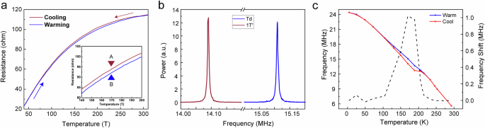
a Temperature-dependent resistance. Hysteresis between cooling (from RT) and warming (from 1.7 K) (in red and blue curves respectively) corresponds to the 1 T’-Td phase transition. The middle of the hysteresis region is marked by black and red arrows, points A and B, dominated by 1 T’ and Td phases, respectively. bThe fundamental mode frequencies for 1 T’ phase at point A and Td phase at point B. Significant changes in resonance frequency (1.019 MHz, 7.24% shift) are observed along with a high-quality factor (>2000) based on (device #1, t = 8.4 nm). c hysteresis of fundamental resonance frequency of the MoTe2 resonator and the dash line shows the frequency shift between the cooling and warming process.
Taken together, the above results demonstrate the feasibility and high sensitivity of our new approach to detect stacking order transition based on mechanical property change. To understand the impact of extrinsic stimuli and intrinsic resonance modes on the detection capability and further improve the sensitivity, we conducted the following systematic studies.
Electrical modulation and strain-controlled resonance change in 1 T’-Td stacking order transition
The resonant frequencies of the stacking orders can be controlled by electrostatic gating, which induces capacitive softening and electrostatic stiffening to the membrane26,27,28. This can impact on the frequency difference between the phases, and thus the sensitivity of our detection of the stacking order. To explore these changes, we measure how the fundamental modes for both 1 T’ and Td phases of device #2 (t = 12.6 nm) shift as the gate voltage between the Si and MoTe2 flake (Vg) varies (Fig. 3a). The peak amplitude of the resonance increases with Vg since the driving force becomes larger29. Next, the gate-dependent resonance frequencies for each phase are summarized in Fig. 3b. The 1 T’ phase and Td phase are measured at the same temperature (170 K) for all gate voltages. Both phases exhibit similar trends, where the frequency decreases upon increasing Vg below 35 V and begins to increase when Vg is sufficiently large (>35 V) and can be fitted by (details in Supplementary Note 5):
where (alpha =frac{4.9{E}_{y}t}{{(2pi )}^{2}{M}_{eff}},,beta =-frac{{in }_{0}pi {R}^{2}}{{(2pi )}^{2}{M}_{eff}3{g}^{3}},,varGamma =frac{pi {in }_{0}^{2}{R}^{2}}{{(2pi )}^{2}{M}_{eff}8(1-{v}^{2}){E}_{y}t{varepsilon }_{0}{g}^{4}}) (ϵ0 being the vacuum permittivity, g being the cavity depth, Ɛ0 being the initial strain). From left to right, the terms in Eq. (3) refer to elastic energy arising from initial strain, electrostatic energy from capacitance, and elastic energy from elongation effect30. By fitting the frequency versus gate curves to Eq. (3), we extract α, β and Γ for both phases. More interestingly, by subtracting the two curves in Fig. 3b, the resonance shift (({varDelta f}_{0})) between the two stacking orders shows two regions of gate dependence. When Vg < 35 V, the frequency shift is almost independent of the gate voltage. In contrast, when Vg > 35 V, the frequency shift begins to decrease as the voltage increases. This observation can be explained by the model derived from (3)
where ({alpha }_{{Td}}{varepsilon }_{{0}_{{Td}}}-{alpha }_{{1T}^{{prime} }}{varepsilon }_{{0}_{{1T}^{{prime} }}}, >, 0,{Gamma }_{{Td}}-{Gamma }_{{1T}^{{prime} }}, <, 0) and ({beta }_{{Td}}-{beta }_{{1T}^{{prime} }}approx 0). In equation (4), only the second term, from the stiffening effect, shows a strong gate dependence in the sufficiently high voltage region as the parameter ({alpha varepsilon }_{0}) is orders larger than the (varGamma) parameter, which leads to the frequency shift decreasing. While in the scenario with no additional electrostatic gating, the first term (({alpha varepsilon }_{0})) dominates in the frequency shift during stacking order changes, where the initial strain (({varepsilon }_{{0}_{1{T}^{{prime} }}})) in the flake is introduced during the transfer process31,32,33. The change of fundamental frequency follows ({varDelta f}_{0}propto frac{1}{sqrt{{{rm{gamma }}}_{0}}}varDelta {rm{gamma }}), based on Eq. (2) considering the same tension change (Δ({rm{gamma }})) during the stacking order transition, equivalently the strain change linked by (varDelta varepsilon =varDelta {rm{gamma }}/{E}_{y}t), which points out that with lower initial strain ({varepsilon }_{0}) (initial tension ({{rm{gamma }}}_{0})) in the flakes, the resonance frequency is more sensitive to the strain change induced by the stacking order change. Figure 3d summarizes the fundamental frequency and its relationship with the tension. When we select the same tension change ((varDelta gamma )) (such as 0.125 N/m, which corresponds to the tension shift induced by sliding in experiments), the shift (varDelta f) increases as the initial tension (({{rm{gamma }}}_{0})) decreases. We summarize the resonance shift on multiple devices with various initial strains (shown in Fig. 3e) and find it is consistent with the predicted trend. The measured resonance responses of devices are detailed in Supplementary Note 6 and Supplementary Fig. 4. Among them, with the minimal initial strain 0.12%, a notable frequency shift of 0.96 MHz of the fundamental resonance mode is observed. Thus, we show that the resonance frequency for different stacking orders can not only be tuned by the electrostatic modulation but also influenced by the initial strain.
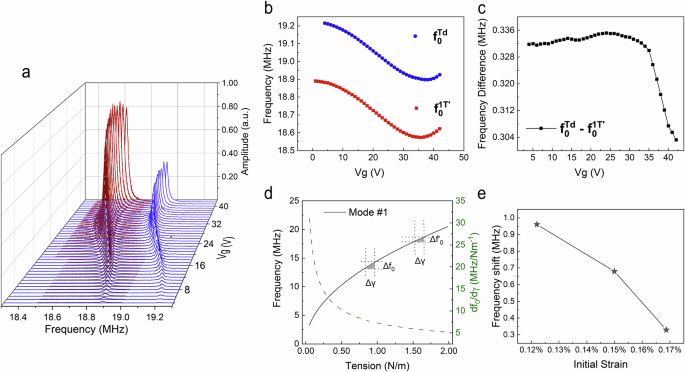
a Gate-dependence of the fundamental mode resonance vibration of device #2 (t = 12.6 nm) under different phases. The red curve represents the 1 T’ phase and the blue curve represents the Td phase. b The gate-dependent fundamental resonance frequency ({f}_{0}) for each phase. c The gate-dependent frequency difference between 1 T’ and Td phases. At the low voltage region, the frequency difference is almost independent of the gate voltage, while at high voltage region, the frequency difference begins to decrease. d The modeling of initial tension-dependent fundamental frequency ({f}_{0}) (solid line) and first-order derivative of ({f}_{0}) (dash line) for an ideal MoTe2 membrane based on Eq. (2). When we choose the same tension change (varDelta gamma) (such as 0.125 N/m, which is the same level to sliding induced tension shift in experiments), the shift (varDelta f) increases as the initial tension decreases. e The frequency shift of measured devices relates with their initial strain. The devices with smaller initial strains show more frequency shift during the stacking order transition.
Higher order mechanical modes responses to stacking orders change
With the substantial quality factor which allows access to higher-order mechanical modes, we also reveal how they can yield larger responses to the stacking order transition. Figure 4a shows the measured frequencies of the first two modes of device #3 (t = 10.5 nm). The fundamental mode frequency shifts from 17.27 MHz in the 1 T’ phase to 17.60 MHz in the Td phase, resulting in a 0.33 MHz shift, whereas the second mode frequency changes from 24.24 MHz to 25.08 MHz, leading to a much larger shift of 0.84 MHz. This result shows that the frequency shift becomes larger in the higher modes. To establish the relationship between the modes and stacking order transition, we performed finite element modeling (FEM) simulations, using COMSOL, to calculate the multiple higher eigenmodes (Fig. 4b), in which a fully clamped circular membrane (d = 6 µm, t = 10.5 nm, depth = 600 nm) model with a trench (width being 2 µm, depth being 600 nm) has been built and assigned with real materials properties (see “Methods” for details). The ratios of the frequency shifts of the higher modes (Modes #2,3,4) to that of the fundamental mode (Mode #1) are 1.60, 2.09, and 2.69. These agree well with the theoretical ratios of μm/μ0 which are 1.59, 2.13, and 2.6534, respectively. Both experimental results and simulation can be understood by the frequency shift ({varDelta f}_{m}propto {mu }_{m}varDelta sqrt{{rm{gamma }}}), with the same tension change ((varDelta sqrt{{rm{gamma }}})), where the frequency shift is proportional to the eigenvalue ({mu }_{m}) for each mode34. It is also repeated in device #2 (see Supplementary Note 7 and Supplementary Fig. 5), which shows that the Δf2/Δf0 is 2.012, aligning well with the ratio of µ2/µ0 = 2.13. This confirms that the resonance frequencies of the higher order modes, which are accessible for high-quality mechanical resonators, can show a larger frequency shift during the stacking phase transition and therefore provide higher resolution for phase identification.
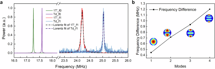
a Vibration of the fundamental mode (Mode #1) and the higher mode during stacking order transition measured at 170 K for device #3 (t = 10.5 nm). The frequency shifts are 0.33 MHz and 0.84 MHz, respectively. b COMSOL model for the frequency shift for multiple vibration modes during the stacking order transition.
In conclusion, we have demonstrated a sensitive method for detecting strain change in stacking order phase transitions based on nanomechanical resonators. The induced strain change at the level of ppm during the stacking transition can be reflected by the resonance frequency. Our study of the multimode resonance frequencies under different phases shows that the frequency shift induced by the strain is increased in higher modes and the resonance frequencies shift demonstrates tunability in response to gate voltage and initial strain. Moreover, this technique is adaptable to other stimuli, such as magnetic fields35, strain36, and electric fields37, making it a versatile platform for studying emergent stacking transitions, such as sliding ferroelectricity and stacking magnetic orders. Overall, this method provides a new and general opportunity for uncovering the rich stacking order phase diagram and their resulting physics in van der Waals materials without restriction on symmetry.
Methods
Sample fabrication
Circular cavities were fabricated by reactive ion etching to generate holes of 6 µm in diameter on a Si wafer with 290 nm of SiO2 on top. A circular cavity is also etched in the same step, connecting with a 2 µm venting channel to prevent the membrane from breaking during the venting and pumping process. Flakes of 1 T’-MoTe2 are exfoliated on the PDMS from high-quality bulk single crystals grown by a self-flux method38. Following the exfoliation, flakes are transferred on the pre-patterned chip by an all-dry transfer method39. For conducting gate sweeping experiments, Ti/Au electrodes are initially patterned using typical photolithography and e-beam deposition techniques. The sample thickness was measured by a Cypher S AFM Microscope equipped with OMCLAC160TS-R3 Titan 300 AFM tips. Contact mode was employed to measure the sample thickness, while single force mode was utilized to obtain the force spectroscopy data.
Measurement setup
The sample is mounted inside an optical cryostat (Quantum Design, OptiCool) and can be precisely positioned using a piezoelectric stage. The vibration of the nanodrum is actuated by a weak RF signal of ~100 mV generated by a VNA (Agilent E5062A). Membrane displacement is then measured interferometrically with a He–Ne laser (λ = 632.8 nm), whose reflection is modulated by the optical cavity formed between the vibrating membrane and Si substrate40. The optical signal is then reflected to an ultrafast photodetector (APD430A, Thorlabs), and analyzed by the same VNA. The amplitude of vibration is maximized when the driving frequency is equal to the resonance frequency, which corresponds to a peak in the S21 curve. The power of the incident laser is set below 3 µW to minimize heating effects on frequency (see Supplementary Note 8 and Supplementary Fig. 6) and the spot size is 1 µm. The temperature-dependent transport measurements were measured by four probe methods.
Modeling for mechanical cavity
The Structural Mechanics Module in COMSOL Multiphysics 6.0 is used for the finite element modeling (FEM) simulations. The 2D material is modeled as a circular membrane with a diameter (d) of 6 µm and a thickness t of 10.5 nm. The boundary of the membrane is fixed except the venting trench (width of 2 µm, oriented along y direction, shown in Fig. 1b). Different mechanical properties are assigned for different phases of MoTe2 (density of 7700 kg/m3, Young’s module of 99 GPa and Poisson Ratio of 0.42 for 1 T’ density of 7700 kg/m3, Young’s module of 102 Gpa and Poisson Ratio of 0.19 for Td41). Anisotropic in-plane forces (({gamma }_{x},)= 2.118 N/m and ({gamma }_{y}) = 1.156 N/m for 1 T; ({gamma }_{x},)= 2.207 N/m and ({gamma }_{y}) = 1.25 N/m for Td) are added to the membrane to model the nonuniform initial strain and make the frequency of the first two modes consistent with the experiment results.


Responses