Solution-processable 2D materials for monolithic 3D memory-sensing-computing platforms: opportunities and challenges

Introduction
Silicon CMOS microchip has been the cornerstone of microelectronics for several decades, enabling remarkable progress in computing and memory technology. In the past decades, the ongoing trend of scaling down device dimensions has significantly propelled advances in key metrics (power, performance, area and cost reduction) of silicon technology1. These advancements have led to various technological revolutions, including the rise of Artificial Intelligence, the Internet of Things and Big Data, and thus have brought forth new demands for data collection (sensors), processing (computing unit), and storage (memory) in the future energy-efficient and data-centric electronic system. However, silicon-based CMOS devices are encountering insurmountable challenges due to limitations in miniaturization and escalating complexities in manufacturing processes. The traditional separation of memory and logic units in the von Neumann computing paradigm has also created bottlenecks in energy efficiency, prompting a shift towards in-memory and near-memory computing models2,3. In addition, with the exponential growth of sensory nodes4, it becomes imperative to not only explore cost-effective and practical methods for integrating new materials on silicon CMOS wafers, but also to innovate novel mechanisms and architectures capable of efficiently processing unstructured and redundant sensory data within this evolving computing paradigm.
In this context, M3D integration, as illustrated in Fig. 1, where sensors, memories, and transistors are incorporated sequentially above silicon CMOS logic between layers of fine-grained and dense vertical interconnects, holds significant potential as a key enabler for system-on-chip hyperscaling5,6. By stacking and connecting the memory, computing, and sensor units closer through dense vertical interconnections (vias), the data communication bandwidth is greatly improved, and thus latencies associated with data exchange bottleneck between compute and memory can be substantially reduced, enabling efficient on-chip data-abundant processing. Despite the promising nature of such 3D systems, there are fundamental obstacles that must be overcome. One major roadblock is the incompatibility between the thermal budget of the transistors and interconnects. Advanced low resistivity copper interconnects with low-(kappa) dielectric interlayers are unable to withstand thermal exposure above 400 °C. However, the thermal activation of dopants in silicon-based devices typically occurs between 600 and 1000 °C. Therefore, processing silicon transistors below such temperatures results in performance and reliability degradations.

An overall graphic illustration of M3D integration of memory, sensing, and computing devices with solution processable 2D materials. This provides a comprehensive visual representation of the key components and concepts central to the discussion in this review.
The current dilemmas with silicon material for massive 3D systems have motivated persistent efforts in the search for beyond silicon materials solution. Among them, 2DMs, a broad class of nanomaterials, offer a myriad of opportunities to tailor the electronic properties with desired mobility, bandgap, and carrier concentration, essential for the realization of highly efficient M3D circuits5,7,8,9. On one hand, the atomically thin nature of 2DMs can help mitigate short-channel effects, such as drain-induced barrier lowering (DIBL), which is crucial for scaling transistors below 3 nm technology nodes10. On the other hand, 2DMs can be integrated with low-thermal budget processing, making it a compelling technology for M3D integration compatible with thermal process constrained interconnects (e.g. low-(kappa) dielectric and copper interconnects). Furthermore, 2DMs encompass a wide variety of electronic building blocks ranging from semiconductors11,12,13, insulators14,15,16, ferroelectrics17,18,19,20, magnets21,22,23, to topological insulators24,25,26. This diverse range of properties and functionalities provided by 2DMs offer flexible designs of innovative memory, sensing and computing devices and a unique platform for the rapid design and implementation/verification of M3D circuits. Moreover, the weak van der Waals (vdW) interlayer bonding, diverse electronic properties and wide range of vacancy dynamics associated with 2DMs and vdW heterostructures offer a new palette to engineer their defects, composition, and even stacking sequences for monolithic integration of devices with different functionalities, such as storage, computation, and sensing, on a single chip27. Especially, the high surface-to-volume ratio and versatile functionalization make 2DMs well-suited for gas, chemical, and biosensing applications. Therefore, the fusion of various 2DMs functional devices through M3D integration can lead to compact and multifunctional integrated circuits with enhanced system performance and area efficiency beyond the conventional von Neumann architecture.
So far, deposition and transfer of 2DMs are active areas of research and development, with promising progress28,29,30. However, they have not yet reached full manufacturability and the current approaches to wafer-level, defect-free, single-crystalline growth and transfer still present fundamental challenges. As such, the feasibility of such approaches for seamless integration with silicon CMOS technology and final translation into future M3D circuits is still in question. Such co-integration technology has to overcome hurdles from key ‘unit process’ for wafer-level scalability, reliable high-throughput thin-film transfer processes and CMOS-compatible integration techniques31. In contrast, solution-processable 2DMs not limited by wafer-scale transfer process, offer an interim and alternate integration option. Solution-processable 2DMs refer to a distinct class of 2D nanosheets that exhibit the ability to disperse in various solvents, allowing for facile processing and manipulation like organic materials32. The solution processability of these 2DMs nanosheets enables them to be deposited onto various substrates or the fabrication of thin films through scalable and cost-effective liquid-based techniques such as spin-coating33,34, drop-casting35, printing36,37,38, self-assembling39,40,41, etc. Despite their solution-based processability, they retain the excellent electronic performance and structural stability of crystalline inorganic materials, making them attractive for a wide range of applications in electronics, optoelectronics, energy storage and sensing5,32,33,42,43,44,45,46,47. Furthermore, with low process temperature and compatibility with high-precision optical lithography patterning, solution-processed 2DMs offer a practical approach for the M3D integration of tall and flexible 2DMs stacking that circumvents the challenges faced by chemical vapor deposition (CVD) synthesis and mechanical transfer process.
In view of the many advantages that solution-processable 2DMs bring for the next generation of monolithic 3D electronics, we aim to present a comprehensive review that covers recent advances, open challenges and future perspectives of solution-processable 2DMs-based devices, ultimately steering towards the convergence of memory, sensing, and computing functionalities. The overview of this review is encapsulated in Fig. 1, highlighting four key aspects. First, from the perspective of material science, we review the past decade of progress in exfoliation chemistry, deposition techniques and post-processing treatments. This initial section elucidates how various advancements in this domain enabled the development of electronic grade 2D nanosheets and films for different devices applications. Building upon this foundation, we transition seamlessly into device applications. This section explores the performance limitations and breakthroughs of solution-processable 2DM-based transistors, memristors and photodetectors. To optimize device performance for future sensing-memory-computing systems, the third section offers a detailed review of the fundamental charge transport mechanisms in solution-processed 2DMs devices. Additionally, we delve into the critical process parameters for the heterogeneous integration of 2DMs-based memory, sensing, and computing functionalities, as well as novel computing systems and architectures. Lastly, we summarize the challenges and potential synergies emerging from the logic-memory-sensing convergence, culminating in a comprehensive outlook that addresses the hurdles and prospects on the horizon for solution-processable 2DM-based electronics.
Materials synthesis and deposition
Exfoliation and formulation of 2D dispersions
The reliable generation of well-dispersed 2D nanosheets in a solution with long-term stability and nanosheet size/thickness homogeneity is essential for the subsequent assembly of thin films formed from a network of 2D nanosheets. These nanosheets need to exhibit a range of interesting flake-size dependent electronic properties to enable diverse nanomaterial functionalities as a thin film composite, including metallic (e.g., graphene48,49,50), semiconducting (e.g., transition metal dichalcogenides, TMDCs38,41,51 and black phosphorus, BP52,53,54), and insulating (e.g., hexagonal boron nitride, h-BN15,50,55) characteristics. Generally, there are two approaches to producing 2D nanosheet dispersions: the bottom-up synthesis34,56,57,58 and the top-down exfoliation strategies59,60. The former usually involves a highly specific colloidal chemistry process and undesired surface ligands, leading to 2D nanosheets with poorly controlled chemical composition, broad width/thickness distribution and compromised electrical properties (e.g. conductivity and mobility), thus rarely used for electronic purposes. Instead, top-down exfoliation approaches, which utilize either direct liquid-phase exfoliation (LPE) or intercalation-assisted exfoliation technique as shown in Fig. 2a-c, have demonstrated to be more effective for producing graphene61,62, h-BN54,55, 2D TMDCs63,64,65, BP66,67, etc. Because of their anisotropic bonding (covalent within the layer and van der Waals interactions between layers), external forces such as high-power sonication or high-shear mixing typically involved in the direct LPE process can be utilized to overcome the weak interlayer interactions in 2D bulk crystals and facilitate the isolation of mono- to few-layer nanosheets. Despite a straightforward and general approach, direct LPE usually suffers from long-term agitation, poor exfoliation yield ((< 40 %)) as well as small nanosheet size (<1 µm)44. Furthermore, the use of organic solvents with high-boiling points, such as N-methyl-2-pyrrolidone or dimethylformamide, introduces surface contamination68.

a Direct LPE. b Electrochemical exfoliation with the assist of large molecules intercalation. c Electrochemical exfoliation with the assist of small ions intercalation. Comparison of direct LPE and electrochemical exfoliation in terms of (d) thickness and lateral dimension of exfoliated nanosheets, and (e) exfoliation yield as a function of exfoliation duration. f Example of MoTe2 flake size distribution produced from intercalation with large molecules. Panel f reprinted with permission from ref. 238, American Chemical Society.
Recently, intercalation-assisted exfoliation technique (also called electrochemical exfoliation technique) has been developed to enhance the exfoliation yield by inserting either small-sized alkali metals or large-sized organic ammonium cations between the vdW interlayers prior to exfoliation63,64,65,67,69,70,71,72. The intercalation process increases interlayer spacing without breaking intra-layer covalent bonds, significantly weakening the interlayer bonding, thus facilitating the subsequent delamination steps. Compared to direct LPE, intercalation-assisted exfoliation allows the production of high-quality 2D nanosheets with significant improvement in average aspect ratio and less exfoliation duration (Fig. 2d, e)73. Intercalation with alkali metal ions like Li+ and Na+ has been demonstrated to be a viable method for selectively producing pure mono- or few-layer TMDC nanosheets. For instance, monolayer MoS2 nanosheets were achieved with a yield of 92%74, monolayer TaS2 nanosheets with a yield of 93%75 and bilayer TiS2 nanosheets with a yield of 93%76, all exhibiting lateral dimensions in the micrometer scale. However, the fast and spontaneous lithiation process can introduce many defects77 or cause semiconducting to metallic phase transition (e.g., semiconducting 2H to metallic 1 T/T’ phase transition in MoS2) due to the excessive injection of electrons78.
Replacing the small Li+ ions with large organic ammonium cations, such as quaternary ammonium ions, allows for a milder reaction and mitigated electron doping, resulting in few-layered semiconducting nanosheets with desired phase and minimum structural damage32,65,66. For example, phase-pure, semiconducting 2H-MoS2 nanosheets have been achieved by the insertion of organic quaternary ammonium molecules, which enables a tremendous increase in interlayer spacing of host MoS2 crystal from the original 6.1 Å to 22.9 Å65. Yu et al. optimized the electrochemical intercalation method with the assistance of polyvinylpyrrolidone, which enables the high-yield (>95%) exfoliation of micron-sized (5-10 µm), monolayer MoTe2 nanosheets (Fig. 2f). It is important to note that intercalation-assisted exfoliation is a complex process that depends on several factors, including the intercalant size and chemistry, interlayer spacing, inherent intralayer bond strength, intercalation conditions, etc. The effect of molecule size on the geometric dimensions of 2D nanosheets has been investigated by comparing the intercalation with tetrapropylammonium (TPA, molecule size d (approx) 10 Å) and tetraheptylammonium (THA, molecule size d (approx) 20 Å) in the exfoliation of ReS2 flakes, respectively63. A critical molecular size effect was found, where the larger-sized THA exhibited improved efficiency in producing thinner and bigger ReS2 nanosheets with an increased density of grain boundaries. However, there is a tradeoff between the intercalant size and diffusion kinetics. On one hand, the increase in the intercalant size causes dramatic interlayer expansion, which could weaken the interlayer bonding beneficial for the delamination of bulk crystals. On the other hand, it increases the intercalation barrier through a notorious self-retarding effect64, where the presence of large-size ammonium cations already intercalated within the vdW gaps creates significant elastic and electrostatic interlayer repulsions, preventing complete intercalation in every vdW gap79,80,81.
Several strategies have been reported to address the self-retarding issues or high diffusion barriers. A co-intercalation of organic ammonium cations solvated with neutral solvent molecules is reported as an efficient strategy for sufficient intercalation of bulk crystal and notably reduces the excessive charging and structural damage of the layered hosts36. With such strategy, a wide range of superconducting 2D monolayers (e.g. NbSe2, NbTe2, TaS2, TaSe2, TiS2, TiSe2 and MoTe2) have been produced with lateral dimensions up to 300 µm36. In addition, the self-refreshing process through intercalation-induced strain is another solution to self-retarding effect64. But such a strategy only applies to certain 2D materials with high rigidity such as In2Se382, InSe and Bi2Se364, which experience intense mechanical strain during intercalation, leading to a sequential process of bending, fracture, and detachment from the bulk crystals. As a result, underlying fresh surfaces are continually exposed for intercalation and thus effectively avoid the self-retarding effect.
Assembly and deposition of 2D film
The scalable assembly of liquid-exfoliated 2D nanosheets into continuous and large-area thin films represents a crucial step towards their implementation in solid-state electronic devices for memory, sensing, and computing applications. To this end, a plethora of techniques, such as spin coating33,34,65, inkjet printing49,50,83,84,85, aerosol jet printing38, Langmuir-Blodgett assembly41,86,87 and electrostatic deposition39, each with its distinct advantages and disadvantages, have been developed for the scalable assembly of composite thin film from solution-processed 2D nanosheets. The appropriate deposition technique should be selected to form the desired thin film structures based on the material’s properties and target applications. In this review, we will specifically delve into the most widely adopted methods, namely spin coating, inkjet printing, and Langmuir-Blodgett assembly (Fig. 3a-c). As a versatile technique, inkjet printing is a promising approach because of its precise control over the deposition process, high resolution (~50 µm) and low material losses ( < 1 mL)88. During the printing process, the droplets containing the 2D nanosheets dispersions are ejected from the micro-sized nozzles onto target substrate in a highly controlled and precise manner, creating complex patterns and intricate designs. Unlike traditional lithography techniques, inkjet printing enables on-demand deposition of 2D nanosheets onto any substrates in a maskless and non-contact deposition mode, thus suitable for large-scale, flexible and wearable electronics. Various electronics have been demonstrated by inkjet printing different 2D materials inks ranging from graphene89 to TMDCs37,51,90,91,92,93, BP53, etc. A comprehensive engineering of ink properties (e.g. surface tension, viscosity, boiling point, and concentration) must be performed to realize stable 2D inks and ensure satellite droplet-free ejection, high throughput, as well as uniformly printed films85.

Film deposition techniques for 2D dispersions and their corresponding nanosheets alignment morphology. a Printed film with oblique alignments. b Spin coated film with plane-to-plane alignment. c Langmuir-Blodgett assembled film with edge-to-edge alignment. Scalebars in b and c are 10 nm and 2 µm, respectively. Post processing treatment of the solution-processed film. d Chemical treatment. e Thermal annealing. f Laser thinning. Panel a reprinted with permission from ref. 33., Springer Nature Limited; Panel b reprinted from ref. 50., Springer Nature Limited; Panel c reprinted from ref. 40., American Chemical Society.
Despite their huge potential, the printed electronic devices reported to date are still challenged by poor performance and large device-to-device variation inferior to those made from exfoliated flakes or CVD film. This discrepancy comes from the morphology of the printed film, or more specifically, the alignment of the nanosheets. Figure 3a presents a scanning electron microscope image of the channel region from an inkjet-printed h-BN/graphene heterostructure transistor, where randomly aligned nanosheets with poor interface and pinholes are clearly seen in the vertical vdW stacks50. In such a system, charge transfer across the inter-sheet junction experiences high parasitic resistance that ultimately deteriorates their film mobility. As a result, the film mobility from the printed nanosheets generally falls within a narrow range between 0.01 ~ 1 cm2V−1s−1, almost two orders of magnitude lower than the mobility of mechanical exfoliated TMDCs (~50 cm2V−1s−1)90, MXenes (~100 cm2V−1s−1)94 and graphene nanosheets ( > 10,000 cm2V−1s−1)95, respectively. This highlights the fundamental role that inter-sheet junctions play in moderating the network properties, which will be illustrated in greater detail in Section “Physical insights into the charge transport mechanism in solution processable transistors, RRAM and sensors”. An intriguing exception to the reduced mobility has been reported for the MoS2 semiconducting film and Bi2Se3 conductive film produced by spin-coating. Remarkably high thin-film mobility of approximately 10 cm2V−1s−1 for MoS265 and 113 cm2V−1s−1 for Bi2Se334 are achieved, respectively, which are even comparable to their individual nanosheets. This exceptional performance can be attributed to the nanosheets’ inherent flexibility and reduced grain boundaries associated with thin and large nanosheet geometry, leading to a favorable large-area plane-to-plane alignment (Fig. 3b). Consequently, a significant reduction in junction resistance occurs, effectively shifting the rate-limiting factor to the intrinsic resistance of the nanosheets. Therefore, spin-coating has been widely employed for depositing 2D nanosheets onto different substrates, offering simplicity and capability for producing high-quality and uniform thin films. However, achieving full coverage on a substrate often demands high nanosheet concentration (e.g., 10 mg/mL) during spin-coating iterations65, which will not only cause substantial materials waste and stability concern of the 2D dispersions, but also impose challenges for precise control over film thickness and architecture, resulting in irregular structure of agglomerated nanosheets after the solvent evaporates.
Alternatively, given exceptional versatility and capability of microstructural control, the Langmuir–Blodgett (LB) assembly approach is becoming increasingly popular for the deposition of large-area thin film with superior 2D nanosheet alignment and uniform thickness (Fig. 3c)39,87,96,97,98. It offers precise control over nanosheet density and relative orientations within a monolayer, capable of fabricating well-defined thin film structures with customized number of layers. In a typical LB assembly procedure, the 2D nanosheets are initially dispersed in a volatile water-immiscible organic solvent, followed by spreading onto the water surface. After the spreading solvent evaporates, a monolayer consisting of 2DM flakes forms on the water, which is subsequently transferred to the target substrate, eventually creating a large area of flat 2D thin film. Through LB assembly at the air/liquid interface, monolayers of diverse colloidal 2DMs have been widely demonstrated so far39,40,87,98,99,100. However, there are some concerns associated with air/liquid confinement in LB assembly. One issue is the material loss to the water subphase during the transfer process, leading to the reduction in monolayer quality and yield. Furthermore, the compression of particles at the air/liquid interface may lead to aggregation, compromising the uniformity of the assembled monolayer. As a result, liquid/liquid confinement techniques have been further utilized to enhance the alignment of nanosheets86,98. The choice of solvents for interfacial confinement in LB assembly plays a crucial role in determining the film quality, structure, and functionality. Different solvents possess varying polarities, surface tensions, and viscosities, which in turn influence the assembly process and the packing of the molecules or nanoflakes in the resulting LB films. For example, a monolayer of ultrathin sheets of highly hydrophobic graphene nanosheets was assembled at the chloroform/water interface86. Driven by the minimization of interfacial energy, the graphene nanosheets spatially confined at the immiscible liquid/liquid interface produce a closely packed monolayer structure with excellent electrical conductivity (1000 S/cm) and optical transmission (>70% @ 550 nm). In the case of MoS2, the water/hexane system, characterized by its high interfacial tension (~50.5 mN/m), was deliberately selected to create the interface, leading to the self-assembled tiling of MoS2 bilayer nanosheets with edge-to-edge contacts between nanoflakes (Fig. 3c). Remarkably, over 70% of the film is covered by single flakes without overlapping, showcasing the efficacy of this solvent-driven approach in achieving highly organized and non-overlapping thin films. However, scaling up the LB assembly process to produce films over a wafer scale with consistent quality can be very challenging, which needs delicate control over the interfacial conditions and solvent interactions to promote the desired arrangement of the materials. Overall, maintaining a stable interface during the assembly process, achieving well-spread nanosheets with minimal aggregation at the interface, and ensuring a steady and controlled film transfer process are the three most important considerations for successful LB film fabrication.
Post treatment of 2D film
Low interface quality and abundant defect density or dangling bonds at the flake junction regions largely compromise the electronic properties of solution-processed 2D film due to the charge trapping of carriers. Therefore, enhancing the quality of nanosheet films and mitigating defects through post-treatments such as thermal annealing, chemical modifications (e.g. bis(trifluoromethane) sulfonimide101 or conjugated 1,4-benzenedithiol treatments) and laser thinning presents a promising pathway for high-performance electronics (Fig. 3d–f). These strategies hold significant potential for optimizing the electronic properties of nanosheet-based materials.
Thermal annealing stands out as the primary post-processing technique, widely employed to eliminate volatile components and polymeric additives within the nanosheet film. In some cases, certain polymers can promote nanosheet doping49,102, but their presence within a network typically creates physical barriers between nanosheets. The elimination of polymers brings about several benefits. Firstly, it triggers a collapse in the network structure89, leading to reduced porosity. This structural transformation facilitates closer contact between nanosheets. Furthermore, the resulting carbonization leaves behind a residue that might enhance inter-sheet charge transfer under specific conditions103. The conductivity of the nanosheets film is highly correlated to the annealing temperature. Annealing temperature higher than 250 °C is usually required to fully remove the polymer and maximize the conductivity. Besides, the annealing temperature may vary depending on the types of polymers. For instance, Secor et al. 104. systematically studied the electrical conductivity of graphene networks as a function of annealing conditions. They found that annealing at 250 °C for 20 minutes effectively removed the polymeric binder ethyl cellulose, achieving a maximum conductivity of 2.5 × 10⁴ S/m. In the case of polyvinylpyrrolidone, He et al. 105. reported that annealing between 300-350 °C is necessary to convert polyvinylpyrrolidone into a thin layer of amorphous carbon, resulting in π-π stacking that bridges graphene flakes. This significantly enhances the conductivity of the network, reaching 8.8 × 10⁴ S/m. However, it is important to note that the thermal stability of nanosheet materials can impose limitations on the annealing temperature. For instance, TMDCs, like WSe2 are very vulnerable to oxygen and moisture. Annealing those chalcogenides at temperatures exceeding 200 °C in an oxygen-rich environment can trigger undesired p-type doping106. Moreover, temperature beyond 300 °C might induce considerable oxidation, converting the material to oxides106,107. The thermal budget places constraints on annealing temperatures, necessitating the adoption of additional protective measures such as vacuum or inert gas environments. This is crucial to prevent degradation of material quality and enhance the conductivity of the networks.
Complementary to thermal annealing, chemical treatments serve as another valuable tool for enhancing the properties of solution-processable 2D nanosheet films (Fig. 3d). Generally, the energetic liquid exfoliation procedure often introduces abundant structural defects like chalcogen vacancies in TMDCs. Those defects, unfortunately, can hamper the potential of these materials, especially in applications related to optoelectronics. Moreover, certain 2D materials, such as BP, are intrinsically unstable during solution processing, posing limitations for their practical use under ambient conditions. In the face of these challenges, the significance of chemical treatment becomes even more pronounced. To address structural defects in TMDCs, thiol molecules with various functional groups like bis(trifluoromethane)sulfonimide have been employed to tightly bond with sulphur vacancies and achieve controlled doping in TMDCs through charge transfer34,101,108. This molecule engineering approach has been applied to establish covalent bonds between neighbouring nanosheets in MoS2 networks with aromatic and conjugated 1,4-benzene-dithiol molecules109. This innovative strategy ameliorates sulphur vacancies and forms covalent bridges between adjacent nanosheets, facilitating percolation pathways for efficient charge transport. To address the materials stability challenges, covalent functionalization with diverse reactive intermediates such as free radicals110, nitrenes111, carbocations112, and formation of molecular heterostructures82 has been successfully demonstrated to improve the environmental stability of BP nanosheets. Those molecules establish a strong interfacial coupling with BP nanosheets and induce substantial charge transfer that diminishes surface electron density and protects BP nanosheets from oxidation. This significantly prolongs their durability in ambient conditions. These examples underscore the critical importance of chemical treatment in tailoring the properties of solution-processed 2D films. By leveraging molecular interactions through chemical treatment, researchers have been able to mitigate structural defects, enhance stability, and improve charge transport properties, essential for realizing high-performance devices.
Given the nanosheets network morphology and intrinsic variability in nanosheet size and thickness, solution-processed 2D films are relatively thick with inherent uneven surface. This significantly impedes their application areas and raises device reliability concern, such as in transistors, where thin channels are preferred for better gate control and reduced short-channel effects in scaled devices. Therefore, efficient thinning techniques with precise layer control in a self-limited manner are crucial to address the thickness and uniformity issues associated with solution-processed 2D films (Fig. 3f). To date, high-energy lasers113,114,115, focused-ion beams116,117, gaseous-phase treatments118, and plasma-based etching119,120 have been developed to control the layer and patterning of 2DMs. Focused-ion beams and high-energy lasers have shown to be effective for controlled etching of MoS2114, BP115, graphene121, and others. Specifically, in TMDCs like MoS2, the strong thermal coupling of the bottom-most layer to the substrate allows for thinning in an atomic layer-by-layer manner through heating with continuous wave lasers114. The laser sublimates the uppermost layers through thermal absorption, while the strong thermal coupling of the bottom-most layers with the substrate prevents excessive thinning. For instance, Bissett et al. 122 demonstrated successful thinning of WS2 flakes from multilayer to monolayer using a laser power of ~20 mW (power density ∼2.45 MW/cm2) with an exposure time of 100 ms per step, resulting in an eightfold increase in photoluminescence intensity. Castellanos-Gomez et al. 114 further demonstrated on-demand fabrication of MoS2 monolayers by modulating the power of a 514 nm laser. When the laser power was between 10 and 17 mW, multilayer MoS2 was thinned down to monolayers. Power levels above 17 mW resulted in cutting through the layers, while power below 10 mW had no effect. At an optimal rastering rate of 8 µm2/min, laser thinning shows promise for small-scale and precise production of single-layer MoS2 structures. However, its overall throughput remains limited, posing challenges for large-scale manufacturing. Through cyclical steps of self-limited oxidation and selective etching, Nipane et al. 118 demonstrated a wafer-scale and selective atomic layer etching technique on mechanical exfoliated WSe2 flakes. In a typical process, the topmost WSe2 layer was oxidized in ozone under UV light exposure for 30 minutes at room temperature. Subsequently, the oxidized layer was removed by KOH etching (1 M, 10 seconds), followed by a rinse with deionized water. Such technique provides a precise and controlled means to thinning and flattening the rough surfaces of solution-processed 2D films.
Overall, advances in post-deposition processes are critical for expanding the application of 2D films in electronics, such as sensing, memory, and computing. Post-treatments like thermal annealing, chemical treatment, and laser thinning can significantly improve film quality by addressing issues such as inter-flake contact123, defect density109, and thickness control113,114. However, challenges inherent to deposition methods, such as random nanosheet alignment in solution-based techniques, remain difficult to overcome. While post-treatments can enhance inter-nanosheet contact123, they cannot fully correct misalignment, which fundamentally limits electronic performance. Langmuir-Blodgett assembly offers better control over nanosheet alignment40, yielding more uniform films, but faces scalability issues. Thickness non-uniformity, common in methods like spray coating and drop casting, can be mitigated through laser thinning114 or atomic layer etching118, though these techniques are also limited in large-scale production. Therefore, while post-processing can resolve certain limitations, others, such as misalignment, cannot be completely eliminated and continue to hinder the overall performance of 2D films. Addressing these challenges necessitates not only the development of advanced post-treatment methods, but also innovative deposition and exfoliation techniques that can overcome inherent material limitations.
Cost implications and scalability challenges of solution-processed 2D films
Although solution processing holds great promise for the fabrication of 2D materials, offering advantages such as low-temperature deposition, flexibility, and compatibility with various substrates. Several intrinsic challenges still hinder cost efficiency and scalability, particularly for large-scale industrial applications in electronics.
A primary concern is the inconsistency in material quality and uniformity. Liquid exfoliation often yields nanosheets with varied flake sizes and thicknesses, resulting in non-uniform films72,84,123,124. This necessitates additional sorting and post-processing steps to achieve desired electronic properties, increasing the operational cost. For example, purification processes like centrifugation or filtration are required to formulate dispersions, leading to increased material waste and production costs. The use of high-boiling-point organic solvents, such as N-methyl-2-pyrrolidone and dimethylformamide, compounds the issue61,62,68. While essential for good nanosheet dispersion, the management of these toxic solvents, including recovery and addressing potential surface contamination, adds complexity and cost. Moreover, solvent residue can degrade device performance51,68,84,123, necessitating further cleaning or high-temperature annealing, which negates some low-temperature processing benefits.
Scalability presents another significant barrier to industrial adoption. Film deposition methods like spin coating, inkjet printing, and Langmuir-Blodgett assembly struggle to maintain uniformity and precise nanosheet alignment when scaled to larger substrates. Achieving consistent film coverage over wafer-scale areas often leads to thickness variability and defects, degrading device performance and yield91,123,125. In large-scale manufacturing, these inconsistencies translate to reduced throughput and higher defect rates, increasing per-device costs.
Furthermore, the deposition rates of solution-processing techniques are relatively low compared to CVD method, making them less efficient for high-throughput production. Roll-to-roll printing and spray coating have been proposed as scalable alternatives, but these methods struggle to deliver the fine control needed for electronic-grade films32. Ensuring the consistent electrical performance of devices fabricated with solution-processed materials remains a challenge, as device-to-device variation is a common issue.
Overall, the inherent challenges of solution processing—material inconsistency, solvent management, and large-scale uniformity issues—significantly affect both the cost and scalability for industrial adoption. Overcoming these barriers requires innovations in processing techniques, ink formulation, and film deposition that can reduce costs while maintaining solution processing benefits. Addressing these challenges is critical for the integration of solution-processed 2D materials into high-performance electronic devices.
Solution-processable 2D devices for logic, memory, and sensing applications
As discussed in Section “Materials synthesis and deposition”, the persistent and progressively advancing endeavors within the materials chemistry and engineering domain have given rise to an extensive collection of liquid-exfoliated 2D nanosheets, ranging from semiconductors to metals and insulators. Building upon this foundation, this section explores the remarkable advancements in solution-processable 2D electronic devices in sensing, memory, and logic applications.
Properties and applications of 2D dispersions
Figure 4 provides a comprehensive illustration of the crystal structures, optical absorption range, electrical characteristics, and device applications of four key types of 2DMs: h-BN, TMDCs, BP, and graphene. These materials are chosen due to their complementary electronic properties and broad bandgap ranges, making them promising building blocks for constructing sensor, storage, and logic devices. As an insulator with a wide bandgap (~6.0 eV), h-BN has an atomically smooth surface and exceptional thermal and chemical stability, making it an ideal gate dielectric for high-mobility 2D logic devices and switching layer for memristors (Fig. 4a, b, f, j). The h-BN nanosheets preserve their excellent intrinsic insulating performance even after being processed into thin-film. Indeed, the h-BN nanosheets film achieves a high breakdown strength of 5.8 ± 0.5 MV/cm126, low leakage current of (3times {10}^{9}{rm{A}}/{{rm{cm}}}^{2}) (at 2 MV/cm) and high capacitance of (245pm 5{rm{nF}}/{{rm{cm}}}^{2}), which is notably close to their bulk counterparts. These attributes make them valuable for large-scale low power transistors. Pioneered by Lanza’s and Akinwande’s work127,128,129,130, h-BN is also widely adopted as a robust switching medium in memory devices. The one-atom-thin h-BN nanosheets provide memristive devices with ultimate vertical scaling down to 0.33 nm and sub-pA operation current with femtojoule per bit energy consumption130.
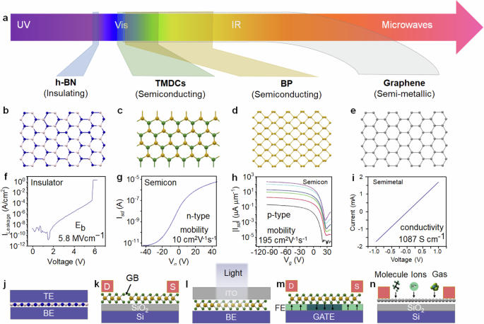
a Optical portion of the electromagnetic spectrum in UV, visible, and IR range. Molecule structure and corresponding electrical properties of insulating h-BN (b, f), semiconducting n-type TMDCs (c, g), semiconducting p-type BP (d, h), semi-metallic graphene (e, i). j–n Device applications of solution-processable 2D materials. j RRAM. k Memtransistor. l photodetector. m Ferroelectric field-effect transistor (FET). n Sensor. Panel g reprinted with permission from ref. 65., Springer Nature Limited; Panel h reprinted with permission from ref. 67., Wiley-VCH2021; Panel f reprinted with permission from ref. 126., American Chemical Society; Panel i reprinted with permission from ref. 133., Wiley-VCH2021.
Semiconducting TMDCs with desirable bandgaps, such as monolayer MoS2 (1.8 eV) and WS2 (2.1 eV), MoTe2 (1.1 eV) and WSe2 (1.7 eV) represent a compelling class of materials for various electronic applications. These 2DMs consist of layers of transition metal atoms sandwiched between chalcogen atoms, forming a hexagonal lattice structure (Fig. 4c). The unique atomic arrangement in TMDCs gives rise to an unprecedented layer-dependent electronic structure, where a transition happens from an indirect bandgap in bulk to a direct bandgap in monolayer, a feature not seen in traditional bulk semiconductors. This change in band structure results in strong light-matter interaction, rendering them promising candidates for photonics and optoelectronic devices (Fig. 4l). With sizable band gaps and high mobility, TMDCs especially MoS2 and WS2, are excellent candidates for logic gates to provide high-switching speed with low power consumption. Through solution processing, their nanosheets have demonstrated decent mobility ranging from 1 ~ 10 cm2V−1s−1 and a large on/off ratio (106) in thin film transistor arrays (Fig. 4g)39,65. Most solution-processed TMDCs show electron transport behavior due to the chalcogenide vacancies introduced during the exfoliation. BP, another representative 2DM with puckered structure and anisotropic electronic properties, offers hole conduction with excellent mobility of around 200 cm2V−1s−1(Fig. 4d, h)67. Those complementary metrics offered by TMDCs and BP meet the requirement for logic gate applications, and enable basic sensors for light, pressure and chemicals (Fig. 4n). When coupled with a ferroelectric HfZrO switching layer131,132, the semiconducting 2DMs FET enables ferroelectric polarization switching with a high on/off ratio and negligible degradation in endurance and retention properties for non-volatile multilevel data storage (Fig. 4m). In addition, analogous to the grain boundaries-assisted resistive switching (RS) in CVD-grown 2D film, the edge defects of the liquid-exfoliated 2D nanosheets, facilitate ion’s interlayer diffusion in conductive filament, and thus present an efficient way for the modulation of RS characteristics33 (Fig. 4k).
Graphene, composed of a single layer of carbon atoms arranged in a hexagonal lattice, has attracted significant attention for its exceptional properties, making it a widely studied material in recent decades (Fig. 4e). The carbon atoms in graphene are characterized by sp2 hybridization. This configuration results in three localized σ bonds on the flat surface and a delocalized π bond perpendicular to it. Ideal monolayer graphene exhibits a semi-metallic nature with zero bandgap, arising from the symmetry of the honeycomb lattice at the k-points of the Brillouin zone. Consequently, graphene possesses the capability to absorb a broad range of light, spanning from ultraviolet (UV) to infrared (IR) wavelengths. A recent study highlighted the impressive electrical conductivity of 1087 ({rm{S}}cdot {{rm{cm}}}^{-1}) in exfoliated monolayer graphene nanosheets, achieved through the ammonium intercalation-based method (Fig. 4i)133.
Thin-film transistors
As shown in Fig. 5a, the evolution of solution-processable 2DM transistors shows a progressive trajectory from proof-of-concept single flake devices to wafer-scale devices and further extension to integrated circuits. For instance, MoS2 monolayers and few layers have been exfoliated in Na2SO4 aqueous solvent with large lateral size up to 50 µm134. Despite apparent limitations, including anodic oxidation by oxygen-containing radicals and possible phase transition induced by Na+ doping, individual FET made of these exfoliated MoS2 monolayers exhibit a high on/off ratio over 106 and a reasonable mobility of 1.2 cm2V−1s−1. Building upon this, pioneer work has been further reported to fabricate printed transistors consisting entirely of 2D nanocomposites, where liquid-exfoliated h-BN, graphene and TMDCs nanosheets serve as the dielectric, contact and semiconducting switching layer, respectively 90. However, broad thickness distribution due to the low yield of direct liquid exfoliation causes the printed 2D networks to have large disorder and high porosity (43–63%), resulting in poor charge transfer and low mobility of 0.1 cm2V−1s−1. Enabled by enhanced intercalation chemistry with the organic quaternary ammonium molecules, phase-pure few-layered MoS2 nanosheets with narrow thickness distribution are obtained with improved exfoliation efficiency65. The resulting thin-film transistor (TFT) arrays show a current modulation of >105 and a high mobility of 10 cm2V−1s−1. Furthermore, functional logic gates and computational circuits, including inverter, NAND, NOR, AND and XOR gates, and a logic half-adder have been demonstrated based on the MoS2 n-FET. This work opens a scalable pathway to high-performance logic applications using solution-processable 2D semiconductor dispersions. Subsequently, the solution-processed FETs are further extended to WSe2 and WS2 on both rigid and flexible substrate processed at low temperature ( < 120 °C) through Langmuir−Schaefer deposition41. The ionic-gated WS2 and WSe2 transistors show electron conduction and ambipolar conduction, respectively, with high mobility in the range of 2–16 cm2V−1s−1. However, to enable complementary integrated circuits, p-type 2D FET is necessary but challenging due to lack of stable p-type 2D semiconducting dispersions and controllable doping method, especially in solution. Therefore, a wet chemistry doping strategy has been developed by bromide molecule (Br2) treatment, where the empty Br2 ({{rm{sigma }}}_{p}^{* }) antibonding molecular orbital state introduces a shallow acceptor state of 0.08 eV above the valance band maximum of WSe235. The Br2-doped WSe2 FET shows an improved hole mobility of 27 cm2 V−1 s−1, on/off ratio of over 107 and a near-zero threshold voltage. 2D CMOS inverter composed of solution-processed MoS2 n-FET and WSe2 p-FET has been further demonstrated, showing a record high gain of 1280 at a drive voltage of 7 V. To achieve large scalability without sacrificing their performance, a commercial slot-die printing has been utilized to deposit semiconducting MoS2 layer and a unique dielectric layer, sodium-embedded alumina on 5-inch wafer125. The MoS2 FETs exhibit a record-high mobility of 80.0 ± 11.0 cm2 V−1 s−1, contributed by effective van der Waals sheet-to-sheet contacts of MoS2 nanosheets, the high capacitance as well as an energetically flat dielectric layer composed of sodium-embedded alumina.

a Solution-processed 2D logic devices which evolves from exfoliation of monolayer 2D nanosheets to wafer-scale 2D devices and logic circuits (top panel). From left to right in Panel a reprinted with permission from ref. 134. American Chemical Society; ref. 65. Springer Nature Limited; ref. 35., Wiley-VCH2021 and ref. 125. Springer Nature Limited. b Solution-processed 2D memory devices which witness an evolution from individual planar RRAM to wafer-scale arrays and 3D stacking (middle panel). From left to right in Panel b reprinted with permission from ref. 83. Springer Nature Limited; ref. 138. Wiley-VCH2021; ref. 143. Springer Nature Limited; ref. 33. Springer Nature Limited. c 2D materials-based sensors develop from simple sensing towards multifunctional flexible and stretchable capabilities, enabling smart sensing, embedded intelligence, as well as sensing-memory-computing fusion (bottom panel). From left to right in Panel c reprinted with permission from ref. 239. American Chemical Society; ref. 160. American Chemical Society; ref. 91. Wiley-VCH2022; ref. 165. AAAS. To be noted, the depicted timeline in the figure does not adhere to a one-to-one correspondence with the milestones of the key devices. Rather, it serves as a visual representation of the temporal progression from 2014 to 2024, highlighting significant milestones associated with the key devices. The alignment of these milestones along the timeline is intended to illustrate their relative importance and impact within the broader timeframe.
Resistive Random Access Memory (RRAM)
RRAM stands as a promising candidate for next-generation non-volatile memory devices, offering remarkable speed, endurance, and energy efficiency. The integration of solution-processable 2DMs plays a pivotal role in advancing RRAM technology, unlocking new opportunities for memory applications that exhibit outstanding performance while being cost-effective and compatible with the CMOS technique. Figure 5b summarizes the evolution of solution-processable RRAM. Previous investigations primarily revolved around resistive switching in graphene oxide nanosheets as active layers, either in isolation or in combination with polymers or reduced graphene oxides135,136,137. However, most of those studies only focus on the device fabrication without much concern on the performance enhancement, showing limited optimization window between endurance ( < 103 cycles), switching voltages (1 ~ 6.7 V) and memory retention ( < 104 s). Furthermore, a comprehensive understanding of the underlying switching mechanism is lacking. In this context, a novel approach utilizing solution-processed MoOx/MoS2 and WOx/WS2 heterostructures, sandwiched between two printed silver electrodes demonstrates significant breakthrough83. Schottky junction formed between the ultrathin oxide layer ( < 3 nm) and Ag interface is identified as an effective means for modulating resistive switching in the printed heterostructure RRAM. This configuration allows for an exceptionally low operating voltage of 0.2 V, an unprecedentedly dynamic resistance ranging from 102 to 108 Ω and the capability for multilevel operation. Time-dependent and temperature-dependent I–V measurement of the MoOx/MoS2 RRAM reveals that nanoionics transport in the oxide layers dominates the memory effect, where the oxygen vacancies migration causes the metal valence change between Mo6+ and Mo5+. Inspired by the printed 2D memristors, diverse solution-processed 2D materials and heterostructures have been studied for resistive switches, including TMDCs-based RRAM33,37,42,138,139, BP-based RRAM52,140 and MXene-based RRAM141,142 et al. Among them, the solution-processed TMDCs-based RRAMs stand out due to their stable chemistry and facile processability. Several milestones have been achieved with solution-processed 2DM RRAMs, e.g. large memory window ranging from 102–108 136, ultralow programming voltage down to 0.18V38, minimal switching energy of 2.6 pJ/bit and forming-free operation143. However, most of these reports focus only on individual devices without indication of device-to-device variation and circuit demonstration at large scale. Recently, the wafer-scale implementation of RRAM arrays has been demonstrated with spin-cast MoS2 nanosheets33. In-depth materials study and electrical measurement of the MoS2 nanosheets have provided physical insights into the underlying switching mechanism in the solution-processed MoS2 RRAM, where a unique inter-flake sulphur vacancies percolation causes the formation and rupture of conductive filaments. This represents an effective way for resistive switching modulation since the percolation path of sulphur vacancies can be controlled by the nanosheets geometry. This is also supported by the aerosol jet-printed WSe2 RRAM143, which shows well-preserved resistive switching with inert and non-mobile carbon-based electrodes rather than active Ag or Cu electrodes. This suggests that the resistive switching mechanism is intrinsic to the WSe2 switching layer, likely due to selenium vacancies. A detailed discussion regarding the charge transport mechanism can be found in Section “Physical insights into the charge transport mechanism in solution processable transistors, RRAM and sensors”. In addition, the spin-cast MoS2 nanosheets exhibit a high degree of plane-to-plane alignment, ensuring efficient charge transport and structural integrity. Benefiting from the robust structure and edge defect-assisted switching, the wafer-scale MoS2 memristor arrays demonstrate excellent endurance (107 cycles), long memory retention (10 years), low device variations, and a high analog on/off ratio33.
Apart from performance gains from vertical stacking of logic and memory units, the emerging RRAM devices described in the above section can be employed to compute and process data within the memory. This way of computing inspired by the parallel processing, low power consumption and adaptability of human brain is referred broadly as neuromorphic computing. Specifically, the physical property of the switching layer and its conductance modulation are exploited to mimic the synaptic property. On the device level, high performance including low switching energy is essential, else the energy savings from in-situ computation cannot be fully reaped. It is the atomically thin structure of 2D materials that makes them beneficial for neuromorphic devices—voltage scalability resulting in reduced power consumption and gate tunability leading to a greater number of analog states. In this regard, the recently reported implementation of spiking neural network with 2D–CMOS hybrid microchips using hBN as the active switching layer by Zhu et al. offers great promise129. Additionally, the synaptic properties of RRAM can be modulated by a combination of electrical and optical stimuli, resulting in enhanced data storage capability and allowing for the convergence of storage and computation with image sensors144,145. Notably, a compact, low power pixel sensor using MoS2 phototransistor146, a large-scale robust image sensor matrix with active pixels consisting of nanoporous MoS2 phototransistors147, an optoelectronic memory device enabled by tellurium-based 2D van der Waal structure for in-sensor reservoir computing148are some of the recently reported works.
Photodetector
Photodetectors are indispensable components of modern technology, enabling the conversion of light into electrical signals for applications in optical communication (where light signal serves as the carrier of encoded information) and remote sensing (where the light signals convey valuable data). Commercial photodetectors are mainly constructed from Si or Si-based compounds or III-V materials (e.g. GaAs and InGaAs)149,150. Unfortunately, Si has an indirect bandgap of 1.1 eV, which constrains the response range between 300 and 1100 nm. While the integration of III-V compound semiconductors with Si extends the photo response range towards the short-wavelength infrared (SWIR) spectrum, the fabrication processes for high-quality III-V materials are complicated, costly, and incompatible with the CMOS process. More importantly, the rigid nature of crystalline silicon, GaAs, and InGaAs semiconductors restricts their use in next-generation flexible and wearable electronics. Therefore, it is imperative to explore novel photoactive semiconductor materials that can overcome these limitations.
The introduction of 2DMs represents a transformative breakthrough in photodetector design, driven by their unique electronic and optoelectronic properties. These atomically thin materials exhibit quantum confinement effects, allowing for tunable bandgaps and remarkable photoresponsivity across a wide range of wavelengths151,152. In comparison to traditional production methods like mechanical transfer and CVD growth, the convergence of solution processing techniques with 2DMs opens new avenues for creating large-scale, cost-effective devices suitable for applications ranging from consumer electronics to industrial monitoring84,153,154,155. Diligent work has been undertaken to tailor and optimize various solution-processed 2DMs, a notable endeavor that involves engineering materials specifically matched to distinct spectral ranges. For example, graphene has an ultra-wide spectral range spanning from UV to THz frequencies, ultrafast carrier mobility ( ~ 200,000 cm2V−1 s−1), and high electrical conductivity. However, the gapless nature of graphene leads to a high dark current, significantly degrading its sensitivity and limiting the further development of graphene-based photodetectors. Consequently, other 2DMs, such as TMDCs and BPs have been investigated because of their tunable bandgap ranging from 0.3 eV to 2.0 eV, which enables high sensitivity in the visible and near-infrared (NIR) regimes155,156,157,158.
For example, photodetectors composed of individual MoS2 monolayer and few-layer flakes can achieve high photosensitivity up to 880 A/W at low illumination power156, fast response of 70 µs157 and high sensitivity of 7.7 × 10¹¹ Jones159 in the 400–700 nm wavelength range. Coupled with their extremely low noise equivalent power, MoS2 can be an ideal candidate for very low-level photo detection. However, early works on solution-processed MoS2 photodetectors show degraded photoresponsivity and sensitivity. For instance, the inkjet-printed MoS2 photodetector has been reported with maximum photoresponsivity of 50 mA/W160. The low photoresponsivity is possibly due to the residues from the polymer stabilizer and randomly aligned nanosheets, which hinder charge transport in the device. Additionally, the use of toxic solvent dimethylformamide, which has a high-boiling point in the exfoliation of the MoS2 nanosheets, requires time-consuming and expensive formulation process or relatively high temperature to dry, constraining the range of compatible substrates. To avoid the use of toxic solvent and polymer binders in the ink, water-based and biocompatible 2D crystal inks93 have been developed for a range of 2DMs dispersions, including MoS2, WS2, h-BN and graphene, allowing the further fabrication of all-inkjet-printed graphene/WS2/graphene vdW photosensors93. However, water with a high surface tension of around 70 mN/m, exhibits poor wettability on common substrates such as Si/SiO2, glass and polyethylene terephthalate after deposition, resulting in non-uniform material deposition. This highlights the importance of formulating the ink properties to improve film quality for high-performance photodetectors. Binary solvents composed of isopropyl alcohol and 2-butanol have been developed that enables uniform deposition of BP nanosheets on PET and glass substrate without the need for substrate pre-treatment53. The binary solvent mixture creates variations in solvent proportions across the droplet due to differing evaporation rates, with faster evaporating solvent concentrated at the center and slower evaporating solvent at the edges. This results in a temperature gradient and subsequent recirculation of Marangoni flow, preventing coffee ring formation and ensuring uniform material deposition. Therefore, the BP-based photodetectors achieved an improved responsivity of 164 mAW−1 with a broadband detection range from visible to near-infrared wavelengths.
Apart from optimization over the ink properties and individual flakes, further efforts have been made to develop vdW heterostructures for high-performance and broadband photodetectors beyond the current state-of-the-art photodetectors91. VdW heterostructures offer precise control over the choice of materials in different layers, allowing for the fine tuning of electrical and optical properties to meet specific requirements, such as multispectral sensing and processing. Extensive research into various vdW photodetectors161,162,163,164 have yielded exceptional performance metrics, including ultra-high responsivity, sensitivity, and remarkably broad spectral response. Nevertheless, the construction of vdW heterostructures from solution is still in its infancy stage. Recently, an all-solution-based process for wafer scale electronics based on lateral and vertical vdW heterostructures have been reported91. Enabled by the high yield of electrochemical exfoliation, atomically thin graphene, MoS2 and HfS2 nanosheets have been produced and stabilized in a low-boiling point alcohol. Those nanosheets are further assembled into lateral and vertical vdW heterostructures in a three-terminal transistor configuration, where graphene and MoS2 serve as contact electrode and semiconducting channel, respectively. For the dielectric layer, a high temperature annealing process at 500 °C under ambient conditions transforms the HfS2 thin film into a flat HfO2 layer with significantly reduced roughness. Notably, the wafer-scale transistor array exhibits record-high photoresponsivity ( ~ 7×10⁵ AW−1), outperforming most of the previously reported TMDC-based photodetectors156.
Moreover, the unique advantages offered by solution-processed 2D thin films extend far beyond the realm of photodetectors, exerting a transformative influence on a wide range of sensing applications, particularly within the context of the Internet of Things. In this dynamic environment, the attributes of solution-processed 2D thin films find a harmonious fit. As reported by Yan et al. 165, the absence of bonds between MoS2 nanosheets in vdW interfaces allows them to slide and rotate, resulting in remarkable mechanical flexibility, stretchability, and malleability. The staggered nanosheet arrangement also forms nanochannels, providing great permeability. These ultra-thin ( ~ 10 nm) and robust films can perfectly conform to soft biological tissues, adapting to microscopic surfaces and seamlessly integrating with living organisms. This leads to conformal interfaces that enable electronic functions within living organisms. In contrast, freestanding polycrystalline MoS2 thin films grown by CVD show poor flexibility due to stiff and strong covalent bonding within the grains and disordered bonds at their grain boundaries165. The exceptional adaptability of solution-processed MoS2 film empowers sensing devices to seamlessly conform to diverse physical environments, thereby enhancing their ability to capture accurate and reliable data. Furthermore, the capacity of solution-processed 2D thin films to maintain structural stability even in an ultrathin freestanding format offers a promising avenue for future monolithic 3D electronics. Traditional electronic devices often encounter challenges in integrating with complex geometries, limiting their potential for compact and efficient designs. Solution-processed 2D thin films, on the other hand, hold the potential to revolutionize this landscape. Their ability to conform to intricate shapes, combined with efficient charge transport across interfaces, opens the door to innovative designs that were previously constrained by the limitations of conventional materials.
Physical insights into the charge transport mechanism in solution processable transistors, RRAM and sensors
Through our previous discussions, we have unveiled the significant potential of solution-processable 2D materials and their diverse applications in logic, memory, and sensing. This section emphasizes the need for a deeper understanding of these materials, particularly their charge transport mechanisms of transistors, RRAM and sensors. Such understanding is pivotal for their overall performance, as 2DMs with different morphologies is required to address the conflicting charge transport attributes for logic and memory. Notably, transistors should be optimized for high performance and low leakage, while RRAM should be optimized for low-voltage defect-enabled switching ability. Regarding sensors, the percolating-film photodetectors provide unique opportunities to study and harness the interactions between light and the ley properties of solution processed films such as vacancies at the flake edges, lateral flake size and thickness. By employing a combination of materials characterization, we aim to shed light on the physical mechanism underlying the remarkable properties of these devices. Such understanding is critical, as it not only contributes to a fundamental understanding of these materials, but also holds the key to optimizing their performance across various applications.
Charge transport mechanism in solution-processed transistors
While extensive research has been devoted to understanding the conduction mechanism in isolated 2D flakes166,167, it becomes more complicated in the case of solution-processed transistors. The complexity arises from the interplay of multiple physical processes—a consequence of the disordered and polycrystalline nature inherent to the nanosheet networks. As discussed in Section “Materials synthesis and deposition”, the solution-processed 2DM composite film comprises disordered nanosheet networks connected via junctions of narrow vdW gap with some degree of in-plane alignment. At a mesoscopic level, the electronic conduction in these films involves contribution from nanosheet resistance (RNS) as well as the junction resistance (RJ) (Fig. 6a). While RNS is a material-dependent property, RJ is attributed to the inter-flake resistance at the overlap region between two flakes and thus is dependent on the quality and morphology of the junction. Consequently, the limiting factor for conductivity is dependent on the relative magnitude of RNS and RJ, which allows us to describe two conduction regimes of operations—junction-limited conduction (RJ »RNS) and material-limited conduction (RJ «RNS)123. Efforts to characterize and quantify the local junction resistance using conductive atomic force microscopy (C-AFM) current mapping have been reported (Fig. 6b). For instance, Nirmalraj et al. 168 investigated the junction resistance between the flakes in a solution-processed graphene film. As the C-AFM cantilever traces the junction between the flakes, the current map indicates a high voltage drop across the flake intersection. The corresponding junction resistance is found to be ∼550 Ω and ∼6.5 kΩ for a network of monolayer and multilayer graphene, respectively168. On the other hand, to investigate the intra-flake properties such as photoconductivity dynamics, optical-pump terahertz (THz)-probe spectroscopy is widely employed (Fig. 6c)169. Owing to the transient nature of THz pulses, the optical excitation injects charge carriers that are driven over a short distance (tens of nm), thus capable of unveiling properties of intra-flake transport. Additionally, the temperature-dependent photoconductivity analysis offers an effective way to deconvolute the contribution of intra-flake properties from the total conductivity169. As shown in Fig. 6d, the photoconductivity of MoS2 nanosheets increases as the temperature is reduced, indicating that the intra-flake transport characteristics are dominated by phonon scattering limited band-like transport169.

a Schematic representation of nanosheet network as a resistive network comprising of nanosheet resistance (RNS) and junction resistance (RJ). b C-AFM is employed to map the junction resistance via current mapping across the inter-flake junction. c Schematic illustration of optical-pump–THz-probe spectroscopy on 2D material systems. d Photoconductivity dynamics of MoS2 nanosheet using THz pump-probe spectroscopy under different temperatures. Reprinted with permission from ref. 168, American Chemical Society 2011. Reprinted with permission from ref. 169, Wiley-VCH2023.
As shown in Fig. 7, attempts to characterize the charge transport mechanism in solution-processed logic devices based on a combination of temperature and electric-field-dependent measurements have been reported170,171,172. Erik Piatti et al. 172 investigated the charge transport mechanism of surfactant and solvent-free inkjet-printed MoS2 films using temperature and gate dependent conductivity. As shown in Fig. 7a, inkjet-printed MoS2 transistors exhibit a gate-induced crossover from hopping at low gate voltage to band-like transport at high gate voltage. These features indicate charge transport occurring in two distinct regimes: an insulating phase characterized by hopping transport, and a metallic phase involving transport over extended states. The separation between these phases is marked by the insulator-to-metal transition at Vg = 1.37 V, governed by the ratio of intra- and inter-flake conductance. Figure 7b shows the plot of conductivity (σ) against T(-1/4) for a representative MoS2 ungated device, where the logarithm of σ scales linearly with T(-1/4) for temperatures up to 200 K, suggesting 3D Mott Variable Range Hopping (VRH) conduction. Similar transitions from Mott VRH at low temperatures to nearest neighbor hopping (NNH) at high temperatures have been documented in disordered MoS2 flakes166,173. A benchmark plot of activation energy values observed in disordered and isolated MoS2 flakes under gated and ungated condition are shown in Fig. 7c. The notably elevated activation energy obtained in MoS2 networks suggests that the conduction is primarily dominated by inter-flake hopping.

a–c Charge transport mechanism in solvent-free 2D films. a Conductivity vs gate voltage of printed MoS2 transistors measured at different temperatures. b Conductivity as a function of T-1/4 for an ungated MoS2 device to determine the reduced activation energy. c Activation energy (Ea) as a function of gate voltage in different MoS2 devices. d–f Charge transport mechanism in covalent-interconnected 2D network film. d Schematic representation of inter-flake transport facilitated by vacancy healing mechanism and covalent interconnections in MoS2 films by aliphatic PDT and aromatic BDT molecules. e Conductivity vs temperature plot for MoS2 films, MoS2–PDT networks, and MoS2–BDT networks. f Extrapolated average Rhop for MoS2 films, MoS2–PDT networks, and MoS2–BDT networks, accompanied by an illustration of their respective hopping mechanisms. Figures a-c reprint with permission from ref. 172, Springer Nature Limited. Figures d–f reprint with permission from ref. 169, WILEY-VCH 2023.
Recently, molecular functionalization has been explored as an effective strategy to overcome limitations of high inter-flake junction resistance and disorder109,169. The functionalization serves not only to heal the disorders, but also facilitates the proximity of adjacent flakes, promoting the formation of a covalent interconnection of TMDCs. For instance, by employing multi-scale analysis, aromatic-conjugated 1,4-benzenedithiol (BDT)) versus aliphatic 1,3-propanedithiol (PDT) linkers have been investigated on MoS2 nanosheet films109,169. Primarily, through temperature-dependent scattering time analysis, the scattering rate for MoS2–BDT is found to be 40% less than pristine MoS2 films, indicating the beneficial role of the thiol group in healing vacancies. Figure 7d shows a schematic representation of the healing mechanism and covalent network interconnection in pristine MoS2 films utilizing aliphatic PDT and aromatic BDT molecules, focusing on inter-flake charge transport. According to the temperature-dependent conductivity of MoS2, MoS2–PDT networks, and MoS2–BDT networks, two distinct operational regimes are observed (Fig. 7e). In the high-temperature range (200K–340 K), the conductivity exhibits an exponential dependence on temperature, indicative of a thermally activated hopping regime. Conversely, in the low-temperature range (5 K–150 K), conductivity remains independent of temperature, suggesting a tunneling regime of operation.
The extrapolated average hopping distances (Rhop) for MoS2 films, MoS2–PDT networks, and MoS2–BDT networks, accompanied by an illustration of their respective hopping mechanisms are shown in Fig. 7f. Pristine MoS2 exhibits Efros–Shklovskii variable range hopping (ES-VRH), where the hopping transport is governed by the Coulomb scattering of the charge carriers interacting with fixed charge centers. Conversely, in MoS2–PDT networks, the sulphur vacancies are healed by the aliphatic PDT molecules, neutralizing the Coulombic scattering centers, which shifts the charge transport mechanism from ES-VRH to 3D Mott Variable Range Hopping (3D Mott VRH). In the case of MoS2-BDT molecules, the carrier dynamics is characterized by nearest neighbor hopping (NNH), where the charge carriers hop between the two spatially nearest trap sites, regardless of their energy levels. Here, the aromatic ring plays a crucial role in enhancing inter-flake transport by connecting two adjacent flakes and improving their electronic connectivity by establishing a favorable conduction path for the charge carriers. Thus, in contrast to solvent-free MoS2, the charge transport in covalent network-based MoS2 is primarily governed by an inter-flake hopping mechanism, whose characteristics are significantly influenced by the chemical structure of the linker.
These investigations emphasize the necessity for a comprehensive characterization of the charge transport dynamics throughout the nanosheet network to reveal the interplay between charge carrier dynamics across the junctions (inter-flake transport) as well as carrier transport within each flake (intra-flake transport). This is particularly crucial as inter-flake transport through hopping or tunneling across junctions can significantly affect mobility and device-to-device variability that are key to wafer-scale integration and performance reliability. Nevertheless, the investigation of charge transport properties of nanosheet networks is still in the early stage of development. The polycrystalline nature and the complexities related to ink formation and different deposition methods have posed challenges in investigating the charge transport behavior in solution-processed 2D transistors. Employing diverse techniques, including temperature-dependent, magnetic-field-dependent, and electric-field-dependent measurements, is essential to unveil the complete mechanism. Additionally, careful consideration of the contribution of disorders, such as sharp boundaries between different printed flakes, is essential.
Charge transport mechanism in solution-processed RRAM
As opposed to logic devices, where defects are detrimental to operations, defects such as sulphur vacancies in MoS2 introduced during liquid phase exfoliation, play a crucial role in the switching kinetics of memristive devices33. However, the resistive switching mechanism in solution-processed memristors remains poorly understood. Unlike crystalline or amorphous materials, resistive switching in 2D nanosheet networks is uniquely influenced by nanosheet dimensions and percolation path morphology. This is a unique characteristic potentially observed only in solution-processed thin films33. Moreover, the understanding of the switching mechanism is further complicated by the presence of electrochemically active metal electrodes. This is because the dynamics between metal ions vs vacancies transport in the active region that eventually constitutes the conductive filament remains elusive38,143. In this section, we unveil the resistive switching mechanism in solution-processed RRAM through a synergistic approach that combines in-situ material characterization and physical modelling. Such fundamental understanding of the factors that influence the resistive switching mechanism is crucial for optimizing device design and maximizing device functionality.
In-situ characterization and physical modelling
Several in-situ characterization and visualization techniques have emerged as key approaches in investigating the switching mechanism in memristive devices. The techniques reported for solution-processed memristive devices is shown in Table 1. Importantly, they provide critical information about the process of resistive switching, nanoscale morphology, constituent of conducting filament and their interfaces. Among these, in-situ conductive atomic force microscopy (C-AFM) is a versatile technique that captures local morphological, topographical changes and determine the location of conductive filament by probing the local current across the active area. Feng et al. 38 employed such C-AFM current mapping and reported that faster switching with high current density is related to defective locations within the inkjet-printed MoS2 switching medium. Additionally, in-situ Kelvin probe force microscopy (K-PFM) enables surface potential mapping and provides insights on vacancy dynamics, quantification of vacancies, trapping/de-trapping of space charge, etc. Furthermore, Tang et al. 33 employed in-situ K-PFM characterization in combination with C-AFM analysis to reveal the presence of sulphur vacancies at the flake edges of solution-processed MoS2 films and vertical percolation across the stacks. In-situ thermal imaging of filaments by an infrared video camera enables direct monitoring of device temperature and can provide qualitative insights on thermal-assisted switching174. While in-situ PL spectroscopy can characterise localized oxidation in the film during switching, dark field and bright field optical micrograph can aid in visual inspection of features in the channel including filaments and dendrites on a slightly larger spatial resolution174.
However, owing to the buried channel and inaccessibility of the active area, two terminals vertical memristors are not suitable for most of the in-situ characterization techniques such as K-PFM, C-AFM, etc. Hence visualization efforts on vertical memristors are majorly focussed on post-mortem imaging of devices which, however, fails to capture the dynamic process of defect migration. Thus, due to the limited temporal resolution, the investigation of vacancy kinetics and transportation over time (retention), repeated cycling (endurance), etc is challenging. Additionally, the spatial resolution in most of the techniques is limited to a few micrometres and is particularly a concern in solution-processed films since the percolating nanosheet network may exhibit a switching mechanism different from individual flakes.
Simulation and modelling, on the other hand, are inevitable tools that offer timely and cost-effective approaches to support the experimental investigation175,176. The demand is for a multi-scale modelling strategy that can describe the physical details of the materials as well as capture the high-level description of system-level operations. Accurate physical models can aid in the investigation of the dynamic resistive switching, providing insights on intermediate conductive filament growth/rupture mechanisms and the interplay between dominant driving forces (e.g. electrical vs. thermal) at a larger spatial and temporal resolutions than those achievable with in-situ characterization techniques. Crucially, vacancy migration and interface barrier adjustments across the percolating network, which are difficult to observe with in-situ characterization techniques, can be reconstructed with a physical model. Different modelling approaches in terms of computational cost and accuracy are summarized in Table 2.
Recent studies have unveiled the switching mechanism in solution-processed memristive devices through atomistic modelling. Only a few research groups have undertaken Density Functional Theory (DFT) calculations to derive the diffusion barrier for vacancies as a function of different percolation paths and flake geometric features such as lateral flake size. With the presence of an electrochemically active metal, Feng et al. 38 reported that sulphur vacancies in MoS2 allow ion penetration of active metal (Ag ion) along the vertical and lateral gaps of MoS2 flakes, forming a conductive filament. The diffusion barrier for all the plausible percolation paths (Fig. 8a) for the Ag metallic ion, as determined by DFT calculations is shown in Fig. 8b. The horizontal percolation path for Ag ion through the bottom-top gaps and the interlayer space of multilayer MoS2 flakes are depicted by PL1 and PL2, respectively. Ag metallic ions can also diffuse both horizontally and vertically across the Mo- and S-member rings in the directions of PH1 and PH2, respectively. Importantly, Ag prefers to substitute for S position to generate an Ag substitutional defect, and S atoms facilitate Ag diffusion. It should be noted that the energy barrier for Ag ion to diffuse into the MoS2 interlayer is as high as 1.3 eV (the L21 path), and that the energy barrier for Ag ion to diffuse through the Mo- and S-member rings within internal layer of a MoS2 flake is as high as 8.41 eV. Such high diffusion barrier essentially rules out the possibility of vertical diffusion of Ag ions in the interlayer space of multilayer MoS2 flake. On the other hand, the Ag diffusion steps for L11, L12, and L22 path have an extremely low diffusion barrier of 0.29 eV. Therefore, horizontal diffusion via the bottom-to-top gaps and vertical diffusion through the side gaps are the most energetically advantageous routes for Ag ions to produce Ag filaments. Furthermore, Tang et al. 33 investigated the geometric effect of MoS2 nanosheet flakes on the sulphur vacancy diffusion barrier using DFT calculations (Fig. 8c). As shown in Fig. 8d, the diffusion barrier for sulphur vacancy decreases as flake size of MoS2 decreases. For instance, the diffusion barrier of 0.75 eV is reported for a lateral flake size of 0.48 μm. Such correlation between nanosheet size effects and the sulphur vacancy diffusion barrier offers additional tuning knob to the engineer the functionality and resistive switching mechanism in solution-processed memristors.

a Schematic of different percolation path for Ag ion in a MoS2 stack. b The corresponding diffusion barrier energies for the different percolation path shown in b based on KMC and DFT simulations. With the least energy diffusion barrier found for L11 and H11, the most energetically favourable paths are horizontal percolation through the bottom-top gaps and vertical diffusion through the side gaps. c Schematic representation of vacancy percolation path with small MoS2 flake size (top) and large MoS2 flake size (bottom) d Effect of vacancy diffusion barrier on the MoS2 flake size. The diffusion barrier decreases as the lateral flake size reduces. Panel a, b reprint with permission from ref. 38, Wiley-VCH2021; Panel c, d reprint with permission from ref. 33, Springer Nature Limited.
However, the efficiency of physical models for resistive switching is strongly influenced by specific material properties, such as thermal conductivity, stoichiometry, vacancy mobility, and defect concentration. Accurate experimental characterization of these parameters is essential for enhancing model precision, especially for solution-processed films where material properties may exhibit anisotropy, such as anisotropic in-plane and out-of-plane thermal conductivity177. While physical models are crucial for compact modeling, they must be validated by experimental data. For instance, the initial vacancy distribution is often assumed to be uniform, which may not always reflect reality. Techniques such as K-PFM178, Raman and photoluminescence spectroscopic characterization179 can be used to accurately determine the initial distribution. This integrated approach that combines in-situ characterization with device modeling, is essential for gaining a deeper understanding of vacancy migration and its coupling with electron transport. It is also worth noting that a comprehensive understanding of resistive switching remains elusive, primarily due to the limited availability of experimental data on critical aspects like switching dynamics. This includes the evolution of filament morphology and transport mechanisms during repeated cycling. Device modeling can help bridge these gaps by extending both the temporal and spatial resolution of the analysis.
Towards this end, efforts to realize an effective convolution of in-situ characterization and device modelling to enable optimized device design and maximize the device functionality deserves keen attention180. A schematic overview of such an approach with spatiotemporal resolution ranging from materials to circuit level is shown in Fig. 9. Atomistic simulations based on DFT can determine the physical quantities such as the formation energy of vacancies and diffusion barriers for vacancy migration that are critical to simulate device operations33,38. Physics-based models for device simulations using finite element methods (FEM) and kinetic monte carlo (KMC), provide physical insights on a larger spatial scale (on the scale of tens of cubic nanometers). FEM models involve solving a set of transport equations for vacancies, carriers, and lattice temperature self consistently with a continuous description of defect concentration175,176. In contrast, KMC models rely on discrete individual defects and inherently incorporate stochastic behaviour181. Characterizing the spatial distribution of vacancy concentration, electric field, lattice temperature, and key parameters such as in-plane and out-of-plane thermal conductivity from various in-situ techniques is crucial for the accuracy of physics-based models. Finally, compact models provide a simplified representation of the resistive switching mechanism by incorporating inputs from physics-based models and empirical assumptions182,183. These compact models are used for circuit and system-level simulations, offering reduced computational costs.

Leveraging the spatiotemporal resolution of each technique, the integrated approach can be used to investigate the RS mechanism and enable optimized device design. Physics based models are implemented with inputs from atomistic simulations and in-situ characterizations. Following this, compact models are employed for circuit and system-level simulations with low computational costs.
Flake Size and Thickness Dependent Switching
From the reported works, it is understood that the key factors that govern the RS mechanism are the lateral size of individual flakes, the thickness of the switching medium, and the efficacy of active metal ion diffusion across the switching layer. Tang et al. 33 have reported that lateral flake size optimization in solution-processed nanosheets offers a unique approach to modulating the RS mechanism controlled by the inter-flake vacancy diffusion and edge defect density. In-situ K-PFM characterization in combination with C-AFM analysis revealed the presence of sulphur vacancies at the edges supporting the argument that the RS is attributed to the vertical percolation of sulphur vacancies across MoS2 stacks along the flake edges. Importantly, investigation on the RS mechanism for varying lateral size distribution centered at 0.48 μm, 1.20 μm, and 2.40 μm revealed a strong correlation between nanosheet size and RS mechanism—reducing the average nanosheets size (λ) results in a reduced set/reset voltage (Vset/Vreset) and their cycle-to-cycle variations (Fig. 10a-c). Those findings related to flake size dependent switching are summarized in Fig. 10g. Smaller flakes exhibit higher sulphur vacancy density due to the increased edge-to-basal plane ratio, leading to a reduced set voltage. Furthermore, Tang et al. 33 found smaller MoS2 flakes offer a reduction in cycle-to-cycle switching variations attributed to more uniform and smoother average percolation length of sulphur vacancy. In contrast, larger flakes suffer from higher randomness, resulting in greater cycle-to-cycle switching variations.
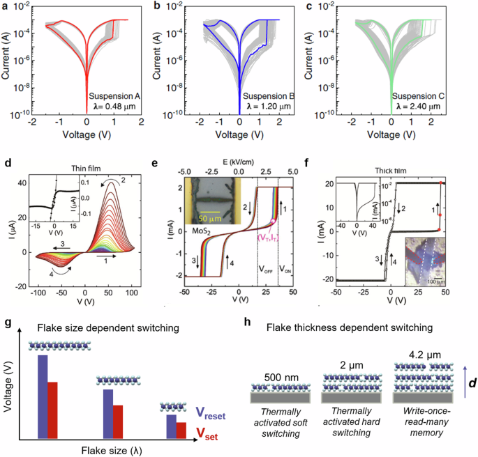
a-c I-V curves of MoS2 memristors made from suspensions with lateral flake sizes of 0.48 µm, 1.2 µm, and 2.4 µm, respectively. d For d < 500 nm, a thermally activated soft switching is observed with I-V characteristics exhibiting the NDR feature. e For d = 1-2 µm, a volatile RS and thermally activated hard switching are observed. f For d > 4 µm, the bulk conductivity ≈ 0.4 S m−1 and an irreversible and abrupt increase in conduction at V = VON is observed corresponding to write-once-read-many memories. g Dependence of lateral flake size on Vset and Vreset voltage. Smaller nanosheets correspond to higher Vs density due to the larger edge to basal plane ratio, resulting in smaller set voltage. h Dependence of flake thickness on the nature of resistive switching. Panel a-c reprint with permission from ref. 33., Springer Nature Limited. Panel d-f reprint with permission from ref. 174., Wiley-VCH2021.
Furthermore, Sangwan et al. 174 investigated the thickness dependent switching mechanism of the MoS2 percolating films by using the electrochemically inert gold electrode. The RS mechanism is proposed to originate from thermally activated electric discharge in the gaps between nanosheets with small radii of curvature under a large electric field. Accordingly, the switching behavior differs from the conventional non-volatile bipolar behavior reported by other works33,140,184. Depending on the nanosheet film thickness (d) and their corresponding bulk conductivity, three different regimes of switching behavior were reported (Fig. 10h). Specifically, for d = 1-2 µm, thermally activated hard switching and volatile RS are observed. As shown in Fig. 10d, the device switches from a high resistance state to a low resistance state at a voltage VON for positive voltage and upon decreasing the voltage, the device transforms back to another high resistance state at a voltage VOFF. Similar switching behavior is observed in the negative bias sweeps with an ON-OFF ratio of 100. Modulating the sweep bias range (VMAX) in the vicinity of VT (the voltage just before switching), further provides insights into the critical role of temperature on the RS as shown in the inset of Fig. 10d. For VMAX < VT, the current continues to increase at decreasing voltage, representing a dynamic negative differential resistance (NDR), however, the compliance current is not yet reached. At VMAX = VT, a much more prominent NDR behavior is observed and for VMAX > VT, the characteristics begin to follow the standard RS behavior. The device has thus attained a crucial local temperature for thermal runaway at VT, which is a point of no return. For d < 500 nm, a thermally activated soft switching is observed, wherein the I-V characteristics are similar to the NDR feature observed in hard thermistor memristor for VMAX < VT except for the fact that the current does not reach the compliance current even for very high lateral bias (Fig. 10e). For d > 4 µm (bulk conductivity ≈0.4 S m−1), an irreversible and abrupt increase in conduction at V = VON is observed whose characteristics are similar to write-once-read-many (WORM) memories (Fig. 10f).
While TMDCs like MoS2, WS2, and WSe2 exhibit similarities in their fundamental charge transport mechanisms, particularly in RRAM devices where conductive filaments form through vacancy migration, it is important to acknowledge that differences in material composition and defect chemistry can lead to variations in these mechanisms. For example, in MoS233, charge transport is driven by sulfur vacancies, while in WSe2143, it is driven by selenium vacancies, both of which migrate to form conductive paths. However, the vacancy densities dictated by the exfoliation process and their migration pathways can differ between these materials, potentially leading to variations in their resistive switching behavior. As a result, although the general mechanisms—such as vacancy migration and filament formation—are similar across TMDCs, detailed studies are required to fully understand the specific charge transport characteristics of each material.
As for other 2D materials, like BP and h-BN, are far less explored in the context of solution-processable electronic devices due to inherent challenges. For example, BP suffers from significant stability issues, especially in ambient conditions, which limit its use in long-term applications. Meanwhile, h-BN with a wide bandgap (5.95 eV) has poor conductivity and strong interlayer bonding185, making electron injection difficult and complicating liquid exfoliation processes124. Consequently, there are limited reports on electronic devices from solution-processed h-BN films. Nevertheless, as exfoliation techniques for h-BN and chemistry for stabilizing BP advance, investigating the charge transport mechanisms in h-BN and BP devices could yield valuable insights into their potential applications.
Charge transport mechanism in solution-processed sensors
In this section, we briefly discuss the charge transport mechanisms in solution-processed sensors, specifically photodetectors, although 2D materials are also widely used in applications such as gas sensors186,187. The central question here is to understand the fundamental differences in charge transport mechanisms between solution-processed devices and their conventional counterparts and how we can exploit them to our advantage. While many papers focus on performance metrics, the photoconduction mechanism in solution-processed materials remains underexplored. Key factors such as defect-mediated light absorption, flake size, thickness, and vacancies at the flake edge play crucial roles in determining photodetection performance. We review recent works that explore these mechanisms and attempt to characterize the charge transport properties in such systems.
Kim et al. reported that a chemically welded, solution-processed MoS2 photodetector exhibited a photoresponsivity of 1.7 A·W−1 in both the visible and NIR regions188. The enhanced performance was attributed to the formation of additional sulfur vacancies during annealing under H2/Ar conditions, which created two unoccupied states approximately 0.63 eV below the conduction band edge. These states originate from the dangling bonds of Mo 4d orbitals due to unsaturated charges, as well as a shallow state near the valence band. The introduction of these defect states supports a super linear intensity dependence of photocurrent, explained by a two-center Shockley-Read-Hall (SRH) recombination process. As laser intensity increases, quasi-Fermi level splitting rises, populating sensitizing centers near the valence band with holes, which serve as recombination centers, thereby reducing overall charge recombination losses. In addition to the SRH process, photothermal effects also contribute to the overall response, which is primarily dominated by a hopping transport mechanism.
Photogating is another significant mechanism in photodetectors. For instance, an all-solution-processed MoS2 transistor array, when exposed to light at wavelengths of 655 nm, 520 nm, and 450 nm, achieved an impressive maximum photoresponsivity of approximately 7 × 10⁵ A·W−1 under 655 nm illumination, with a power density of 0.59 μW·cm−2, at gate voltage of 1 V and drain voltage of 0.1 V91. The optical response of the device was explored by applying a gate voltage under fixed-wavelength illumination. As the power density increased, the threshold voltage shifted negatively, indicating a strong photogating effect. The exceptional photoresponsivity can be attributed to the channel’s composition, predominantly consisting of monolayer MoS2 nanosheets. These nanosheets exhibit a higher quantum yield compared to few-layer TMDCs. Additionally, the photoactive layer is 7–8 times thicker than typical monolayer TMDC photodetectors, enhancing light absorption and contributing to the device’s superior performance. In the accumulation regime (VG = 1 V), the power density-dependent photoresponsivity followed R ≈ P-0.7, while in the depletion regime, a weaker dependence of R ≈ P-0.4 was observed. The deviation from the ideal power-law behavior (R ≈ P0) is attributed to defect states introduced into the bandgap, which contribute to charge trapping and recombination.
Coupling light with RRAM can enable them to act as sensors. Zefeng et al. 42 studied solution-processed MoS2 optical RRAM and found that resistance switching and optical response are driven by vacancy migration and photon-induced heat. Under illumination, the dependence on external bias weakens, resulting in a reduction of the set voltage. During the SET process, the applied bias reduces both the width and height of the Schottky barrier, enhancing electron thermal emission and increasing the tunnelling probability, which leads to improved current. Concurrently, positively charged sulfur vacancies migrate along the edges of MoS2 sheets under the influence of the voltage bias, eventually connecting the top and bottom electrodes and creating a conductive pathway through the MoS2 layers. As a result, the device transitions from a high resistance state to a low resistance state due to more tunnelling electrons, which is facilitated by a greater concentration of vacancy defects (quasi-continuous defect levels) in the pathway. Under illumination, the increased carrier concentration raises the current and generates more heat through Joule heating. This heating, along with optical power dissipation, accelerates the movement of sulfur vacancies, forming a denser defect level. Consequently, the dependence on external bias diminishes, causing the VSET to decrease under illumination.
Recently, an anomalous photocurrent behavior has been observed in solution-processed self-powered photodetectors fabricated using WS2 nanosheets in a vertical structure189. These devices exhibit a fast photo response within milliseconds under pulsed illumination but display an anomalous slow decay of photocurrent during the pulse width (pulse-on time ~50 s). Time-dependent photocurrent measurements under varying illumination intensities show that charge accumulation and trapping occur at the interfaces, which act as recombination centers, leading to charge carrier recombination losses. Comparing the external quantum efficiency spectra with absorption data reveals that, while WS2 nanosheets absorb light in the higher wavelength range (700–850 nm), photocurrent generation in this region is less efficient than in the lower-wavelength range. This reduces efficiency because in the higher-wavelength region, absorption is dominated by trap excitations, which generate either holes or electrons. One of the photogenerated charges is subsequently trapped in these states and cannot be effectively collected at the electrode, particularly as the photodetector operates in self-powered mode.
While the above discussed papers attempt to understand the photocarrier generation and transport mechanisms, the complete picture remains unclear. To fully understand these interactions, comprehensive material characterization and advanced modeling are necessary. Techniques such as time-resolved photoluminescence, photoluminescence, and exciton dynamics studies are essential for investigating photocarrier generation and transport mechanisms. Furthermore, first-principles simulations, including DFT provide valuable insights into how vacancies and edge configurations influence the electronic structure and light-matter interactions in 2D materials. These simulations help clarify changes in electronic states, band structures, and exciton dynamics due to defects, aiding in the design of more efficient solution-processed sensors. This is an area that warrants greater attention from the materials research community.
Materials-device-system Co-integration
The growing demand for modern applications emphasizes the necessity of hardware architectures and technologies that can deliver exceptional performance while consuming minimal power. These architectures must be optimized for data-centric operations, enabling efficient deployment of intelligence at the edge, as well as the extraction and fusion of information from numerous sensors190. Remarkably, the number of sensory nodes is experiencing an exponential surge, projected to reach 75 billion by 2025 and expected to skyrocket to 125 billion by 20304. A significant portion of the analog data generated by these sensory nodes is unstructured and redundant. Therefore, it becomes imperative to not only explore cost-effective and practical methods for integrating new materials on silicon CMOS wafers, but also to devise novel mechanisms and architectures capable of efficiently processing sensory data within this evolving computing paradigm. This is particularly crucial in addressing the significant latency issues caused by data shuttling between separated memory and processing units in the conventional Von Neumann architecture.
In this section, we will look at the advantages of solution-processed 2DMs in contemporary non-von Neumann computing solutions as well as heterogeneous integration with existing silicon technologies. We will also propose potential research directions that would complement efforts in materials-device-system co-integration moving forward.
Novel computing system and architecture
Memristors for in-memory computing
Among all the current state-of-the-art non-von Neumann computing architectures, in-memory computing using memristor crossbar arrays is known to be one of the most area and energy-efficient methods191,192. By leveraging on electric field induced non-volatile conductance changes in individual memristors and Kirchoff’s laws, vector-matrix multiplication (VMM) can be computed in a one-shot and largely parallel fashion that cannot be done with traditional logic-based computational systems193. Currently, such memristor crossbar arrays are commonly implemented with oxide-based resistive switching memories. A recent work from Cai et al. 194 showcased a 20 by 20 WOx memristor crossbar array that has been integrated with CMOS-based peripheral circuits to perform on-chip multiply-accumulate and VMM operations. However, this demonstration also highlights the fact that the effectiveness of the system level computation is limited by the intrinsic variability of the memristor device192. Specifically, Cai et al. 194 has shown that the cycle-to-cycle and device-to-device variations have limited the size of the models that can be computed using the memristor array. Thus, controlling variability between device and resistive switching cycles has been of great research interest. Through this example, the need for materials-device-system co-optimization is also emphasized. With respect to the issue of controlling variability between devices and cycling, spin-coated MoS2 nanosheets thin films with controllable cycle-to-cycle variations through flake size modulation have been demonstrated to be a potential solution as shown in Section “Physical insights into the charge transport mechanism in solution processable transistors, RRAM and sensors”33. The unique resistive switching mechanism provides a fresh perspective in expanding the capabilities of the system-level computation with a device solution.
The application of solution-processed memristors holds promise for achieving flake size dependent resistive switching characteristics. However, overcoming the limitations of these devices requires a systematic approach, particularly through system-level strategies like monolithic stacking. An early work by Sivan et al. 143 explores this aspect, specifically targeting the challenge of insufficient drive current in aerosol jet-printed WSe2 memristors. This issue arises due to the shrinking cell size in a one-transistor-one-resistor architecture within future scaled technology nodes. Scaling down the memory cell size is necessary to deliver dense memory architectures with reduced device-to-device variations. Nevertheless, this reduction in memory cell size implies a decrease in transistor width, leading to the degradation of transistors’ drive current. In response, Sivan et al. 143 proposed a concept of stacked WSe2 FET channels with a vertical gate-all-around configuration. This approach ensures sufficient drive current without compromising the planar cell size (Fig. 11a). This is an example of leveraging system design to address problems on a materials-device level. Similarly, to overcome limitations in storage capacity per planar area in memristor devices, 2DM-based M3D memory cubes have been further demonstrated at the device level through sequential deposition of metals and spin coating of MoS2 layers33 (Fig. 11b). Each layer of the MoS2 RRAM memory cube can be independently programmed, demonstrating reliable bipolar switching characteristics. These endeavors have expanded the horizons of solution-processed RRAM from individual planar structures to vertical 3D structures, paving the way for upcoming densely integrated M3D memory systems. The next development step involves the integration with potential CMOS peripherals to assess the impact of the unique resistive switching mechanism on memristor yield, device-to-device variations, and cycle-to-cycle variations. Furthermore, a comprehensive investigation into integration challenges beyond the device level is imperative for the pragmatic application of solution-processed memristors. It necessitates an examination of the seamless integration of these memristors into larger systems, addressing practical considerations such as compatibility with existing CMOS technologies, ensuring reliability, and evaluating overall system performance.

a Schematic diagram of stacked 2D WSe2 transistors to raise the overall drive current for the printed 2D memristor. b Schematic diagram of stacked memristors to raise overall memory capacity per unit area in a 3D memory cube using spin-coated 2D memristors. Panel a reprint with permission from ref. 143., Springer Nature Limited. Panel b reprint with permission from ref. 33., Springer Nature Limited.
Memtransistors for near-sensor computing
While two-terminal RRAMs have been widely adopted for in-memory computing, they have limitations in computational capabilities and require CMOS peripherals. This, in turn, leads to increased area and energy overhead. In contrast, memtransistor, a three-terminal hybrid memristor and transistor, has shown significant advantages because of its non-volatility and analog conductive states of a memristor, along with the gate-tunability of transistor. Such a combination enables the integration of optoelectronic sensing and in-memory computing capabilities into a single compact device, representing an ideal platform for the realization of memory-sensing-computing convergence. Memtransistors can be classified into three categories based on their working principles: ferroelectric, charge-trapping, and vacancy-modulated memtransistors. In this section, we will only focus on the discussion of vacancy-modulated memtransistors, which could potentially be augmented through the integration of solution-processed 2D nanosheet networks.
The concept of vacancy-modulated memtransistors was first proposed by Sangwan et al. 178 in a polycrystalline monolayer MoS2 FET. By applying a gate potential, the MoS2 memtransistor exhibits over four orders of magnitude tunability in the electrical characteristics, along with a large switching ratio ( ~ 103). However, the implementation of MoS2 memtransistors faces a significant challenge due to the exceptionally high operational resistive switching voltage, which exceeds 30 V. Subsequent research in recent years has unveiled the potential to decrease the operating voltages to below 10 V through scaling down device dimensions and optimizing grain geometry during materials growth195,196,197. As a result, new opportunities have emerged, enabling the benefits of memtransistors to be harnessed for in-memory computing. With the additional third terminal, memtransistors have demonstrated resilience to sneak path currents178,197 in crossbar arrays, which currently pose a significant challenge to RRAM-based crossbar array computing architectures. Hardware demonstrations of MoS2 transistor crossbar arrays by Feng et al. 195 reveal that selectively programming the center MoS2 memtransistor to a lower resistance state has minimal impact on the conductance of neighboring unselected memtransistors (Fig. 12a). The sneak current remains at a low level of less than 0.1 nA in a 5×5 memtransistor subarray.

a Schematic diagram of crossbar array and device structure of memtransistors used in near-sensor computing. The right figure shows the conductance map of a 5 by 5 memtransistor crossbar array, highlighting the mitigation of sneak current using memtransistors. b A fully integrated crypto engine monolithically integrated Internet of Things (IoT) edge sensors with MoS2-based memtransistors array, which offer all-in-one IoT capability sensing and encoding functionalities. c Memtransistors for reconfigurable synaptic function. d Schematic diagram illustrating the MoS2 memtransistor channel formed from CVD-grown film with an uneven density of grain boundaries. The figure is accompanied by a false-color image of polycrystalline MoS2 taken by second harmonic generation microscopy. e Schematic diagram showing a potential memtransistor channel formed from solution-processed film. Regulating flake alignments and flake size distribution allows for enhanced control over edge density and the percolation path of defects. Reprint with permission from ref. 195. American Chemical Society; Reprint with permission from ref. 198., Springer Nature Limited. Reprint with permission from ref. 200. Wiley-VCH2023; Reprint with permission from ref. 240. AAAS. Reprint with permission from ref. 33., Springer Nature Limited.
The three-terminal memtransistor, enhanced with various sensitivities towards light, gas, biological or radiation due to the incorporation of 2DMs, offers multiple advantages for system performance in the near-sensor computing paradigm. For example, Dodda et al. 198 exploited the optoelectronic sensing and in-memory compute capabilities of 2D memtransistors based on photosensitive monolayer MoS2 (Fig. 12b). The 2D memtransistor-based hardware fabric integrates an 8×8 crossbar array of crypto engines, each composed of five MoS2 memtransistors. In the detailed circuit implementation, these transistors play specific roles: MoS2 memtransistors serve as photo transistors (TPT) for optical information transduction, white Gaussian noise adders (TWGNA) for emulating noisy synapses, and spiking neurons (TSN) for encrypting presynaptic information. The remaining two transistors, photo selector transistor (TPST) and encoding selector transistor (TEST), act as individual switches for photosensing and encoding operations, respectively. The MoS2 memtransistor-based integrated crypto engine is exemplified through an experimental demonstration. An 8×8 pixelated image of the letter ‘N’ is obtained using a blue LED, sequentially presented to the crypto engine array (‘Information phase’ process). Post-illumination, the TPT generates a photoconductance map (‘Phototransduction’ process), transformed into a noisy voltage from photo sensing (VPSV) map using a pre-programmed TWGNA. The TSN then encrypts this into a post-synaptic current spikes (IPSC) map (‘Encode information’ process). Decoding by a voting process among crypto engines ensures information confidentiality, even against wiretapping, showcasing the device’s robust security in practical scenarios. Such a fully integrated crypto engine, monolithically integrated with IoT edge sensors using a MoS2-based memtransistor array, introduces near-sensor and robust security solutions for IoT edge devices with minimal hardware investment and frugal energy expenditure.
Given the wider analog resistive switch tunability enabled by the third modulatory terminal and functional reconfigurability through defect engineering of channel materials, 2DMs-based memtransistors have showcased exemplary performance with reconfigurable synaptic properties. These include variable learning rates in neural network training199 and excitatory-inhibitory synaptic tunability 200. For near-sensor computing, computational resources are often limited, as these devices are typically implemented on the edge201. Thus, reconfigurable synaptic properties enhancing the efficiency of computing resource allocation become crucial. Variable learning rates in memtransistors have proven effective in enabling continuous learning algorithms to dynamically adjust the learning rates between different groups of synapses, preventing catastrophe forgetting199. In the task of continuous learning, neural networks have to be resilient to forgetting important features of a previously learned task in the system when learning a new task. By reducing the learning rates of certain synapses in a previously trained network during the training phase of a new task, the network retains the knowledge of the features of the first pattern while learning the second. This leverages the modulatable learning rate property of memtransistors to achieve the efficient reallocation of computing resource, particularly valuable in the context of near-sensor computing. In addition to the task of continuous learning, a recent work has introduced a novel floating-gated WSe2 memtransistor device that can be reconfigured as either an excitatory or inhibitory synapse within a near-sensor, bio-inspired feature extractor200. This innovation addresses critical considerations for near-sensor computing devices, such as device count and energy efficiency. Notably, schematic diagrams in Fig. 12c highlight the comparison of various operational schemes in the implementation of dual synapses (excitatory and inhibitory) for a typical pulse polarity tunability between memristors and memtransistors. The floating-gated WSe2 memtransistors stand out for their ability to exhibit carrier-modulated memristive switching through the gate, eliminating the need for additional hardware in neurons to facilitate excitatory and inhibitory modes. Hence, the proposed near-sensor, in-memory computing architecture with floating-gated WSe2 memtransistor requires approximately 27% fewer devices than previous implementations, which had pulse generator components for tuning excitatory and inhibitory modes in typical memristors202. As device count and energy efficiency are critical considerations for near-sensor computing devices, memtransistors with reconfigurable synaptic properties represent a valuable addition to the family of devices designed for such applications.
While vacancy-modulated memtransistors offer numerous advantages, a significant challenge they face is the high device-to-device variations178 arising from the difficulties in controlling grain boundary and chalcogen vacancy distributions within CVD-grown 2D film channels (Fig. 12d). Early works on 2DM-based memtransistors have underscored the importance of grain boundaries in enhancing vacancy mobility and reducing operational voltages178,195. However, controlling the growth modes to ensure the uniformity of grain sizes remains a considerable challenge. Recent studies on memristive devices based on solution-processed film have identified the presence of a high electric field at the edges between flakes, which facilitates vacancy migration and lowers operational voltages of lateral memristors174. Furthermore, Sivan et al. 176 demonstrated that the concentration gradient of chalcogen vacancies across the channel is an important factor that governs resistive switching in memtransistors, highlighting the criticality of the initial vacancy distribution. Considering the availability of liquid cascade centrifuge techniques33,203 for size selection of 2DM flakes, it provides a promise to achieve more controllable and uniform edge densities in the solution-processed 2D films compared to those grown from the CVD method (Fig. 12e). Consequently, the strategic combination of a size-selected, solution-processed film with selective defect creation techniques, such as argon plasma200 and helium ion treatments179, opens up new possibilities for gaining greater control over vacancy and edge density. This, in turn, holds the key to reducing device-to-device variations in solution-processed 2DM memtransistors. The prospect of enhanced controllability and uniformity in edge densities presents an intriguing solution to the challenges posed by CVD-grown films, ultimately contributing to the advancement of more reliable and efficient memtransistor technologies.
Novel sensing devices for in-sensor computing
With the rise in the complexity of measured data, there is a rising demand for transition to the concept of distributed data compute201, where simple data filtering is performed on edge devices (i.e., wearables, mobile devices, etc.) before it is sent to the cloud for processing at a higher complexity. Given that edge devices have limited power capacity, the use of energy-efficient in-sensor computing components that can perform data processing during data collection will be highly appropriate. In conventional computing architectures, analogue sensory data undergoes analog-to-digital conversion (ADC) and is then temporarily stored in memory before transmission to processing units (Fig. 13a). This sequential process results in inefficient power utilization and high latency. In contrast, in-sensor computing architecture revolutionizes this approach190. By situating processing units or accelerators adjacent to sensors, it enables the execution of specific computational tasks at the sensor endpoints, significantly minimizing the transfer of redundant data (Fig. 13b). In this paradigm, individual self-adaptive sensors or multiple connected sensors can directly process sensory information, eliminating the need for a separate sensor/processor interface. However, to realize such systems, there are some challenges and trade-offs to be overcome. Firstly, the development of multi-modal sensors with the capabilities to adapt and compute would require innovations at the materials and device levels190. System-level considerations on ensuring trade-offs between noise, design and power complexity would also be necessary to effectively leverage on the energy efficiency of in-sensor computing systems without compromising on the integrity of the data obtained. Moreover, the development of system-level architectures and algorithms that can exploit the unique features of in-sensor computing devices for specific applications is still an open research problem. In this section, some of the early works on candidates suitable for in-sensor computing from solution-processed 2DMs will be discussed.

Schematic diagram of the conventional computing architecture (a) and in-sensor computing architecture (b). c–f In-memory light sensing for artificial visual perception. c Schematic representation of the human visual system for sensing, memory, and computing. d Schematic representation of the graphene/MoS2-xOx/graphene photomemristor. e The execution of image processing utilizing diverse operators is demonstrated through the manipulation of distinct states and polarities of the photomemristors. f Schematic illustration of the single-layer perceptron photomemristors array for classifier emulation. Photomemristors of the same class (color) are interconnected in parallel to generate the output current for the activation function. g–l Multimodal in-sensor computing with Mxene-ZnO memristor array. g Schematic illustration of the flexible memristive devices. h Cross-sectional TEM image of the as-prepared ITO/MXene-ZnO/Al device. i Photograph of the flexible memristor arrays on the plumeriarubra. j–l Demonstration of real-time training for image recognition using the memristor device under different rate of humidity. Panel c–f reprint with permission from ref. 205. Nature Publishing Group 2023. Panel g–l reprint with permission from ref. 204. Wiley-VCH 2021.
To address these issues, Wang et al. 204 introduced a flexible and multi-modal ZnO- Ti3C2 composite memristor (Fig. 13g-l). The ZnO nanoparticles, responsive to ultraviolet light, contribute to variations in the resistive switching voltage. Simultaneously, the resistive switching voltage can also be tuned by humidity levels, attributed to the hydrophilic nature of Ti3C2 nanosheets terminated with -OH bonds. Thus, the ZnO-Ti3C2 composite memristor exhibits a distinctive resistive switching mediated by both protons and photons. Such photo-/proton-mediated plasticity of resistive switching enables the integration of optical and protonic sensing with neuromorphic computing in a memristor crossbar configuration. The use of solution-processed materials here also enabled its conformability for integration with wearable electronics which is a key goal in in-sensor computing (Fig. 13i). Furthermore, they demonstrate low-level in-sensor processing, where the ZnO-MXene composite memristor efficiently senses information, suppresses/filters noise, and specializes features, emulating a humidity-adapted neuromorphic visual system. When integrated into an artificial neural network for image recognition. The extracted nonlinearity value from the memristors exhibited a remarkable reduction at 60% relative humidity, indicating a much more linear and symmetrical weight updating, which leads to a high pattern recognition accuracy (Fig. 13 j–l).
In order to efficiently process such a large amount of redundant data and reduce power consumption, Fu et al. 205 developed a non-volatile photomemristor based on graphene/MoS2-xOx/graphene (G/M/G) with a simple two-terminal architecture for high-density integration. The photoresponse switching mechanism is attributed to the coupled effects of photoexcited carriers and ion migration, as well as the reversible redox reactions at the asymmetric G/M/G contacts. The authors demonstrated that the photomemristors can perform complete logic operations triggered by electrical and light stimuli, as well as emulate the biological functionalities of the human retina for neuromorphic vision processing (Fig. 13c–f). This work opens up new possibilities for the implementation of an in-sensory network with simple, energy-efficient, and high-density integration.
Another example of in-sensor computing based on solution-processed 2DMs is the reconfigurable nonlinear photonic activation function for photonic neural network based on non-volatile opto-resistive RAM switch proposed by Xu et al. 42. They used a solution-processed 2D MoS2 opto-resistive RAM switch (ORAM) to introduce nonlinearity to the photonic neuron, which overcomes the linear voltage-power relationship of typical photonic components. The ORAM exhibits tunable nonlinear resistance switching that allows for the implementation of a wide variety of nonlinear responses, such as sigmoid, tanh, and ReLU. The work also demonstrated the feasibility and capability of the ORAM-based nonlinear accelerator for MNIST handwritten digit recognition, achieving a high accuracy of 91.6%. This work represents a major step towards the realization of in-situ photonic neural network and paves the way for the integration of photonic integrated circuits. The innovation by Xu et al. aligns with the concept of in-sensor computing as it integrates sensing (ORAM responding to light), processing (nonlinear activation function), and memory (non-volatile RAM switch) within the same device. This allows for efficient processing of sensory data at the source, reducing the need for data transmission and thus saving energy. This is a key characteristic of in-sensor computing systems, highlighting both device and system-level innovations.
Heterogeneous Integration for memory-sensing-logic convergence
In this section, we explore the cutting-edge field of M3D integration for 2DM-based devices in Back-End-of-Line (BEOL) processes. We delve into the principles, challenges, and advancements in integrating 2DMs-based sensor, memory, and transistor elements into 3D architectures, enabling higher device packing densities and enhanced performance. Looking ahead, the seamless integration of multiple module elements (i.e., sensors, memory, and logic) would necessitate the adoption of low-temperature processes that do not compromise the performance of the underlying stacks of completed devices and optical components. Within this context, our focus sharpens as we introduce the concept depicted in Fig. 14, M3D memory-sensing-computing circuits. It offers a visual narrative that encompasses materials, devices, integration, modelling and circuits, illuminating the crucial advancements in this transformative technology towards the realization of M3D memory-sensing-computing circuits.

a Illustration of monolithic 3D integration of memory, sensing and computing devices in the BEOL of Si CMOS chip. b FEOL Vs. BEOL process thermal budget discrepancy.
Prior attempts on such stacked integration involved fabricating each layer separately, followed by bonding and wiring with interconnects called “through-silicon vias” (TSVs). However, the micrometer-sized TSVs limit via density and thus the data transfer bandwidth206. With recent advancements in 3D monolithic integration, multiple planar logic, memory and sensory devices could be stacked on top of each other, connected by shorter vertical wire interconnects called “inter-layer vias”, that have nanoscale diameters and pitches (Fig. 14a)207. Such dense-wire vias can enable vertical connectivity that is 1000 times greater over the conventional two-dimensional (2D) packaging, due to which a huge amount of data can be captured and processed in-situ208. As a result, 3D architectures would exhibit smaller interconnect latencies, higher bandwidth interconnections, and higher packing density. The production of cutting-edge chips can be divided into three distinct stages: the front-end-of-line (FEOL), the middle-of-line (MOL), and the BEOL (Fig. 14b). The potential of 2D material as FEOL high performance devices has not yet surpassed Si-based devices, although there are increasing efforts to match Si performance. Alternatively, because of the strict thermal constraint ( < 400 °C) for BEOL manufacturing, conventional Si TFTs are not suitable, making 2D materials a promising option for the upper-tier transistors in the BEOL process.
Comparison between different M3D integration methods
In the development of monolithic 3D integrated electronics, balancing film quality, structural integrity, and electronic performance is paramount. Currently, two primary approaches exist for M3D integration with 2DMs: the growth-first-then-transfer method and direct low-temperature synthesis. This section compares these two methods with solution-processed integration, evaluating them against key requirements for M3D integration, including film conformity, mechanical flexibility, structural integrity, stacking efficiency and electronic properties (Table 3).
Transfer methods, such as polymer-assisted wet transfer209, polymer-free transfer210, and dry transfer211,212, are currently the most widely used techniques for integrating CVD-grown 2D materials onto designated substrates. These methods enable the integration of high-quality crystalline films, with CVD being the most mature technique for producing monolayer 2D materials. Notable advancements include large-scale transfers, such as IMEC’s 300-mm transfer of WS2 using wafer-to-wafer bonding213 and TSMC’s 2-inch WS2 dry transfer using evaporated Bi as an adhesive layer211. These processes have allowed the successful application of transfer techniques to achieve M3D integration, as demonstrated by Jayachandran et al. 214,215, who developed monolithically integrated three-tier FETs using high-crystallinity MoS2 and WSe2. Taking this concept a step further, Pendurthi et al. 216 advanced the field by showcasing the use of transfer methods to form monolithic 3D stacked complementary FET, further expanding the potential of 2D materials in complex 3D integrated circuits. However, despite these promising demonstrations, significant challenges remain in transfer technologies, particularly for monolithic 3D integration. One of the key issues raised by Jayachandran et al. 214 is the difficulty of maintaining film quality during transfer to complex topographic surfaces as the number of stacked layers increases, leading to degradation in device performance. This challenge is further exemplified in other reports of large-scale transfers, such as 100 m graphene217 and 50 cm MoS2218 via roll-to-roll techniques, which are susceptible to 2D film folding and cracking.
Direct low-temperature synthesis offers a promising alternative to transfer-based approaches by enabling the growth of 2D materials directly on silicon substrates at temperatures below 400 °C. This approach eliminates the need for transfer, ensuring better film conformity to the underlying substrate and greater compatibility with Silicon BEOL processes. These advancements have been made possible through innovative approaches to overcome the complex kinetics or engineering growth protocols/tools involved in low-temperature growth. For instance, Qin et al. 219. achieved the low-temperature synthesis of 27 ultrathin 2D materials by utilizing low-volatile precursors and BiOCl to form volatile intermediates in a traditional CVD approach. Similarly, researchers at MIT employed a two-zone growth setup in a conventional CVD furnace to synthesize monolayer MoS2 for silicon BEOL integration on a 200 mm platform220. Researchers at Intel demonstrated the use of a 300 mm platform for the BEOL synthesis of TMDCs such as MoSe2, WS2, and WSe2 at temperatures below 400 °C, achieving notable results such as PMOS currents of up to 15 μA/μm for WSe2 films221.
However, growth processes at low temperatures typically result in polycrystalline films with small grains ( < 400 nm)221, which introduce more grain boundaries that can impede charge transport. Consequently, these films exhibit reduced electron mobility compared to high-crystallinity CVD-grown materials. Additionally, small grain sizes can compromise the film’s structural integrity, increasing susceptibility to crack formation and mechanical defects under stress222. Another challenge in low-temperature synthesis is the formation of wrinkles due to thermal expansion mismatches between the substrate and the 2D materials, which can impact device performance. Moreover, achieving the controlled growth of different 2D TMDCs, particularly for CMOS circuits, remains a significant challenge.
In this aspect, solution-processed methods offer a low-temperature alternative for process integration, eliminating the need for transfer as required by CVD-grown 2D counterparts. Comparatively, solution-processed flakes have demonstrated potential in generating inks with flake size in the order of micrometers41. These flakes eventually constitute the grain sizes of the film formed through various deposition methods, as discussed in Section “Assembly and deposition of 2D film”. Unlike CVD-grown films, which feature tightly bound polycrystalline grains, solution-processed films exhibit superior conformability due to the bond-free van der Waals interfaces between flakes. This flexibility allows them to better adapt to irregular surfaces and dynamically evolving topography, making them advantageous for 3D electronics. Additionally, self-assembled films of such flakes can harness on-edge contacts between them223, possibly enhancing charge transport by mitigating the impact of grain boundaries that are known to scatter charges224. Despite the inferior mobility of solution-processed materials compared to their CVD-grown counterparts, stacking can be employed to meet current density requirements. Nevertheless, several challenges persist. While the production yield is notably high for certain materials (e.g., WS2 and MoS2), semiconducting selenides like WSe2 exhibit relatively lower yield in monolayer form due to the kinetic-limited high diffusion barrier during intercalation, necessitating further investigation and optimization. Lastly, the main hurdle lies in obtaining 2D dispersions with a narrow size distribution and a predominance of monolayers. Techniques to optimize nanosheet size and control thickness (e.g., laser thinning) necessitate thorough exploration.
The comparison of M3D integration methods highlights the diverse strengths and limitations of each approach. While the growth-first-then-transfer method remains the most technologically mature and widely used for large-scale integration, direct low-temperature synthesis offers advantages in terms of film conformity and BEOL compatibility, albeit at the expense of grain size and mobility. Solution-processed methods, although less mature for industrial applications, demonstrate high flexibility and conformality, with potential for further optimization. Each method brings a unique balance of trade-offs, and continued advancements in these techniques will be crucial for achieving scalable, high-performance monolithic 3D integration with 2DMs.
Heterogeneous integration
Heterogeneous integration of diverse 2DMs involves combining and stacking multiple types of 2DMs and devices to create complex heterostructures with unique properties and functionalities. This approach offers tremendous opportunities for designing novel electronic devices that leverage the distinct characteristics of each material. Yang et al. have demonstrated the feasibility of integrating an optical sensing array with a logic transistor and memory circuit225. Recently, Zhu et al. 129 has reported the high-integration-density 2D–CMOS hybrid microchips for memristive applications, where multilayer h-BN is transferred onto 180 nm node interconnections of Si microchips.
Regarding the integration of memory devices and sensors, the versatility of solution-processed methodologies is further demonstrated as the film can be prepared differently to achieve low cost and leverage on unique resistive switching mechanisms. Spin-coating or aerosol jet printing can be employed to obtain 2D memristors with ultralow, tunable operational voltages by adjusting the flake sizes as demonstrated in this review. The adjustable flake size could potentially influence the operational voltage of the programmable optical 2D resistive switch43, which can eventually be integrated into future photonic and computing systems.
Interconnects involve two major components—one is the metal lines that connect devices within the same layer and the other is metal vias that connect and carry current across different layers. Notably, significant pitch reduction results in narrowed width for both metal components, culminating in elevated resistance that could potentially offset the performance benefits of stacking. The scalability of copper interconnects faces limitations due to pronounced self-heating effects. In contrast, graphene-based 2D interconnects enable notable vertical scaling, holding the potential to mitigate parasitic capacitance and delays8. Noteworthy, Zhao et al. reported synthesizing Nb-incorporated MoS2 and explored its capacity to impede Cu atom diffusion226. An important consideration is that increasing the number of stacked layers will consequently raise inter-layer parasitic capacitance. Presently, it’s reported that wire capacitance predominates when the number of stacked layers is confined to 10 layers143. Interconnects account for nearly one-third of device power consumption and about 75% of resistive-capacitive delay. Hence, addressing interconnect resistance issue is a key knob in boosting the overall performance.
The high packing density inherent in 3D integration can give rise to localized heating and thermal hotspots, thereby impacting device reliability and performance. Tackling this thermal challenge necessitates the implementation of efficient thermal management solutions. The inherent thinness of 2DMs enables reduced in-plane thermal resistance to some extent227. Additionally, integrating 2DMs layers with high thermal conductivity, such as graphene, into the device structure presents a promising strategy to dissipate heat from these hotspots228. Thus, with proper development in thickness control and nanosheets assembly methods, the solution-processed films could be a competitive low-cost alternative to CVD-grown 2D films for monolithic 3D integration.
Challenges and Future Outlook
Challenges for solution-processable 2DMs encompass several key areas. First, there is a pressing need to explore new chemistry that can enhance the exfoliation yield, resulting in a more efficient generation of 2D nanosheets. The development of novel chemical approaches can significantly impact the scalability and cost-effectiveness of these materials. Second, improving the size selection process is imperative to enhance ink uniformity. Achieving precise control over the sizes of 2D nanosheets is essential for ensuring consistent and reliable material properties. Advancements in size selection methods can contribute to the homogeneity and quality of solution-processed nanosheet films. Additionally, the spatially controlled assembly of nanosheets presents a formidable challenge. The distinct network morphology produced by various processing methods necessitates a thorough investigation and quantification of nanosheet alignment and network porosity. Understanding these parameters is crucial for optimizing nanosheet networks to enable their controlled assembly in spatially defined patterns. Furthermore, addressing the reliability issues associated with the reproducible production of solution-processed nanosheet films is critical. Current limitations include the lack of efficient methods to control the shapes, sizes, thickness, and arrangement of 2D nanosheets. These factors can greatly influence the electronic properties of the materials. In summary, addressing the challenges associated with solution-processable 2DMs is crucial for unlocking their full potential in monolithic 3D integration.
In the realm of monolithic 3D integration, where the convergence of memory, sensing, and logic devices opens new horizons, 2DMs emerge as a pivotal enabler. While the initial focus centered on exploring atomically thin 2DMs as potential successors to silicon in sub-3nm technologies, the journey has evolved to encompass a broader landscape. Despite compelling proof-of-concept demonstrations, the path toward large-scale implementations and manufacturing readiness for 2DM-based integrated circuits remains traversed with challenges. Issues such as ensuring uniform growth of 2DMs, precise thickness control, and optimizing dielectric and contact interfaces, as well as establishing defect-free doping methodologies, demand our attention. These are the stepping stones to fully harnessing the immense potential of 2DMs in the context of monolithic 3D integration. A pivotal juncture has been reached, necessitating enhanced collaboration with the semiconductor industry. Together, we can fortify manufacturing capabilities and propel the realization of monolithic 3D integration solutions that capitalize on the distinctive attributes of 2DMs. Furthermore, the versatility of 2DM-based electronic devices shines in scenarios where traditional silicon devices encounter limitations. One such compelling application is the fusion of 2DM-based devices with Si CMOS technology at the backend, giving rise to computing platforms that seamlessly integrate memory, sensing, and logic functionalities. The advantages of solution-processed 2DMs become evident, with their low-temperature growth processes, transfer-free stacking efficiency, and conformal properties. These materials offer a unique degree of freedom, allowing precise tailoring of thin-film structures and material properties to meet the specific demands of diverse applications. For example, considering the intricate requirements of logic and memory devices, where opposing charge transport properties are desired—transistors demand optimization for high mobility and low leakage, while memory switching layers necessitate the capability for defect-enabled switching. The feasibility of blending diverse 2DMs inks and modulating guest species introduces intriguing possibilities for doping and fine-tuning the conductivity of solution-processed thin films.
Another promising frontier lies in secure electronics, where the inherent stochasticity of 2DMs can be strategically harnessed. Traditional security solutions offered by Si-based CMOS technology face challenges such as the footprint and energy costs associated with peripheral circuits in memristor-based solutions, as well as susceptibility to machine learning attacks. In contrast, 2DM-based devices offer robust hardware security solutions, driven by their high entropy, energy efficiency, and compact footprint, all while capitalizing on stochastic variations. Various recent research highlights such potential. For instance, intrinsic device-to-device variations in graphene FETs can serve as the basis for physically unclonable functions229. Additionally, harnessing the randomness in the thickness of MoS2 island growth, coupled with its unique optical response, yields binary cryptographic keys230. Moreover, the inherent stochasticity of charge trapping and detrapping processes at the gate dielectric of memtransistor has paved the way for the implementation of Bayesian network231. As we delve deeper, solution processed 2DMs may offer additional advantages for such applications. They allow controlled manipulation of the desired degree of randomness. Defects can be intentionally introduced during the ink formation process, differentiating them from their CVD counterparts.
In summary, the landscape of solution processable 2DMs for monolithic 3D integration of memory, sensing, and logic devices is abundant with promise. It demands collaboration, innovation, and the collective pursuit of solutions from multi-disciplinary experts in material science, device physics and system engineering to overcome the existing challenges (Fig. 15). As we embark on this journey, the potential for transformative advances in electronics and security beckons, underpinned by the remarkable capabilities of 2DMs.

Schematic of functional blocks from material synthesis to devices and circuit modelling for M3D perception-memory-computation circuits.
Discussion
In conclusion, the relentless progression of digital technology has necessitated innovative strategies to overcome the intrinsic limitations of silicon, which hinder further advancements in integrated circuits. The pursuit of alternative materials, novel devices, and innovative computing architectures for the seamless integration of logic, memory, and sensors has surged, aiming to compensate for the shortcomings of silicon. The journey through this review has delved into several key aspects. It has examined the formulation of 2D material dispersions and the liquid exfoliation method, shedding light on approaches to harness the potential of solution-processable 2D materials. Additionally, the assembly techniques for creating 2D nanosheet films have been explored, highlighting the advancements in manipulating these materials into functional configurations. The diverse landscape of solution-processable 2D electronics has been unveiled, showcasing their versatile applications in sensing, memory, computing, and the promising convergence of these functionalities within innovative hybrid devices. The investigation into charge transport mechanisms through in-situ characterization and physical modeling has provided valuable insights that underpin the optimization of device performance. The integration of solution-processable 2DMs into Si CMOS platforms, as discussed, presents multifaceted challenges. Balancing material synthesis and stacking efficiency, addressing heterogeneous integration, managing interconnects, and mitigating heat dissipation emerge as focal points for future research and development. As we look ahead, the synergy between solution-processable 2DMs and Si CMOS platforms holds remarkable potential. It is envisioned that these combined efforts will redefine the landscape of microelectronics, ushering in a new era of enhanced functionality, performance, and integration. Despite the intricate hurdles that lie ahead, the prospects for breakthroughs and transformative advancements remain high, promising a future where the boundaries of current technology are pushed, and new horizons are explored.


Responses