Achieving nearly barrier free transport in high mobility ReS2 phototransistors with van der Waals contacts

Introduction
The fascinating physical, electrical, and optical properties of the two-dimensional (2D) layered materials1,2 like graphene, transition metal di-chalcogenides (TMDCs), etc. have promoted their utilization as promising candidates for post-silicon era nanoelectronics and optoelectronics. As per its definition, 2D materials have strong in-plane chemical bonds but weak out-of-plane van der Waals interactions3. This unique feature is best employed in the stacked assembly of van der Waals architectures after ignoring their lattice misalignment and thus helps to potentially obtain an unprecedented device functionalities, thus far unavailable in the devices made out of the individual components of the assembly4,5. Recent studies on the structure-property relationship of the widely studied group VII TMDC material6,7, Rhenium disulfide (ReS2), have revealed that the flat valence-band edges of bulk and few-layered ReS2 have resulted in a near-direct band gap system ranging from 0.8–1.5 eV depending upon the thickness of the layers8,9. Therefore, few-layered and bulk ReS2 possess the potential for a significant light absorption and emission10. More importantly, the in-plane anisotropy provides an additional degree of freedom to create anisotropic electronic11,12,13 and optoelectronic devices14 using 2D integrated circuit. ReS2-based field-effect transistors (FETs) and photodetectors have been demonstrated on several occasions in the prior literature15,16. However, the device performance is significantly altered depending upon the higher contact resistance (Rc), lower electron mobility (μ), and lower on/off ratio. The primary reasons behind this underperformance are either related to a high Schottky barrier related to a mismatch between the metal work function and semiconductor electron affinity, or it may be related to the Fermi level pinning effect, induced by metal induced gap states (MIGS)17. The semiconductor industry has been facing a growing number of critical issues related to electrical contact resistance at the metal-semiconductor interfaces18. These issues are impeding the ultimate scaling and performance of electronic devices. Achieving low contact resistance by lowering the Schottky barrier height (SBH) between semiconductors and contacts, which is intimately tied with the carrier mobility, is a crucial prerequisite for the realization of the next generation 2D electronic and optoelectronic devices. In recent years, significant efforts have been made to address issues related to metal-semiconductor contacts19,20. Some notable approaches include utilizing contacts with various low work function metals21, phase engineering22, introducing high-k dielectrics23, fabricating edge contacts24, and employing van der Waals contacts25,26,27. However, most of these techniques to enhance contact characteristics have primarily been explored for group VI transition metal dichalcogenide (TMDC) transistors28,29,30. There are considerably fewer reports on achieving smooth interfaces with lower SBH for group VII TMDC layers.
In this report, we propose an approach to achieve a barrier-free contact for ReS2 FETs, after employing few layered graphene as a tunable contact. The van der Waals contact further assures a minimal interfacial strain at the ReS2-graphene interface. At cryogenic temperatures down to 80 K, we demonstrate that graphene is capable of forming a transparent contact with ReS2, achieving a nearly ohmic nature of conduction. The ReS2 devices (RG) with graphene contact offer a high charge carrier mobility of ~25 cm2/Vs in even room temperature. First-principles investigation of ReS2-graphene interface indicates its unique performance over other metallic contacts after retaining the band-gap of ReS2 to be devoid of any MIGS. Furthermore, the achievement of a low resistance and the ohmic nature of the contact allow for the investigation of the intrinsic properties of ReS2 as a channel material, exhibiting a metal to insulator (MIT) phase transition at low temperatures. Interestingly, compared to the conventional metal contacted (Ti/Au and Cr/Au) ReS2 devices, RG devices offer a lower 1/f noise (~10−7 Hz−1 at 1 Hz) and higher photoresponse (>106 A/W at 633 nm). Our approach of employing graphene as a barrier-free contact may provide insight into contact engineering in conventional semiconductors in general as well as in atomically thin semiconductors specifically.
Results and discussions
Electronic transport
Figure 1a represents the schematic illustration and the optical image of the hybrid device where few layered ReS2 is used as a channel material and few layered graphene as the electrode. The schematic of the electronic structure and the Raman spectra of few layered ReS2 are represented in Supplementary Fig. 1. Few layered hexagonal boron nitride (hBN) is the substrate, which helps to reduce the charge impurities and the scattering from the substrate phonons31. Supplementary Figs. 2 and 3 show atomic force microscopy (AFM) images of the individual materials, demonstrating their uniformity throughout the experiments. All these devices are fabricated by using a pickup and attached-based dry transfer technique (See “Experimental Methods” for details). As an initial step, two distinct metal contacts like Ti/Au and Cr/Au are used to examine the electrical characteristics of a few-layered ReS2 FET. Both devices exhibit an n-type behavior, similar to previously reported11,14 results, with moderate on/off ratios (>104) and carrier mobilities (<3 cm2/Vs). The insertion of few-layered graphene sheets between the ReS2 channel and the metal contacts is seen to have a significant improvement in the n-type conduction, resulting in a higher on/off ratio and far higher charge carrier mobilities. Figure 1b shows a comparison of the typical transfer characteristics, displaying the drain-source current (Ids) versus gate-source voltage (Vbg) for Cr/Au (RCr), Ti/Au (RTi), and graphene-contacted (RG) field-effect transistors (FETs) made of few-layered ReS2. The on/off ratio and the field effect mobilities (μ) of these devices are compared in Fig. 1c and d respectively. Remarkably, the on/off ratio of RG device exceeds 105, which is nearly 3.5 times higher than RTi and 4.5 times higher than RCr devices. Moreover, for RG devices, the measured value of μ reaches 25.17 cm2/Vs, which is one of the highest achieved values among the reported back-gated few-layered ReS2 FETs in room temperature12,32,33,34,35. These improvements can be attributed to the improved charge carrier injection through the graphene contacts, which results in decreased contact resistance due to the lowering of the effective height of the Schottky barrier between the electrodes and ReS2 channel resulting into a reduced Fermi level pinning. A noticeable negative shift in the threshold voltage (VT) is observed for graphene contacted devices at room temperature (Supplementary Fig. 4 and Table 1 in the Supplementary Material). This suggests enhanced electron doping in ReS2 channel due to the efficient charge transfer from graphene36. We analyse these results by using a first-principles electronic structure investigation of the interfaces of bilayer ReS2 with multilayers of Cr [001] (RCr) and Ti [001] (RTi) surfaces and also with graphene (RG). The method of construction of these interfaces and the calculation of the mutual interfacial strain is described in the Supplementary Material (Note 4). The mutual strain for these three interfaces is 6.3, 6.1, and 0.98% respectively, implying a minimal interfacial strain for the RG interface. Figure 1e and f depict the electronic band structures of the RCr and RTi interfaces respectively with an associated schematic band-alignment diagram. The comparison of the Fermi-energies of these three interfacial systems with pristine bilayer ReS2 reveals that all the three interfacial systems are n-type doped with the extent of doping being highest for RG system, resembling the experimental results. For the metallic contacts, the formation of the Cr-S and Ti-S covalent bonding at the interfaces, the related charge transfer and structural relaxations, leads to the occurrences of MIGS37 within the gaps of ReS2, as indicated by the highlighted energy-range in the respective band dispersions with the Cr (Cyan) and Ti (magenta) atom-projected bands (Supplementary Fig. 6). The RG interface, on the other hand, results into a far cleaner interface, consisting of several advantages over the other two contacts28,36. First, this interface is devoid of much structural distortions due to minimal interfacial strain. Second, the van der Waals nature of graphene keeps the interface free of any chemical bonding. Third, the band-alignment, charge transfer, and respective comparison of the Fermi-levels indicate that the Dirac crossing of graphene is energetically situated deep inside the conduction band of ReS2 due to the large p-type doping of the graphene contact, as indicated by the C (blue) atom-projected bands in the Fig. 1g38. The atom-projected band structures for ReS2-graphene and ReS2-graphite interfaces, as presented in Supplementary Fig. 7 also keep the same trend of placement of Dirac crossing within the conduction band of ReS2. This leads to a suppression of the MIGS contributed by the conduction band, where the electrons from graphene can be easily transferred to the conduction band of ReS2. The valence band, on the other hand, remains completely filled and thus does not contribute to the production of MIGS. Thus, in RG interface, the gap of ReS2 remains completely intact without the presence of any MIGS. As a result, the semiconductor in contact with graphene will be in a degenerate state and the interface will be nearly free of a Schottky barrier. This theoretical analysis provides a physical explanation to the experimental outperformance of the RG devices over the other two metallic contacts. We measure several devices, and almost similar results have been observed (See Table-1 in Supplementary Material).

a Schematic of the hybrid device. Optical image of the device (upper left inset). Schematic of vertical hBN-ReS2-graphene interface (upper right inset). b Comparison of transfer characteristics of the ReS2 FETs with different contacts at Vds = 1 V. Comparison of (c) on/off ratio and (d) field effect mobilities (μ) of ReS2 FETs with different contacts. Calculated electronic band structure of (e) ReS2-Cr and (f) ReS2-Ti interfaces, the Middle panel displays a schematic of the band diagram for metal-ReS2 interfaces. g Schematic band diagram and calculated band structure of ReS2-graphene interface.
As a next step, the temperature dependent transfer characteristics of all devices are studied in order to quantify their Schottky barrier heights (SBH), as presented in Fig. 2a–c (Supplementary Fig. 8). The drain current (Ids) in a two-terminal RG FET increases as the temperature decreases from room temperature (300 K) to 87 K due to the enhanced electron mobility of ReS2, indicating a metal insulator transition (MIT) at Vbg > 20 V. In contrast, Ids in both RTi and RCr FETs decreases dramatically with temperature due to a decrease in thermionic emission current at contact. The cooling-induced increase in the on-current (metallic type) demonstrates that the device is dominated by the intrinsic electrical transport property of the ReS2 channel during the cooling process rather than the contact resistances of the ReS2-graphene interfaces39. The temperature dependent field effect mobility (μ) is represented in Supplementary Fig. 9 which can be calculated by using
where L and W are the channel length and width respectively, Ctotal is the total capacitance which is basically a parallel combination of 285 nm SiO2 and ~14 nm of hBN.

Temperature dependent transfer characteristics (Ids-Vbg) of (a) graphene (RG), (b) Ti/Au (RTi) and (c) Cr/Au (RCr) contacted ReS2 devices at Vds = 250 mV. (d–f) Arrhenius plots and (g–i) the calculated Schottky barrier height (SBH) of the devices at different gate voltages with Vds = 250 mV. The SBHs are extracted under flat band gate voltage condition. Negligible SBH are found in RG FET whereas, a SBH of ~83 meV for RTi and 96 meV for RCr are extracted respectively. j Calculated contact resistances of the different devices.
Increasing the temperature from 87 K to 300 K, μ decreases from 91 cm2/Vs to 25.17 cm2/Vs which can be explained by the dominant electron-phonon scattering40. The temperature dependent mobility can be fitted by the generic equation,
Where ν is the exponent that depends on the dominant phonon scattering mechanism and is determined to be 1.2, which is consistent with previously reported results for the other materials40,41. Then, the SBH are calculated by using the modified Richardson equation,
where, A* is the Richardson constant for 2D system, T is the absolute temperature, KB is the Boltzmann constant, ΦB is the Schottky barrier height42. Using this Eq. (3), the Arrhenius plot of ln(Ids/T3/2) vs 1000/T at different Vbg are plotted in Fig. 2d–f for different contacts of ReS2 FETs. RG devices show opposite trends compared to RTi and RCr devices. The positive slope in RG device indicates the deviation from the thermionic emission model and a negligible Schottky barrier height at ReS2-graphene interface. The effective Schottky barrier height (SBH) is then calculated for different contacted devices under the flat band gate voltage (Vbg) condition (Fig. 2g–i). The extracted SBH becomes ~83 meV for Ti/Au and ~96 meV for Cr/Au devices respectively, whereas almost zero SBH is observed in graphene contacted devices. Then, the contact resistances of the two terminal devices are then calculated by Y function method43,44 (See supplementary note 8 for details). For RG FETs, the contact resistances are found to be approximately 14.5 kΩ-μm, nearly three orders of magnitude lower compared to RTi and RCr FETs (at Vbg-VT ~ 30 V), as illustrated in Fig. 2j, marking one of the most significant advancements in reducing contact resistance for ReS2 FETs45,46,47.
Finally, the Ids-Vds characteristics of the devices are investigated at various temperatures. Figure 3a and b depict the typical room temperature and low temperature (84 K) Ids-Vds characteristics of RG FETs at various Vbg. At all temperatures (84–300 K), the RG FET exhibits linear output characteristics, indicating Ohmic conduction48,49. Supplementary Fig. 11 depicts the Ids-Vds characteristics of RTi and RCr FETs at room and low temperatures. The nonlinear output characteristics imply the presence of a finite Schottky barrier height at the ReS2-Ti and ReS2-Cr interfaces, which is typical for such devices21,50. To understand more clearly, a simple mathematical parameter called nonlinearity (N) factor can be introduced as28
For a linear Ids-Vds characteristics, N ~ 0, which suggests no significant SBH present. Furthermore, large N indicates increased nonlinearity, which is associated with a higher SBH. A higher N indicates more nonlinearity, which correlates with a higher Schottky barrier. Figure 3c depicts nonlinearity (N) as a function of temperature in all three types of devices (Vds = 300 mV). It is observed that N increases with decreasing temperature for RTi and RCr, whereas N remains close to zero at all temperatures for RG. Thus, the nearly barrier-free contacts in the ReS2-graphene interface are once again supported by N ~ 0 in RG FET. As previously discussed, the reduced Fermi level pinning near the band gap of the ReS2 channel accounts for the exceptional electrical contact and barrier-free transport. Additionally, these 2D integrations facilitated by the dry transfer method circumvent the necessity for direct metal deposition atop the ReS2 contact region, in contrast to the traditional ReS2-metal interfaces. The graphene and ReS2 interface are atomically sharp and ultraclean thanks to this nondamaging van der Waals bonding technique, which also reduces interface charge trapping states and prevents Fermi level pinning, which is the dominant in traditional metal-ReS2 contacts. The SBH has an explicit relationship with the vertical tunneling barrier across the interface. To validate the nature of the SBH in these three interfaces as obtained from the transport measurements, we have calculated the effective electrostatic potential (Supplementary Fig. 12) of the three interfacial systems RCr, RTi, and RG. The upper panels of the Fig. 3d–f represent the c-axis-stacked interfaces RCr, RTi, and RG respectively. The lower panels of the corresponding figures represent the theoretically calculated one-dimensional projection of the effective electrostatic potential with respect to the stacking axis, which, for the present case is the c-axis. As will be evident from the Fig. 3d and e, the electrostatic potential difference (Φ) between ReS2 and the metal (Cr/Ti) is positive, implying that the charge carriers from the ReS2 channel needs to cross a barrier to get transferred to the metal. On the contrary, Fig. 3f indicates that the same potential difference (Φ) between ReS2 and graphene is negative. Therefore, the charge-carriers from ReS2 do not have to encounter any barrier to get easily transferred to the vertical graphene layer. Figure 3g–i present the atom-projected (APDOS) and total density of states (DOS) for RCr, RTi, and RG interfaces respectively, theoretically extracted by using the tetrahedron method. Similar to the band-dispersions, both RCr and RTi display localized Cr-d and Ti-d levels, which are highly hybridized with the Sulfur-p states within the gap of ReS2, resulting into the presence of MIGS. The RG system, however, evinces the intact band gap of ReS2 and is devoid of any localized graphene-induced levels.
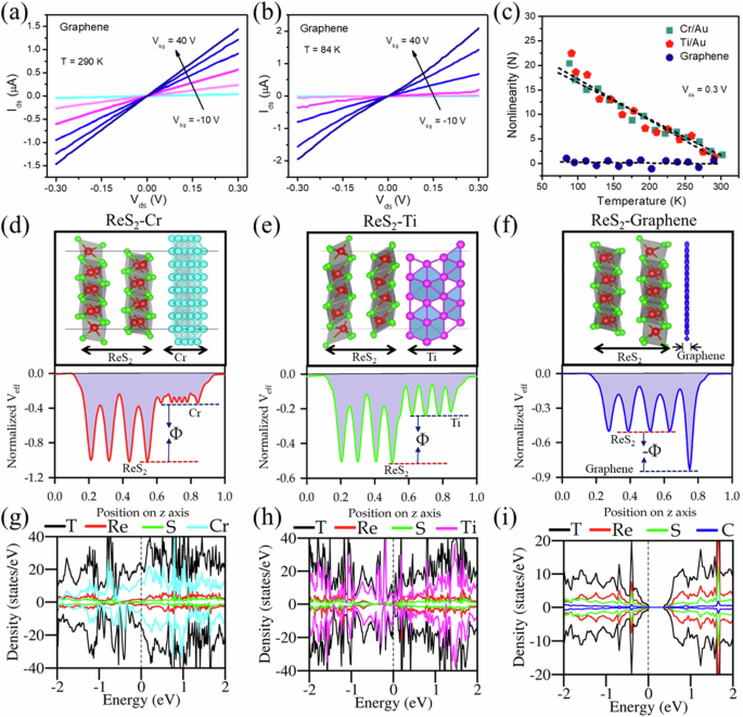
Ids-Vds characteristics of RG FET at (a) room temperature (290 K), (b) 84 K. c Nonlinearity (N) as a function of temperature for the devices. Interfacial stacking and the one-dimensional projection of the effective electrostatic potential for all three interfacial systems, (d) ReS2-Cr, (e) ReS2-Ti, and (f) ReS2-graphene respectively. Total density of states (DOS) and atom-projected DOS of (g) ReS2-Cr, (h) ReS2-Ti and (i) ReS2-graphene respectively using DFT with GGA-PBE functional in VASP.
Optoelectronic transport
To examine the impact of improved electronic behavior via contact engineering on optoelectronic performance, we systematically investigated the photodetection capabilities of ReS2 FET devices for the three types of contacts mentioned before. All the optoelectronic experiments are performed at room temperature under 633 nm light irradiation. Figure 4a depicts the transfer characteristics of a graphene-contacted ReS2 FET (RG) under different effective illumination powers (λ = 633 nm) at Vds = 1 V (for results of RTi and RCr devices, see Supplementary Fig. 13). The mechanism of photocurrent generation is represented in Fig. S14a (see Supplementary Material note 12). A monotonic increase of the drain current (Ids) is observed with the illumination intensities used throughout the window of gate voltage sweep, as indicated by the vertical shift of the transfer characteristics. Concomitantly, as light power increases, the threshold voltage (VT) shifts towards the negative direction (Supplementary Fig. 14b). The vertical shift in the transfer characterization is due to the generation of electron-hole pairs by incident photons, also known as the photoconduction or photoconductive effect51, while the horizontal shift in the transfer characteristics represents the photogating effect51. The photocurrent (Iph) was observed to exhibit a straightforward power-law relationship with incident power (PLED), expressed as Iph ∝ PLEDα, where α falls within the range of 0.3–0.4 (Supplementary Fig. 14c). The non-unity exponent arises from the intricate interplay of electron-hole generation, trapping, and recombination processes within the semiconductor52. The most important figure of merit of such photodetector devices is photoresponsivity (R)53,54, defined as the ratio of photocurrent generated (Iph) to effective illumination intensity (PLED), i.e.,
As depicted in Fig. 4b, R shows a steady rise with rising gate voltage across each light intensity level. With gate voltages adjusted from −40 V to 30 V while maintaining λ = 633 nm, PLED ~ 0.9 μW/cm2, and Vds = 1 V, R increases nearly three orders of magnitude, surging from 4.93 × 10³ A/W to 1.21 × 10⁶ A/W. The gate tunable R for RTi and RCr are represented in Supplementary Fig. 13c and d, respectively, displaying qualitatively similar behavior. Figure 4c represents the comparison of R for three devices at λ = 633 nm, Vds = 1 V, Vbg-VT ~ 10 V. Across all devices, the anticipated inverse relationship between R and PLED is evident55. Notably, RG exhibits superior photoresponse compared to the other devices, albeit following similar trends. Under identical experimental conditions, RG achieves a peak R value of 1.1 × 10⁶ A/W, while RTi and RCr attain maximum R values of 7.7 × 10⁴ A/W and 8.9 × 10³ A/W, respectively. These findings underscore that the graphene contacted devices fabricated in this study rank among the top-performing photodetector devices utilizing ReS2 layers reported to date56,57,58 (See Table-2 in Supplementary Material). Figure 4d–f depict the temporal photoresponse for the fabricated devices during one cycle of light modulation under the same experimental conditions of Vds = 1 V, Vbg = 0 V, λ = 633 nm, and PLED ~ 100 μW/cm2. The time response for the photocurrent decay is dominated by the two components which are most likely associated with the multiplicity of electron traps in the ReS2 channel from different surface states59. For RG, RTi, and RCr, the faster decay components are 220 ms, 440 ms, and 480 ms, respectively, while the slower decay components are 3.59 s, 5.44 s, and 5.69 s (Supplementary Fig. 15). In addition to R, the two most crucial parameters for assessing the detection limit of photodetectors are the noise equivalent power (NEP) and the specific detectivity (D*). NEP is mathematically defined as53,
where, SI represents the total noise spectral density encompassing 1/f noise, thermal noise, and shot noise. Similarly, the specific detectivity of a device can be defined as54,
where, A is the device area.

a Transfer characteristics (Ids-Vbg) of graphene contacted ReS2 device (RG) under different illumination power (PLED) of λ = 633 nm, Vds = 1 V. b Gate dependent photoresponsivity (R) of RG FET as a function of PLED. c Comparison of photoresponsivity of three different contacted ReS2 FETs at same experimental conditions of λ = 633 nm, Vds = 1 V, Vbg– VT ~ 10 V. Temporal photoresponse of (d) graphene contacted, (e) Ti/Au contacted, (f) Cr/Au contacted ReS2 FETs at λ = 633 nm, PLED ~ 100 μW/cm2, Vds = 1 V, Vbg = 0 V. g Comparison of 1/f noise characteristics of the fabricated devices in same experimental conditions, Vds = 1 V, Vbg-VT ~ 10 V.
The NEP and D* are assessed and compared by focusing on the predominant 1/f noise arising primarily due to the slowly varying intrinsic disorder or interfacial trapping-detrapping processes60,61,62. Given the susceptibility of these 2D devices to 1/f noise (see Supplementary Material note 14 for details), which constrains their detectivity, evaluating the level of 1/f noise is pivotal. A comparison of normalized current noise power spectral density (({S}_{I}/{I}^{2})) (at 1 Hz) for the different devices are represented in Fig. 4g. Remarkably, compared to RTi and RCr devices, the noise magnitude of RG reduces by almost two orders of magnitude, being 8.3 × 10⁻⁸ Hz−1, 7.83 × 10⁻⁶ Hz−1 and 8.70 × 10⁻⁶ Hz−1 at Vds = 1 V and Vbg-VT ~ 10 V, for RG, RTi and RCr devices, respectively. This can further be visualized from the time domain current fluctuation data (({delta I}_{{ds}}/{I}_{{ds}})) exhibiting much lower fluctuation in RG device compared to the other two (Supplementary Fig. 16a). To calculate the NEP and D* at all gate voltages, the gate dependence of noise was measured showing similar 1/f type of behavior with monotonic decrease of noise with increasing gate voltage (see Supplementary Fig. 16 for details)63. The observed noise reduction can most likely be explained by the reduced contact resistance and improved channel mobility in RG64,65. Considering the influence of 1/f noise, the calculated NEP and D* are illustrated in Supplementary Fig. 17. Results indicate that the NEP and D* for RG are 9 × 10⁻¹⁷ W/Hz0.5 and 3.2 × 10¹² Jones, respectively. Conversely, for RTi and RCr, the NEP values become 5.8 × 10⁻¹⁵ W/Hz0.5 and 1.4 × 10⁻¹⁴ W/Hz0.5, with corresponding D* values of 6.5 × 10¹⁰ Jones and 3.9 × 10¹⁰ Jones, respectively. Hence, RG clearly outperforms the other devices in terms of its exceptional weak light detection capabilities.
In summary, we have shown that the use of graphene electrodes with atomically clean interfaces can lead to a nearly barrier-free contact in ReS2 with almost ohmic nature of the conduction. This device configuration drastically lowers the contact resistance, resulting in an enhanced charge carrier mobility (~25 cm2/Vs) and an outstanding on/off current ratio exceeding 105 at room temperature. Additionally, the improved contact facilitates access to the ReS2 channel, enabling the observation of a metal-insulator transition driven by electron-phonon coupling even in a two-terminal configuration. First-principles analysis of these three interfacial systems RCr, RTi, and RG reveals the absence of MIGS in case of RG devices, which is in line with the experimental observation. We further demonstrate that superior optoelectronic performances of the graphene-contacted devices exhibiting higher photoresponsivity >106 A/W, being more than two orders of magnitude higher compared to the Ti or Cr contacted devices. More importantly, improved electronic behavior leads to a substantial reduction of low-frequency electrical noise by more than two orders of magnitude, resulting in significantly lower noise equivalent power of 9 × 10⁻¹⁷ W/Hz0.5, and a higher specific detectivity of 3.2 × 10¹² Jones at 633 nm. We believe, our approach of employing graphene as a tunable contact provides a new pathway toward contact engineering for 2D semiconductors and can enable new opportunities for future electronics and low-temperature quantum transport in 2D materials.
Experimental methods
Synthesis of ReS2 single crystal
A two-step process has been adopted for the growth of ReS2 Single crystals. High purity Re and sulfur powders were thoroughly mixed in an agate mortar and cold pressed into a pellet. This pellet was then loaded into a thick-walled quartz ampoule and sealed in a vacuum of ~10-6 Torr. The quartz ampoule was then heated in a box type furnace by slowly ramping the furnace to 1150 °C at the rate of 15 °C/hr. and held at this temperature for about 72 h. before cooling it to room temperature. This pre-reacted material was then subsequently used for the chemical vapor transport. About 1 g of the pre-reacted ReS2 powder along with I2 (150 mg) was taken in a 25 cm long quartz tube which was sealed in a vacuum of about 10−6 Torr. The quartz tube was placed in a two-zone furnace. The hot zone was maintained at 1000 °C and the cold zone was maintained at 960 °C and this gradient was maintained for about 8 days to enable the vapor transport and recrystallization of the material. Several nucleation happened and tiny flakes of ReS2 single crystals crystallized at the cold end of the crucible.
Device fabrication
Each of the 2D materials, including the graphene (supplied by SPI Supplies), layered hBN (supplied from NIMS, Japan), and few layered ReS2 flakes, are mechanically exfoliated from their bulk crystals by using scotch tape on Si/SiO2 substrate. The typical thickness of the ReS2 flakes is ~5 nm in all the fabricated devices. To ensure uniformity in the experiments, graphene, and hBN flakes are chosen to be approximately 4 nm and 14 nm thick in all devices respectively (Figs. S2 and S3). Then, the different hybrid stacks (hBN-ReS2/ hBN-ReS2-graphene) are fabricated by standard pick up and attach based dry transfer method66. The few-layered hBN is a wide band gap (approximately equal to 6 eV) semiconductor, which acts as the bottom insulating surface with fewer defects than SiO2 and also provides an atomically flat platform for ReS2 channels. The few layered graphene is put on top of ReS2 which acts as the contact electrodes. The electrical contacts are fabricated by laser writer lithography (LW405D-MICROTECH) technique followed by metallization with e-beam evaporation of Ti/Cr-Au (5–50 nm) with a well-controlled deposition rate (>0.5 Å/s) at 10−6 mbar. The channel length of all the devices are in the range of 5–7 μm. All the devices are annealed at 300 °C in the presence of Ar-H2 gas for 3 h in order to get better electrical contacts.
Materials and devices characterizations
All the exfoliated 2D materials are characterized by Raman spectroscopy (LabRam HR Evolution; HORIBA, France with 532 nm laser) and atomic force microscopy (AFM) (di INNOVA). Electrical transport measurements are performed at high vacuum (>10−5 mbar) inside a homemade cryogenic insert. A Lake Shore temperature controller (LS336) is used to control and measure the temperature. Optoelectronic experiments are carried in a homemade electronic setup having an optical window. An MFLI lock-in amplifier (Zurich Instruments), a Keithley 2450 source-meter along with a current to voltage preamplifier (Femto DLPCA-200) are used in all of the experiments with an AC two-probe configuration at a carrier frequency of 83.67 Hz. For the photocurrent measurements we used well-calibrated and collimated 633 nm LED (Thorlab) sourced by a DC2200 power supply with a spot size of ∼3 mm. The LED powers are calibrated by using a Flame-Ocean Optics spectrometer with an integrating sphere setup.
Computational methods
We have investigated its electronic properties from spin-polarized first principles density functional theory. The calculations are performed using projector augmented wave (PAW) potentials. The valence orbitals of Rhenium (Re) include 5p, 6s, and 5d, while those of Sulfur (S) comprise 3s and 3p orbitals. The exchange-correlation interactions are treated after using the generalized gradient approximation (GGA) with the Perdew-Burke-Ernzerhof (PBE) exchange-correlation functional, implemented in VASP67,68. Plane-wave cut-off energy is set as 500 eV and Monkhorst-Pack meshes 5 × 5 × 3 are used for electronic structure calculation. The van der Waals interactions are implemented by using DFT-D3 method of Grimme69.
The calculation of effective electrostatic potential and related properties are computed using QuantumATK 15.1 package as described in our earlier work70. The calculations apply double-zeta polarized basis sets with GGA-PBE exchange correlation at an electron temperature of 300 K. The DFT-D3 method is employed to incorporate the influence of nonlocal dispersive forces, such as the van der Waals interactions. A refined k-point grid of 5 × 5 × 3 was utilized, followed by a broadening of 0.1 eV.
The effective electrostatic potential is calculated by using the relation ({V}_{E}left(rright)=-frac{{V}_{H}left(rright)}{e}) and the electrostatic difference potential by ({delta V}_{E}left(rright)=-frac{delta {V}_{H}left(rright)}{e}). The Hartree potential ({V}_{H}left(rright)) is calculated from the Poisson equation as, ({{nabla }^{2}V}_{H}[n]left(rright)=-frac{{e}^{2}}{4{boldsymbol{pi }}{{rm{varepsilon }}}_{0}}n(r)), where, (nleft(rright)=delta nleft(rright)+mathop{sum }nolimits_{I}^{{N}_{{atoms}}}{n}_{I}(r)), (delta nleft(rright)) is known as electron difference density, ({n}_{I}(r)) is the compensation charge of atom I and Natoms is the number of atoms.


Responses