2D materials-based 3D integration for neuromorphic hardware

Introduction
As technology advances, there is greater demand for computing resources, which consume vast amounts of energy. Developing efficient computing technologies is critical to achieving a sustainable system1. Efficient computing requires innovation at the level of semiconductor technology and computing architecture. As complementary metal-oxide semiconductor (CMOS) technology approaches the limits set by Moore’s Law, researchers have been exploring alternatives to continue scaling down2. Currently, these efforts are focused on overcoming scaling limitations at the device design level. This led to the development of advanced transistor architectures and processes such as fin field-effect transistors(fin-FETs), gate-all-around FETs, and nanosheet FETs, which enabled increased device density and performance3,4,5. However, the miniaturization of CMOS process nodes still faces physical limitations. As the channel length of transistors shrinks to 3 nm and below, the semiconductor industry is exploring new ways to go beyond Moore’s Law with a new computing paradigm, called neuromorphic computing6.
Neuromorphic computing has emerged as an alternative to traditional computing systems. A critical issue in conventional computing systems is the bottleneck between memory and processors. The bottleneck hinders the achievement of sufficient processing speeds when exchanging vast amounts of data between memory and processors. Inspired by the human brain, neuromorphic computing integrates memory and processing units to improve speed and energy efficiency. It has been proposed that computing be memory-centric, rather than the traditional processor-centric. Thus, much more efficient computing methods, such as processing in-memory or near-memory, can be used to enable “more than Moore”. This paradigm shift addresses the limitations of conventional computers and offers promising solutions for high-performance, low-power computing7.
However, it requires a completely different design and packaging approach than traditional semiconductor design and packaging. In traditional planar two-dimensional (2D) packaging design, where functional layers are connected horizontally, the interconnections between these layers are separated by distances ranging from micrometers to millimeters. This results in parasitic resistance and capacitance, which can lead to issues such as signal delay and increased power consumption. In contrast, by stacking functional layers vertically through three-dimensional (3D) integration, the interconnect length between layers can be reduced to tens or hundreds of nanometers. This reduction enables wider bandwidths, minimizes delays, and lowers power consumption, all while significantly increasing integration density. Therefore, 3D integration has become essential to further enhance the integration density and performance of neuromorphic computing hardware.
To make this possible, the semiconductor industry has continued to research advanced packaging technologies such as through-silicon vias, wire bonding, flip-chip packaging, wafer-level packaging, fan-out, micro-bumping, and so on8,9. However, they face significant challenges in implementing them with existing CMOS material technologies. The bulk nature of silicon hinders reducing channel thickness below 4 nm while maintaining structural integrity in multi-layer architectures10. The presence of dangling bonds on the silicon interface introduces the defects, inducing increased leakage current and impaired device performance11. These surface states are particularly significant in 3D integration, where multiple interfaces exist. Overcoming these challenges requires materials that can withstand high internal stresses without failure. In addition, new material technologies and device structures beyond traditional CMOS material technologies are required to realize more suitable neuromorphic computing hardware12,13,14,15.
Two-dimensional (2D) materials have emerged as highly promising candidates, offering not only exceptional resistance to internal stress but also a range of other critical advantages. Because 2D materials are atomically thin, they offer a unique solution for neuromorphic computing hardware. Their intrinsic properties, such as a dangling bond-free structure, high mechanical strength, and superior crystallinity, make them exceptionally well-suited for 3D integration. They are also inherently flexible and maintain their electronic properties even at atomic scales, making them ideal for dense and efficient stacking in 3D architectures.
Integrating 2D materials into 3D architectures holds revolutionary potential for neuromorphic computing hardware. The unique properties of 2D materials, including their high surface area, tunable electronic characteristics, and compatibility with flexible substrates, are key to creating the dense, efficient, and scalable networks required for next-generation neuromorphic computing. This integration can dramatically enhance both the performance and energy efficiency of neuromorphic systems, positioning them as a strong alternative to conventional computing architectures.
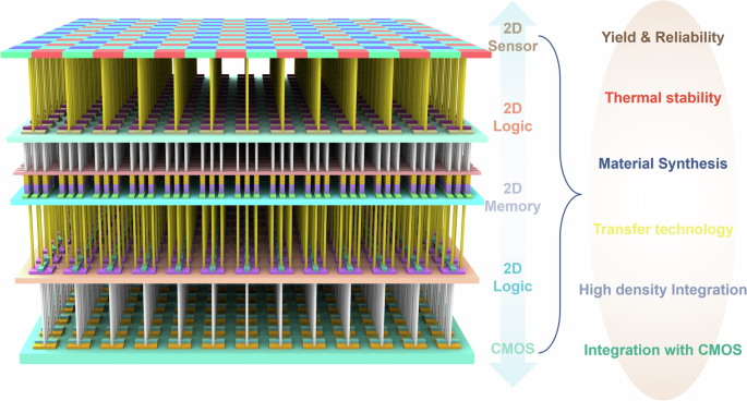
This review explores recent advances in the integration of 2D material-based neuromorphic hardware into 3D structures (Fig. 1). First, the fundamental principles of neuromorphic computing hardware are covered, and the mechanisms underlying the operation of the hardware are categorized. In addition, recent progress in the integration of 2D materials into 3D structures is systematically reviewed in terms of materials, devices, arrays, and 3D integration. Finally, the challenges facing current 2D-based neuromorphic hardware technologies integrated into 3D structures will be discussed, and some perspectives for achieving industrial-level implementations will be proposed.

A schematic of the 3D integrated neuromorphic hardware roadmap using 2D materials.
Fundamentals of 2D material-based neuromorphic hardware
Unlike traditional charge-based CMOS memory technology, neuromorphic hardware incorporates novel resistive-based memory devices such as memristors, which are two-terminal devices that combine memory and resistive functionality. Memristors operate by switching between high resistance states (HRS) and low resistance states (LRS), storing data in a non-volatile manner7,16 or diffusive manner17. These resistive switching behaviors can be used to artificially mimic the behavior of the synapses and neurons that make up the human brain. The human brain, comprising ~1015 synapses and 1011 neurons, is a highly complex and dynamic system that enables memory, cognition, and reasoning18,19.
In this chapter, we explore how 2D materials can implement resistive switching behaviors using different operation principles and what the characteristics of artificial synapses and artificial neurons as building blocks in neuromorphic computing hardware.
Operation mechanisms of 2D neuromorphic devices
Several types of 2D materials exhibit exceptional properties for memristive technology. Memristors based on 2D materials can be categorized by their operation mechanisms, which include conductive filament formation, vacancy migration, charge trapping and de-trapping, phase change, and ferroelectric polarization.
The formation of conductive filaments is the most widely recognized resistive switching mechanism. It involves a change in resistance due to the formation and rupture of metallic filaments, typically explained by the electrochemical metallization (ECM) and valence change mechanism (VCM). In ECM, metal cations from active metals like Ag form conductive filaments, thereby altering the resistance state (Fig. 2a). In VCM, anions migrate, creating vacancies that result in conductive filaments, especially when 2D materials are sandwiched between inert metals (Fig. 2b). For example, Wang et al. demonstrated robust memristors using MoS₂ sandwiched between graphene electrodes, where MoS₂ reacted with oxygen to form MoS2-xOₓ and sulfur vacancies were compensated by oxygen ions20.
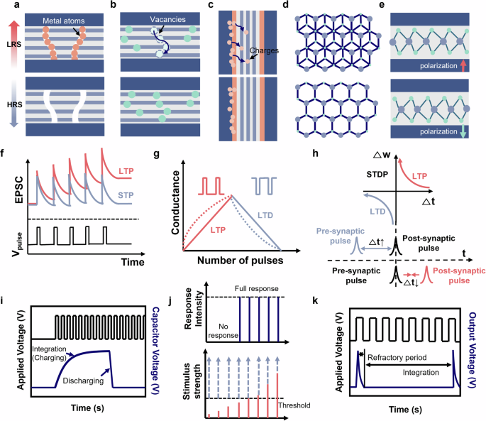
a–e Operation principles of 2D materials-based neuromorphic computing hardware: a ECM, b VCM, c Charge-trapping, d Phase-change, and e Ferroelectric polarization. f Two types of synaptic plasticity: LTP and STP. g LTP and LTD characteristics in terms of weight modulation. h STDP behavior according to synaptic pulses. i Behavior of the neuron with Leaky-Integrate-and-Fire (LIF) model. j Schematic of all-or-none law. k Refractory period and integration of neuron devices.
Charge trapping and de-trapping phenomena, another mechanism observed in 2D materials, occur within charge-trapping layers at the interfaces between 2D materials and metals, known as weight control layers or control gates (Fig. 2c). Under an external electric field, electrons tunnel and become trapped in these layers, inducing potential changes. Vu et al. fabricated a memristor array based on MoS₂ and Al₂O₃, achieving a high on/off ratio exceeding 10³ and endurance over 8000 cycles21.
The phase-change mechanism, influenced by the crystallinity of 2D materials, provides high reliability, stability, and multi-level resistance states, making it highly relevant for neuromorphic applications. Typically, 2D materials exhibit lower resistance in crystalline states and higher resistance in amorphous states, primarily controlled by heating and quenching times (Fig. 2d). For instance, MoS₂ shows local phase transitions between the semiconducting 2H phase and the metallic 1T phase22. Additionally, ion modulation under an external electric field can drive phase changes in 2D materials, as introduced by the accumulation of Li ions, which alters the phase of MoS₂ and controls synaptic behavior through ion intercalation.
Moreover, some 2D materials exhibit ferroelectricity, characterized by spontaneous electric polarization under an external bias, which is retained even after the electric field is removed, making these materials highly suitable for non-volatile memory applications such as ferroelectric random-access memory, ferroelectric FET (FeFET), and ferroelectric tunnel junction (Fig. 2e). Notably, α-In₂Se₃ is a 2D material with ferroelectric polarization, and researchers have successfully emulated synaptic plasticity using α-In₂Se₃-based FeFETs23. The polarization direction changes with applied voltage, altering the charge density. These ferroelectric switching mechanisms position 2D materials as promising candidates for neuromorphic computing architectures.
Neuromorphic hardware: artificial synapses and artificial neurons
In the human brain, electrical stimuli are collected and summed by the neuron’s cell body through synaptic connections at the dendrites. When these stimuli reach a certain threshold, the neuron generates and transmits a spike along its axon. This spike is then conveyed to other neurons via synapses, where it either strengthens or weakens the signal based on synaptic weight. The interconnected neurons form a biological neural network capable of processing vast amounts of computational functions. In these networks, information processing occurs through the flow and modulation of electrical current. Unlike digital circuits, where memory and transistor blocks perform these roles, neuromorphic systems utilize artificial synapses and neurons to achieve similar functions24.
A synapse refers to the connection between neurons and is critical for transmitting large volumes of analog information25. When a spike signal is applied, excitatory post-synaptic current is measured, indicating a temporary increase in current (Fig. 2f). In this process, the strength of signal transmission can be either strengthened or weakened, a phenomenon known as synaptic plasticity. Synaptic plasticity, including long-term potentiation (LTP) and long-term depression (LTD), is essential for analog memory systems requiring long retention times (Fig. 2g). In addition to LTP and LTD, other forms of synaptic plasticity, such as short-term potentiation (STP) and short-term depression (STD), also play significant roles. LTP and LTD involve the enhancement of synaptic weight over extended periods, while STP and STD revert to their original states more quickly26.
Moreover, synaptic plasticity is influenced by spike timing, where differences in the timing or rate of spikes between neurons can either strengthen or weaken the synaptic connection, a phenomenon known as spike-timing-dependent plasticity (STDP) and spike-rate-dependent plasticity27. When the time interval of post-synaptic or pre-synaptic pulses decreases, the synaptic weight is further strengthened; otherwise, it is weakened. In STDP, the synaptic weight typically follows an exponential function of the time interval (Fig. 2h). This synaptic modulation is crucial for information storage and processing in neuromorphic computing systems.
Early approaches to emulating the human brain involved implementing neuron models, such as the Hodgkin-Huxley and Izhikevich models, using CMOS semiconductor processes28. The simplest model, the Leaky Integrate-and-Fire (LIF) model, demonstrates how a neuron integrates charge based on signals received at the synapse and fires an action potential once the potential surpasses a threshold29 (Fig. 2i). Although this model does not replicate the diverse patterns of action potentials observed in biological neurons, it serves as an effective engineering model for computational needs in neural network structures. The LIF model is particularly valued for its simplicity and speed, making it suitable for various neural network applications30,31.
A key feature of artificial neurons is the “All-or-Nothing” law, where a neuron fires only when the stimulus exceeds a specific threshold level; otherwise, no spike is generated (Fig. 2j). Another important characteristic is the refractory period, the time during which a neuron cannot generate another spike after firing one (Fig. 2k). This refractory period ensures that signals propagate in only one direction through action potentials. By emulating artificial synapses and neurons, neuromorphic systems can replicate the advanced computational capabilities of the human brain, offering significant potential for the development of intelligent systems.
Progress of 3D integration with 2D materials
Achieving the technology to integrate 2D material-based neuromorphic computing hardware into 3D structures requires numerous design considerations. To attain large-scale integration, it is crucial to ensure excellent performance at the device level, beginning with material synthesis, and facilitate integration with various arrays for industrial-scale 3D systems. Recently, some breakthroughs have been published that make this technology possible. In this chapter, we will systematically explore them at the level of materials and devices, arrays, and 3D integration.
Material and device level
3D integration of 2D materials on Si platforms often requires transferring high-purity thin films grown on other substrates to the desired substrate. The transfer process is generally divided into polymer-assisted and metal-assisted transfer methods. In polymer-based transfer (Fig. 3a), a 2D layer is grown on the growth substrate and then coated with a polymer such as polymethyl methacrylate (PMMA). The growth substrate is removed using an etchant or mechanical exfoliation, and the 2D layer is transferred to the target substrate. The polymer is then removed using a chemical solvent32.
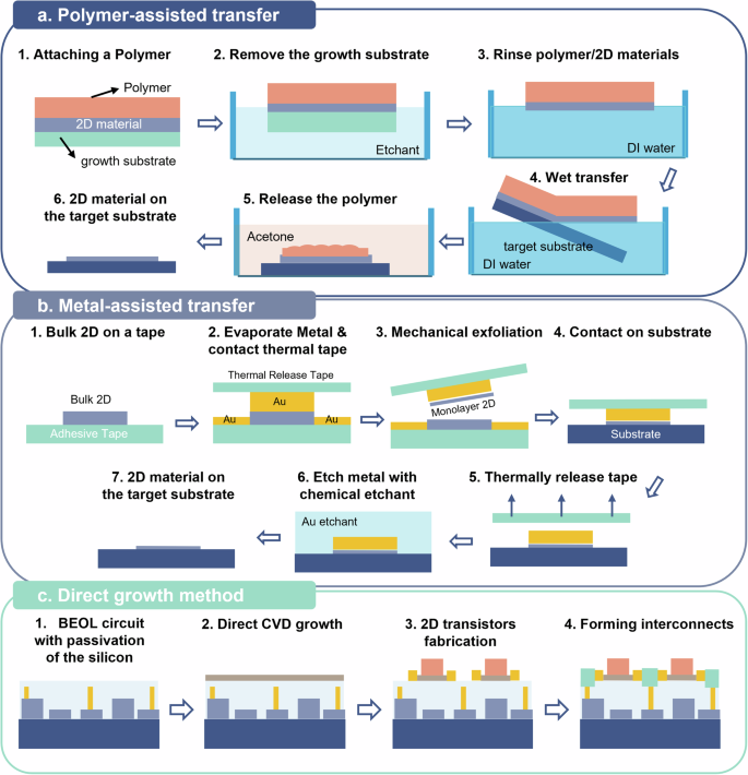
a Polymer-assisted transfer. b Metal-assisted transfer. c Direct growth method.
However, polymer-based transfer methods often suffer from low yield due to weak adhesion between the polymer and 2D materials. Metal-assisted transfer methods are gaining attention as an alternative (Fig. 3b). For instance, Au-mediated exfoliation techniques have been developed, where bulk 2D materials are coated with gold, and thermal tape is used to contact the target substrate, followed by heating33. This method achieved MoS2 monolayers over 500 µm. Additionally, Liu et al. demonstrated layer-by-layer exfoliation of 2D Van der Waals (VdW) crystals using the strong adhesion between gold and transition metal dichalcogenides (TMDs)34. Recently, Li et al. succeeded in growing wafer-scale HfSe2 using molecular beam epitaxy and transferring it with metal assistance. The use of Au in the transfer process protected the 2D film and increased yield, resulting in successful array implementation35.
In addition to exfoliation methods, techniques for growing 2D thin films directly at the desired location for large-scale synthesis are also being explored (Fig. 3c). Chemical vapor deposition (CVD) was used to successfully grow monolayer MoS2 on a SiO2 substrate at the wafer scale36. In 2015, Kang et al. achieved the growth of high-mobility MoS2 thin films on 4-inch wafers using metal-organic CVD (MOCVD), demonstrating the potential for industrial growth of TMDs by growing monolayer MoS2 on various substrates such as Al2O3, HfO2, and SiN37. While most 2D material growth methods rely on epitaxial growth requiring precise kinetic modulation, a non-epitaxial growth method was introduced for the geometrically confined growth of WSe238. Additionally, MoS2/WSe2 heterostructures have been successfully grown, showing excellent electrical performance.
2D materials offer superior electrical properties compared to silicon, which is especially beneficial in 3D integration where reducing power consumption and heat generation is critical. Scaling down the interlayer dielectric (ILD) thickness can cause significant threshold voltage (VTH) variations in FETs. However, some simulation results show that 2D materials can effectively control VTH, minimize leakage currents, and reduce the subthreshold swing. For example, when ILD thickness is reduced to 10 nm, VTH variation can increase by up to 30%39. Simulations suggest that incorporating graphene as a grounded back gate can mitigate these effects. A graphene layer as thin as 0.7 nm reduces capacitive coupling to below 1%, stabilizing VTH and improving overall device performance. This demonstrates the advantages of 2D materials in controlling electrical interference and enhancing performance in 3D structures39.
Array level
While researchers have made significant progress in implementing artificial synapses and artificial neurons at the single-device level with 2D materials40, integrating them at the array level has been hampered by technical challenges such as device-to-device uniformity, selection techniques, contact engineering, and so on. While implementing arrays with 2D neuromorphic devices is challenging because of the many factors that need to be considered, several studies have attempted to realize array-level implementation. For instance, Chen et al. reported a 10 × 10 high-density 1 R crossbar array using h-BN, achieving a 98% yield with low device-to-device variability of 5.74%41 (Fig. 4a). They used an artificial neural network model for image recognition where the classification accuracy of 98.02% was achieved. Integrate-and-fire artificial neurons in spiking neural networks (SNN) were also used by replacing the top electrode with silver. Similarly, Roldan et al. demonstrated SNN with h-BN memristors as hundreds of neurons42. They emulated STDP by applying spikes with varying time delays between pre- and post-synaptic neurons. The conductance of the memristors was measured as a function of time, and the STDP curve was plotted to show how the synaptic weights evolved based on the spike timing differences. SNN-based memristors using STDP learning showed good accuracy in image recognition, providing an efficient solution for neuromorphic computing.
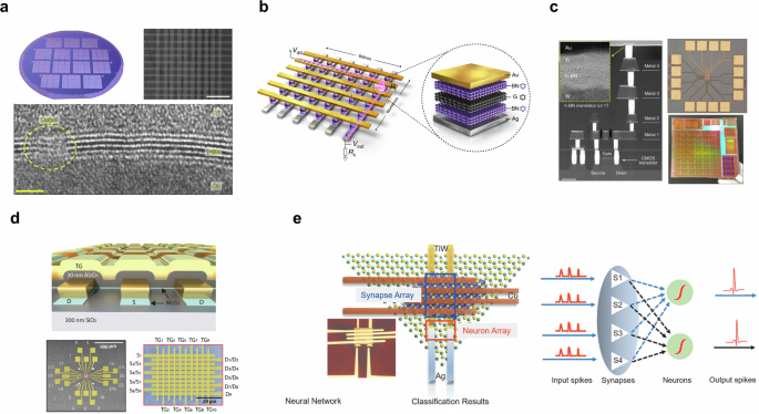
a 1 R array. Reproduced with permission41. Copyright 2020, Springer Nature. b Self-selective array. Reproduced with permission45. Copyright 2019, Springer Nature. c 1T-1R array. Reproduced with permission75. Copyright 2023, Springer Nature. d Mem-transistor array. Reproduced with permission48. Copyright 2020, John Wiley & Sons. e Neuron-synapse integrated array. Reproduced with permission50. Copyright 2020, John Wiley & Sons.
In addition, Li et al. fabricated a 5 × 5 crossbar array based on PdSe2, exhibiting synaptic plasticity43. However, the critical issue in high-density crossbar arrays with 1 R structures is the sneak path current. Without selection devices, the process of programming or reading a particular element within a crossbar causes adjacent neighboring elements to be programmed or read along with it, making accurate processing difficult. These unintended currents can activate adjacent cells, leading to decreased accuracy in both write and read operations as the array size increases, ultimately leading to increased energy consumption and reduced overall device performance44.
To address sneak path currents, many studies have focused on selective devices with memristors to build self-selective or 1T-1R (one-transistor-one-memristor) architectures. Selectors are two-terminal devices that exhibit LRS when the threshold voltage is exceeded and HRS otherwise. This feature allows selectors to mitigate sneak path currents. While the role of selective devices is marginal in smaller arrays, they are essential for large-area arrays. Sun et al. successfully implemented a self-selective memristor crossbar array with a structure of Ag/h-BN/graphene/h-BN/Au45 (Fig. 4b). The heterostructure of graphene and h-BN functioned as a selector, achieving a self-selectivity ratio of 1010 and a high conductance ratio of 103. This result demonstrates that integrating selectors can reduce crosstalk issues and enable higher levels of integration.
Transistors are also significant components for mitigating sneak path currents. As three-terminal devices, transistors switch based on the gate voltage and drain-source voltage, ensuring that only the desired devices are activated. Zhu et al. fabricated a CMOS-based 5 × 5 crossbar array with 1T-1R microchips, combining CMOS transistors with h-BN memristors, showcasing the compatibility of 2D materials with CMOS technology (Fig. 4c). Recently, Fu et al. demonstrated the homogeneous integration of transistors and memristors using MoS2, achieving a 2 × 2 array with 91% pattern recognition accuracy. The integration of 1T-1R memory cells could also address the Von Neumann bottleneck found in traditional silicon-based memory, which leads to higher integration density and reduced power consumption. Sivan et al. fabricated WSe2-based ReRAM with low switching energy as low as 2.9 pJ per bit46. It demonstrates significant energy efficiency, which is crucial for supporting fast learning and low-power operation in neuromorphic systems. However, adding components like transistors or selectors can increase the footprint. Feng et al. successfully created a 10 × 10 mem-transistor array with a cell size footprint of 3–4.5 F2 47. Unlike memristors, mem-transistors have an additional terminal for precise switching modulation. Lee et al. developed a MoS2 dual-gate mem-transistor array, which allowed for refined control of synaptic plasticity by managing the intermediate resistance state through dual gates. Linear and symmetric synaptic responses enabled the recognition rate of 94% utilizing multilayer perceptron ANN48. (Fig. 4d). Especially, most of the research in terms of crossbar array consists of simulation results by neural networks. Li et al. showed the potential of neuromorphic computing by using energy-efficient multiply-and-accumulate operations and ANN35. They successfully achieved high recognition accuracy through an HfSe2-based crossbar array. Research has explored implementing ANNs not only through memristor arrays for electrical signal processing but also using photodiode arrays. Mennel et al. introduced WS2-based neural network image sensors for machine vision49. This system presents two types of ANNs: classifiers and autoencoders, enabling rapid image processing. Unlike traditional methods that convert images to digital format for neural network processing, this method allows for real-time image sensing and processing directly on the sensor itself. Consequently, the system can classify and encode images at ultrafast speeds by the tunable photoresponsivity of 2D materials. This research proposes a high-speed, hardware-based neural network, representing a significant advancement in machine learning and real-time image recognition technologies.
In addition to implementing arrays of only artificial synapses or arrays of only artificial neurons, new array designs have been proposed in which arrays of artificial synapses and arrays of artificial neurons are interconnected to form a unified array structure. Hao et al. demonstrated an array of artificial synapses, and an array of artificial neurons connected to each other (Fig. 4e). They used MoS2 single crystals to emulate a LIF neuron model and connected it to a Cu/GeTe-based synaptic array to implement a fully memristive artificial neural network50.
3D integration level
Recently, some significant studies have been reported that go beyond planar 2D structures to achieve 3D structures by vertically stacking multiple 2D material-based functional layers. The unique properties of 2D materials, such as their mechanically stable, dangling-bond-free nature, make them ideal for vertical integration. The technology has overcome many technical limitations and is now being reported for various applications such as process-in-memory computing, near-memory & near-sensor computing, 2D logic architectures, etc. One widely known technique is monolithic 3D integration (M3D), which involves vertically stacking individual device components and integrating different chip layers on a single wafer.
Researchers have combined M3D integration with neuromorphic computing hardware to demonstrate power-efficient computing solutions. Kang et al. successfully implemented a 2D material-based neuromorphic system using M3D technology51 (Fig. 5a). This neuromorphic computing layer consists of a multi-stacked structure with WSe2/h-BN-based memristor arrays and MoS2-based transistor arrays, functioning as neuromorphic processors. The layer was monolithically integrated with sensing, signal processing, and logic layers, demonstrating the potential of 2D materials in advanced computing applications.
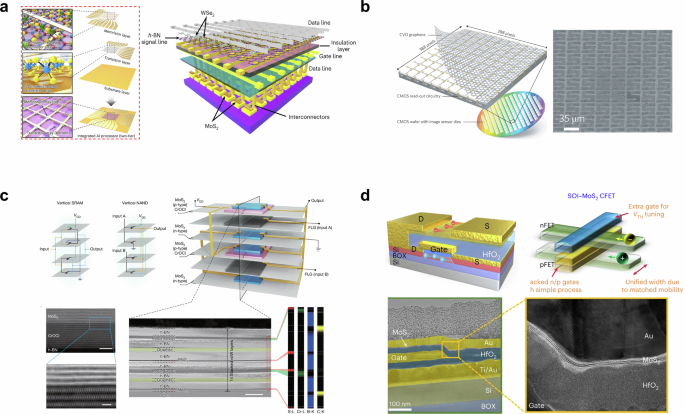
a 3D integration of all-2D-based logic, memory, and sensors. Reproduced with permission51. Copyright 2023, Springer Nature. b 3D integration of logic and sensors with CMOS circuit. Reproduced with permission53. Copyright 2017, Springer Nature. c All 2D-based 3D integration of complementary inverter. Reproduced with permission55. Copyright 2024, Springer Nature. d 3D integration of inverter based on CMOS and 2D materials. Reproduced with permission56. Copyright 2022, Springer Nature.
Recent notable advance includes the successful implementation of a 3D circuit by stacking MoS2 and WSe2-based FETs in a three-tier configuration52. The channel length of each 2D FET was scaled to 45 nm, and wafer-scale monolithic integration was achieved. In each tier, more than 10,000 devices were achieved and realized multifunctionalities such as storage, sensory, and logic. These non-computational systems could be incorporated through 3D integration and show the potential of neuromorphic and near-sensor computing.
However, most of the integrated circuits are based on CMOS, where incorporation with 2D materials is a significant issue. The potential of monolithic integration of 2D materials and CMOS circuits has been demonstrated by graphene-based image sensors. Goossens et al. integrated graphene with a CMOS imaging system to create a 388 × 288-pixel image sensor, demonstrating the progress in optoelectronics technologies through M3D integration53 (Fig. 5b). Beyond logic and memory layers, 3D integration of sensory layers also offers significantly improved energy efficiency, particularly for near-sensor applications54.
On top of that, recent efforts have focused on vertically stacking functional layers, including sensing and logic. Guo et al. demonstrated the MoS2 layer with the antiferromagnetic insulator chromium oxychloride (CrOCl) to induce strong VdW interfacial coupling55 (Fig. 5c). This enabled the differentiation into n-type and p-type through polarity engineering, forming 3D complementary logic. Consequently, they successfully implemented a 3D integration of logic circuits by vertically stacking 10 VdW layers. Similarly, Tong et al. demonstrated 3D stacked logic gates based on MoS2 and silicon56 (Fig. 5d). This was achieved using a 4-inch fabrication process, indicating the potential of integrating conventional silicon with 2D materials57,58.
The progress in 3D integration of 2D materials marks a significant advancement in the field of electronics, particularly in neuromorphic computing and optoelectronics. By leveraging the unique properties of 2D materials and the benefits of 3D architectures, researchers are paving the way for more efficient and powerful computing systems.
Challenges and perspectives for 3D integration of 2D-based neuromorphic hardware
In recent years, the technology for 3D integration of 2D materials in neuromorphic hardware has made remarkable progress and shows great potential. Integrating various functional layers such as sensors, memory, and logic in 3D on top of the CMOS circuit (Fig. 6), which were previously fabricated in 2D planar structures and connected by wires or off-chip transfers, enables much better performance in terms of processing speed, energy efficiency, and density. However, there are still a number of technical challenges in moving towards commercialization (Fig. 1). This chapter discusses the perspectives and challenges to consider for the 3D integration of 2D materials for neuromorphic computing hardware.
A schematic illustration of perspectives and challenges for integrating 2D materials-based devices into 3D structures.
Materials synthesis and transfer technologies
While there is currently a lot of intriguing research being reported on device-level implementations of neuromorphic hardware and various 2D materials, commercial-scale implementations require fabrication techniques that go beyond the single-device level. In particular, wafer-scale 2D material synthesis is essential to reach the level of 3D integration that enables higher density and energy efficiency. The ideal technology would be to synthesize uniform, high-quality 2D thin films at the desired location and on a large scale.
Various process techniques have been proposed and studied for the direct growth of 2D materials at large scale, including CVD57,58,59, chemical vapor transport60, atomic layer deposition61, and molecular beam epitaxy62. However, the limitations of the heat budget due to the high-temperature process, the inability to obtain high-quality thin films depending on the type and crystallinity of the substrate, and the difficulty of controlling the layers on an atomic scale need to be further addressed. In particular, the high-temperature conditions required by most of these processes make it difficult to reach a thermal budget compatible with CMOS. MOCVD is leading among these technologies because it has the advantage over conventional CVD of precise control of precursors, which enables layer-by-layer controlled synthesis of high-quality thin films over large areas63. However, there are still trade-offs between thermal budget and film quality, requiring an optimized engineering process.
Transfer technology, on the other hand, is still a work in progress. This is because, unlike direct growth, it can synthesize high-quality 2D thin films without the limitations of thermal budget or substrate type. Currently, the most studied transfer technique is exfoliation, but other methods such as laser-assisted64, wafer-to-wafer65, and roll-to-roll66 have also been proposed. Therefore, there are new large-scale 3D integration research possibilities utilizing these technologies.
Thermal stability
Conventional silicon-based integrated circuits are composed of metal wires and dielectrics to carry and process electrical signals. When a high electric field is applied to them, high-energy phonons are generated at specific points on the nanoscale, and heat is generated67. If this heat is not well dissipated, it will degrade the performance of the device. In conventional planar integration designs of silicon-based CMOS, the heat generated during operation is dissipated through thermal interface materials or heat sink structures to prevent device thermal degradation of the device68. However, for 3D integration, thermal management must be considered in a different way than for traditional planar integration. Because 3D integrated structures are composed of layers of different functions and stacked vertically (Fig. 6), the distance between layers is much closer. This means that heat generated at the nanoscale can affect neighboring layers more easily, which can lead to overheating.
If heat can be directed in the desired direction and dissipated through specific channels instead of flowing vertically from tier to tier, the 3D integration structure will be much more thermally stable. 2D materials have an atomic thickness and are inherently thermally anisotropic, which can be a huge advantage in 3D-integrated structures. Recently reported studies of transition metal dichalcogenide materials have shown that random interlayer rotations in MoS2 can result in a thermal anisotropy ratio of nearly 900 at room temperature69, suggesting that 2D materials have the potential to offer significant thermal management advantages for 3D integration.
In addition, graphene-related materials have also been explored as effective heat spreaders due to their large surface-volume ratio and are expected to replace traditional materials such as aluminum and copper70. Furthermore, simulations demonstrated that graphene, when embedded between dielectrics in silicon-on-insulator chips, can improve heat transfer efficiency, reducing local temperature by up to 23% compared to silicon-only systems71. For 3D chips, graphene-based heat spreaders reduce the thermal resistance by ~60%72. Beyond these material technologies, advances in thermal modeling development and characterization techniques are needed for 3D integration technologies for 2D material-based neuromorphic hardware.
Array yield and reliability
Recent research has shown impressive progress in implementing 2D material-based neuromorphic hardware at the single device level or small array level. However, to move to the commercialization level, technologies need to be developed that can be implemented at the large-area array level. This requires more complicated device design, array-scale yield, device-to-device uniformity, reliability, and so on. Typically, device-to-device variation originates from intrinsic (vacancies, grain boundaries, etc.) and extrinsic (impurities, residues, wrinkles, etc.) defects in 2D materials. However, due to the atomically thick nature of 2D materials, many defects are inevitably introduced during large-area fabrication. Because these defects are randomly distributed in 2D thin films, it is challenging to achieve uniform device performance and reliability at the large-scale array level. Therefore, controlling defect density in 2D materials is crucial to achieve low device-to-device variation and high reliability.
Recently, various methods have been investigated to control defects in 2D materials. Tang et al. successfully fabricated MoS2 memristor arrays with low device-to-device variation through a solution process-based control of sulfur vacancies73. By performing wafer-scale arrays, they demonstrated a high pattern recognition accuracy of 98.02%. In addition, high-yield 2D device arrays of more than 90% at the wafer level have been reported41,74, but more optimization processes will need to be considered for 3D integration with peripheral circuits.
Integration with CMOS and beyond CMOS
Considering the efficiency of production lines and the maturity of CMOS processes, it is impractical to replace all silicon with 2D materials in the short term. Therefore, hybrid designs combining 2D materials and silicon are being considered. Vertical integration of 2D neuromorphic hardware on top of CMOS is being considered as a practical way in the near future75. This requires consideration of layout design, optimization of process step, interconnecting CMOS and 2D devices, and synchronization between CMOS and 2D layers.
However, to move beyond Moore’s Law, it is essential to develop advanced 2D-based ICs capable of replacing conventional CMOS ICs. Achieving this goal necessitates the development of high-performance, high-yield 2D FETs and corresponding process technologies. Additionally, electrical interference shielding and contact engineering also need to be considered as different functional layers are stacked on top of each other. When 2D neuromorphic devices with atomic-scale thicknesses are fabricated into 3D integrated structures, electrical interference between tiers inevitably occurs due to the inherent nature of 2D materials that are too thin. The effects of electrostatic coupling between conductive components can cause deleterious effects such as signal delay, noise, crosstalk, and degradation. Furthermore, most 2D materials have low in-plane resistance and high out-of-plane resistance, which need to be considered when integrating76. When 2D electronics technology matures and 2D neuromorphic devices can be monolithically integrated on top of 2D-FETs at a large scale and with high yields, semiconductor technology will be able to leap into a new phase.
Although this direction of 3D integration of 2D neuromorphic hardware has many advantages, it has been limited by many technical challenges. However, the impressive results reported in recent years give us clues to break through the technical limitations. A comprehensive survey of the recently reported results of 2D neuromorphic hardware technologies at the large-area and integrated level is presented based on material, device type, synthesis, device size, array size, dynamic range, endurance, retention, and application (Supplementary Table 1). Ultimately, the future direction for 2D neuromorphic hardware integrated into 3D structures is for sensors and processors to be physically integrated into atomic-scale 3D hardware so that they can sense information inputs on their own, compute efficiently on ultra-low power processors, and output results or actuate other connected devices. This would require developing 2D thin film fabrication techniques with uniform surface area and high yields; developing advanced processes to enable monolithic stacking within thermal budgets; developing high-performance, high-reliability neuromorphic device technologies; designing new architectures to overcome the von Neumann bottleneck by replacing CMOS logic; and developing algorithms for efficient operation.
Conclusion
In this review, we have systematically explored recent advances in 3D integration of 2D neuromorphic electronics, from materials to integrated systems. The principles and neuromorphic properties of 2D material-based device physics were discussed. In addition, recent advances in the integration of 2D neuromorphic hardware into 3D have been explored in terms of materials, processes, devices, arrays, and integration techniques. Finally, the technical challenges and future perspectives for 3D integration of 2D material-based neuromorphic hardware for commercialization beyond current CMOS technology were comprehensively discussed. While many challenges and unknown principles remain, we expect that integrating 2D neuromorphic hardware into 3D structures paves the way for moving beyond Moore’s Law.


Responses