Unraveling the influence of defects in Janus MoSSe and Janus alloys MoS2(1−x)Se2x
Se2x")
Introduction
Understanding the influence of defects on the properties of materials is paramount in the field of materials science and engineering, particularly for emerging two-dimensional (2D) transition metal dichalcogenides (TMDCs)1,2,3. Among these, Janus monolayers, such as MoSSe, have garnered significant attention due to their unique structural and electronic properties arising from the controlled incorporation of different chalcogen atoms on opposite sides of the monolayer4,5,6,7,8,9,10. While the pristine form of these materials exhibits promising characteristics for various applications11,12, including (opto)electronics13,14,15 and catalysis16,17,18, the presence of defects can significantly alter their behavior, impacting their structural stability, optical response, and electrical properties19,20,21,22,23.
In this study, we aim to illuminate the intricate relationship between defects and material properties in Janus MoSSe and Janus alloy MoS2(1−x)Se2x through a comprehensive investigation including Raman spectroscopy, photoluminescence (PL) spectroscopy, and electrical characterization. By systematically probing the influence of defects on Raman spectra, we aim to unravel the structural signatures associated with different defect types and densities. Subsequently, our analysis of PL spectra seeks to demonstrate the impact of defects on the optical properties of Janus alloys, shedding light on the radiative or non-radiative nature of defect states within the optical bandgap. Moreover, we delve into the electrical properties of Janus alloys, particularly in the context of field-effect transistors (FETs), to discern the effect of defects on charge transport mechanisms and device performance. Through a combination of experimental measurements and theoretical insights, we provide a comprehensive understanding of how defects influence conductivity, mobility, and threshold voltages in Janus alloy-based FETs. By integrating structural, optical, and electrical characterization, our study aims to not only deepen our fundamental understanding of defect physics in Janus MoSSe and its alloys but also pave the way for the rational design and engineering of defect-tailored materials for advanced electronic and optoelectronic applications.
Results
In order to understand the following results and discussions one needs to understand the basics of the structural and stoichiometric options which can be fabricated during our thermal sulfurization process akin to Zhang et al.4,6. To start Fig. 1a depicts the schematic setup for the fabrication process. This includes a multi zone tube furnace, with at least two individual heat zones. In the first heat zone sulfur powder is placed within a ceramic, which is heated up to 150 °C in order to evaporate the sulfur. This sulfur gas is then transported to the second heat zone with the help of an inert carrier gas, which is pure argon gas. The second heat zone contains the samples with the base material, in our case exfoliated monolayer MoSe2 on silicon/silicon-dioxide (Si/SiO2) substrate. This zone is brought up to 800 °C to facilitate the exchange of top layer selenium atoms with the provided sulfur atoms. An optical microscopy image of a representative sample after processing can be seen in Fig. 1c.
Se2x")
a Schematic representation of the thermal sulfurization process. b Schematics of the observed structures, which vary from pristine, and highly defective MoSe2 to a partial, and complete substitution of the top-most chalcogen layer. c Optical image of an exemplary exfoliated sample after the sulfurization process. d Comparison of a Janus MoSSe monolayer Raman signature with an exfoliated layer from a bulk MoSSe alloy with the same stoichiometry (x = 0.5; S:Se = 1:1), but with a random distribution of S and Se atoms on both sides of the monolayer crystallite as indicated by the schematic. e Evolution of the Raman signature for different samples, sorted according to their photoluminescence spectra peak positions at room temperature, as shown in f.
The many different process parameters, such as temperature, sulfur concentration, and gas flow rate play important roles for the resulting monolayers stoichiometry and structure (Fig. 1b). Our analysis reveals three distinct sample types emerging from processing, depending on these factors. We start off with a monolayer of MoSe2, as depicted, henceforth termed pristine MoSe2. These pristine MoSe2 samples are thermally etched when the sulfur concentration in the process is insufficient or if the sulfur powder depletes during processing. Instead of a substitution of Se with S, the sample incorporates an increasing number of structural defects, such as Se vacancies. These samples will in the following be labeled defective MoSe2. If the process in itself works as intended, but the processing duration falls short or the sulfur concentration diminishes towards the end, we observe partial substitutions with S. This results in a deviation from the ideal 1:1 stoichiometry while maintaining an ideal structure with little to no vacancies. These substitutional defects are limited to the top-most chalcogen layer and therefore we coined these types of structures Janus alloys in order to differentiate them from the previously studied MoS2(1−x)Se2x bulk alloys24,25,26, where the sulfur and selenium distribution is fully random on both chalcogen sides. Lastly, in the ideal case, we produce Janus MoSSe samples, wherein the substitution of the top-most chalcogen layer is complete, ensuring both crystal structure and stochiometry are ideal. In the following we show that we can clearly distinguish between structural and substitutional defects.
A commercially available bulk MoS2(1−x)Se2x alloy sample with x = 0.5, i.e. a 1:1 ratio of S:Se, was exfoliated as a reference. Figure 1d illustrates clearly the effect of structure on the Raman signature in comparison to ideal Janus MoSSe. The spectrum of the bulk-like alloy shows several different modes which can be attributed to MoSe2, MoS2, and MoSSe24,25,26, while the ideal Janus MoSSe only shows only the signature for the latter. Utilizing this we can easily differentiate the random distribution of S and Se from the asymmetrical, but homogeneous distribution in Janus MoSSe.
However, not only the structural but also the stoichiometric imperfections can be visualized through Raman spectroscopy (Fig. 1e). The order in which the Raman spectra are presented from top to bottom, corresponds to the photoluminescence (PL) emission energy of the samples in Fig. 1f. The Raman spectra evolve in a way similar to previous “real-time diagnostics” for WSSe27. Interestingly, the stoichiometry changes from x = 1 (MoSe2) to x = 0.5 (MoSSe) appear to blue shift the PL’s energy from 1.56 eV to 1.68 eV at room temperature (RT), while the introduction of defects in MoSe2 yields a red shift down to 1.50 eV (Fig. 1f). The red shift of the emission for defective versus pristine crystallites is comparable to values reported previously for several other TMDCs28,29,30. Furthermore, the PL of our Janus alloy shifts similarly with stoichiometry as the bulk-like MoS2(1−x)Se2x alloy24,26, leading us to the conclusion, that the sample’s stoichiometry affects the PL in a more substantial way than its crystalline structure. These shifts of the PL as well as the correlated Raman spectra are reproducible for different samples, with only a few meV variation due to other possible differences, such as strain. This eliminates the chance of these shifts being due to accidental and uncontrollable factors, such as unintended impurities. This band gap tuning of the 2D material through partial substitution or introduction of defects can be of interest due to its versatility in future applications.
Before exploring a potential application in field-effect transistors, we aim to analyze the influences of these material imperfections in more detail. Therefore, we divided this work’s results and discussion into three main parts, which illuminate different aspects of the effect of imperfections on our material properties.
The influence of defects on Raman spectra
We start with a more detailed analysis of the Raman spectra. The Raman spectra depicting various stoichiometries of Janus alloys MoS2(1−x)Se2x are illustrated in Fig. 2a). Prominent peaks observed at 290 cm−1, at 352 cm−1 and at 442 cm−1 correspond to the Raman-active modes of pristine Janus MoSSe, the A1g, ({{rm{E}}}_{2,text{g},}^{1}), and ({{rm{A}}}_{1,text{g},}^{2}) mode, respectively. These peak positions are consistent with prior theoretical predictions15,18,31 and experimental findings4,5,6. Additional peaks can be observed, such as the A1g mode at 240 cm−1, the D1 at 252 cm−1, and D2 mode at 263 cm−1. In Fig. 2a D1 and D2 are summarized as Di due to their proximity. These modes offer valuable insights into the structural characteristics of the material. For example, the presence of the peak at 240 cm−1 suggests the existence of pristine MoSe232 in our flake, as can be expected from our samples, which are fabricated from MoSe2 as the base material6. Furthermore, the two additional Raman modes D1 and D2 exhibit characteristics indicative of defect-related phenomena, as will be discussed in detail below. For the complete set of Raman spectra of the analyzed samples, see Supplementary Fig. 1.

a Three detailed Raman spectra from samples with different stoichiometries of S:Se. Varying from the very top, a partial substitution of the top-most selenium layer with sulfur with some remaining MoSe2, to a complete substitution at the bottom. The insets show the asymmetry of the A1g mode of MoSSe, as depicted by the two Voigt fits A and A*. b Evolution of the A* and A intensities of different samples with different stoichiometries. c Asymmetry ratio A*/A plotted against the A-exciton energy of the corresponding photoluminescence peak. d Estimated intrinsic charge carrier concentration of the samples in correlation with the asymmetry ratio. e Polarization dependent Raman spectra of a Janus alloy. f–j show the polarization dependence of A, A*, ({{rm{E}}}_{2,text{g},}^{1}), D1 and D2, respectively. Orientation is normalized in relation to the silicon peak intensity.
Another indicator for defects and other imperfections in the lattice is the line shape of the Raman modes. Something often overlooked in the literature. We find the asymmetry of the MoSSe A1g mode to be a reliable indicator of the materials’ stoichiometry. Figure 2a (insets) reveal the secondary component A* to the A1g peak, necessitating a comprehensive fitting approach. This lower wave number tail of the A1g mode of MoSSe is attributable to either charge carrier’s interaction with the phonons involved in the Raman scattering (so-called Fano effect)33 or due to quantum confinement of the sample34. A spatial confinement will constitute q ≠ 0 phonons to contribute to the scattering, causing an asymmetric line broadening, which has been observed in 2D materials35. Imperfections in the lattice will cause a higher confinement for the phonons and a stronger asymmetry. The Fano effect, on the other hand, will cause an asymmetric tail depending on the intrinsic charge carrier concentration, with a lower-wavenumber tail indicating an n-type intrinsic doping36,37. Therefore, the asymmetry of the Raman mode will depend on the free charge carrier concentration in the material. In order to assess the role of lattice imperfections on the asymmetry of the A1g mode of Janus MoSSe, we introduce a new, quantifiable factor, the asymmetry ratio A*/A. We observe a decrease in A*/A for spectra closer to x = 0.5 (Fig. 2b, c). This agrees well with the previous inference that the asymmetry is indicative of lattice imperfections in the material, as the Janus alloys with just a partial substitution will exhibit more compared to a ideal sample.
These lattice imperfection can further alter the materials’ properties, such as strain and intrinsic doping. As previously demonstrated, both strain and charge carrier concentration of a Janus MoSSe monolayers can be inferred through theoretical calculations of its Raman mode shifts6. For the graphical evaluation of the samples’ Raman mode shifts and how they manifest in strain values, and the shifts in charge carrier concentration presented in Fig. 2d, see Supplementary Fig. 2. Our examination of both Janus alloy and ideal Janus samples reveals negligible strain from the theoretical Raman mode shifts, attributed to an improved preparation technique in comparison to our earlier work, that mitigates strain induced by exfoliation6. Comparing our Raman shifts with the theoretical predictions, we observe a decrease in electron concentration for stoichiometries with x increasing towards x = 0.5 (Fig. 2d). Notably, the Janus alloy sample with the highest asymmetry ratio of the A1g mode exhibits a maximum electron concentration of approximately 1.4 × 1013 cm−2. In contrast, our ideal Janus monolayer displays an electron concentration of around 1.0 × 1013 cm−2, resulting in a relative decrease in charge carrier concentration of 0.4 × 1013 cm−2. This means an increase of the charge carrier concentration with respect to the ideal Janus MoSSe by 40%. This trend aligns with theoretical predictions regarding the work function of MoSSe, which is anticipated to be higher than that of MoSe2. Specifically, monolayer MoSe2 exhibits a predicted work function of 4.7 eV38 and a measured value of 4.3 eV39, whereas monolayer MoSSe is predicted to range between 5.13 and 5.24 eV19,40,41, representing a significant increase of roughly 20%. Thus, the monolayer MoSSe should exhibit less intrinsic doping than MoSe2 and a lower charge carrier concentration. This trend aligns well with a reduction of the asymmetry due to less free charge carriers contribution to the Fano effect.
Compared to our previous report, utilizing the theoretical strain and intrinsic doping induced Raman shifts, we find a remarkable consistency in the anticipated charge carrier concentration. There, we reported an electron concentration in the monolayer Janus MoSSe of 1.18 × 1013 cm−2 6, ultimately being somewhat larger than what we report here. However, as the flakes reported in this work exhibit negligible compressive strain compared to the previous report, the difference can be attributed to strain-induced doping6. Additionally, the influence of sulfur vacancies in MoS2 leading to increased numbers of free charge carriers is well-documented42,43,44,45. A similar behavior of sulfur vacancies in Janus MoSSe is feasible due to the same electron capturing effect of sulfur in the Janus monolayer. Therefore, a decreased level of sulfur vacancies in this work’s ideal Janus MoSSe samples compared to the previous report may contribute to the slightly reduced charge carrier concentration6.
Accordingly, we anticipate the ideal Janus MoSSe sample to exhibit the lowest defect density compared to the Janus alloys. And indeed, this is consistent with the observed trend from the theoretical predictions as shown in Supplementary Fig. 2 and Fig. 2d and the previous inference from the decreased asymmetry ratio (see Fig. 2c) indicating less phonon scattering sites.
Various scattering sites within the material, such as vacancies and substitutional defects, can also give rise to distinct Raman signatures. We report this to be the case for the two observed defect related modes D1 and D2. Utilizing polarization-dependent Raman spectroscopy (Fig. 2e), we discern the nature of these D modes. By isolating the Raman modes and plotting their intensity against the polarization angle, we differentiate between in-plane (E) and out-of-plane (A) modes, as their dependencies are given by their Raman tensors and the setup’s back-scattering geometry46. The A1g mode (Fig. 2f) exhibits intensity maxima at parallel-polarization and minima at cross polarization, while the ({{rm{E}}}_{2,text{g},}^{1}) mode (Fig. 2h) remains independent of the polarization angle, as anticipated47. Intriguingly, both D modes (Fig. 2i, j) manifest as out-of-plane vibrations. We specifically attribute the D1 mode to selenium vacancies in MoSe2, as indicated by its appearance only in conjunction with the A1g mode of MoSe2, and its Raman shift (~ 250 cm−1) consistent with prior research48,49. The observed blue shift in this phonon mode, contrasting with the red shift of MoSe2’s A1g mode at higher defect densities, agrees well with previous investigations, too48,49. Conversely, the D2 mode is exclusively observed in samples exhibiting a substantial MoSSe signal, suggesting its association with defects in Janus MoSSe. Theoretical analysis by Mehdipour and Kratzer supports this inference, proposing the D2 mode as a Raman-active out-of-plane phonon mode (at 260 cm−1) arising from a substitutional selenium atom at a sulfur site within the MoSSe lattice31.
The influence of defects on PL spectra
Given our prior discussion indicating the higher defect density in our Janus alloy samples, in contrast to the Janus MoSSe, we seek to compare their PL spectra with those of samples exhibiting even higher defect densities. By conducting power dependent PL measurements at room temperature (see Supplementary Fig. 3) and 77 K, we determine the excitonic nature of the emission, by plotting total intensity against excitation power. Figure 3 provides a qualitative juxtaposition of the photoluminescence characteristics between highly defective MoSe2 (top row), a representative Janus alloy (middle row), and Janus MoSSe (bottom row). It’s important to note that the specified powers represent the actual power at the sample, taking into account the reduction caused by the laser traversing the optical setup and the glass of the vacuum stage. The relationship between intensity (I) and excitation power (P) follows a power law:
where k characterizes the exponent of the power dependence. This exponent k can range between 0 and 2. A sublinear dependence (0 < k < 1) indicates a localized exciton (XL), a linear dependence (k = 1) signifies a free exciton (X), while an above-linear, nearly quadratic dependence (1 < k < 2) usually suggests the formation of multi-exciton processes, such as biexcitons or two-photon absorption50. However, especially in highly defective materials, a superlinear dependence can also be associated with the saturation of non-radiative recombination centers51,52.

Top row a–d: Defective MoSe2. Middle row e–h: Janus alloy. Bottom row i-l: ideal Janus MoSSe. a, e, i Power series of the photoluminescence at 77 K in 5 × 10⁻³ mbar. b, f, j Evaluation of total intensity change according to power law. c, g, k Temperature dependent shifts of the PL. d, h, l Peak position and FWHM plotted against temperature and fitted according to Bose-Einstein model.
In Fig. 3a, we show the power dependence of highly defective MoSe2. Notably, there is a discernible shift in the position of the peak. The total intensity of the PL, if the energy shift is ignored, shows a power dependence of k = 1.35 (see Supplementary Fig. 4). This superlinear dependence is likely due to the saturation of non-radiative recombination centers, which are abundant in highly defective MoSe2. At low excitation powers, excitons are efficiently captured by these defect states, leading to reduced PL intensity. However, as the excitation power increases, these defect states become saturated and can no longer capture additional excitons. This results in an increased fraction of excitons undergoing radiative recombination, causing the observed superlinear increase in PL intensity. To capture the redshift of the PL adequately, we fit the data with two Gaussian functions. At lower excitation powers, the PL’s maximum is at approximately 1.62 eV and is predominantly governed by the first Gaussian, while at higher excitation powers, the peak shifts to 1.60 eV, with the second Gaussian contributing the most. Plotting the intensity of these two Gaussians against excitation power (Fig. 3b), we observe a sub-linear dependence for the first Gaussian (in red) and a superlinear dependence for the second Gaussian (in black). This suggests the presence of a localized exciton at the higher spectral energy and the increasing influence of radiative recombination as non-radiative centers saturate at the lower spectral energy. The localized exciton is an electron-hole pair bound to lattice imperfections, such as Se vacancies, which are expected to be abundant, given the prominent D1 mode in the Raman signature (see Supplementary Fig. 5). While biexciton formation is typically associated with a quadratic dependence, and has been observed in many 2D materials53,54,55,56, in this highly defective system, the saturation of non-radiative centers provides a more plausible explanation for the observed superlinear behavior. Still, the energy difference between the states, approximately 18.68 meV, aligns well with the biexciton binding energy according to theoretical values53,57 and experimental results for monolayer MoSe256. However, for a more thorough investigation, even lower temperatures would be a prerequisite, and therefore we refrain from a more detailed discussion of this phenomenon at this stage.
In contrast, the power series analysis of Janus alloy and Janus MoSSe samples exhibits a typical excitonic behavior, featuring two distinct transitions at 1.65 eV (A) and at 1.85 eV (B) (Fig. 3e) and 1.72 eV (A) and 1.95 eV (B) (Fig. 3i), respectively. The two distinct transitions arise due to the spin-orbit coupling effect in the band structure, as anticipated for most TMDCs32. The power-dependent intensities of these peaks further support this observation, with both A and B being governed by free excitons characterized by k ≈ 1 (Fig. 3f, j). This comparison vividly illustrates that while both defective MoSe2 and Janus alloys exhibit indications of Se vacancies through the presence of the D1 mode in their Raman spectra, the PL behavior of the Janus alloy remains unaffected by these vacancies, unlike highly defective MoSe2. This discrepancy leads us to speculate that the defect states associated with Se vacancies in the bandgap of MoSe2 may either not be accessible or are no longer radiative in nature within the shifted band gap structure of the Janus alloy. It’s plausible that these defect states in the Janus alloy lie deeper within the bandgap, making them less likely to be accessed through electron-phonon interactions.
The strength of the electron-phonon interaction can be accessed through the temperature dependence of the PL. The extent of the PL’s energy shift from room temperature to lower temperatures reflects the degree of interaction between excitons and lattice vibrations facilitated by temperature. This relationship can be quantified using the Bose-Einstein statistical factors to describe the temperature depending energy shift E(T) as follows:
where E0 represents the exciton energy at 0 K, aB denotes the exciton-phonon coupling strength, and ΘE signifies the average phonon temperature58,59. Although this equation technically describes the temperature-dependent band-gap shift of a semiconductor, due to its consideration of the interaction of charge states with phonons, it is commonly employed to describe the temperature shift of the PL as well60,61. Similarly, the full width at half maximum (FWHM) of the emission peak, denoted as Γ, also depends on temperature and typically decreases at lower temperatures. This temperature dependence of Γ(T) can also be characterized by the Bose-Einstein statistical factors
Here, Γ0 represents the approximate FWHM at 0 K, Γ1 is a fictitious broadening factor arising from the model’s approximations, and ΘE is again the average phonon temperature58,59. For fitting purposes, ΘE is kept at the same value as in equation (2).
The temperature dependence of defective MoSe2 (Fig. 3c) illustrates a nominal shift in PL emission from 1.541 eV at RT to 1.595 eV at 77 K. The corresponding temperature dependence of the peak’s spectral position and FWHM are depicted in Fig. 3d. The fitting parameters suggest a relatively high average phonon temperature of 639 K, an exciton-phonon coupling strength of 294 meV, and predict an exciton emission at 0 K at 1.597 eV with a FWHM of 82.51 meV. Comparison with the Janus alloy’s temperature-dependent PL shift (Fig. 3g) reveals that the spectral shift is approximately half as strong as that of defective MoSe2, from 1.617 eV at RT to 1.645 eV at 77 K. Again, the spectral shift of exciton emission and the temperature dependence of its FWHM are plotted (Fig. 3h). The fitting parameters indicate a lower phonon temperature of 354 K and a weaker exciton-phonon coupling of 16.6 meV. The predicted 0 K emission peaks at 1.641 eV with a FWHM of 61.57 meV.
Lastly, a comparison of the two sample types with the ideal Janus MoSSe monolayer sample, shows a PL emission shift from 1.702 eV at RT up to 1.756 eV at 77 K (Fig. 3k). This spectral shift is stronger than that of the Janus alloy sample and the same as the defective MoSe2’s. The spectral and FWHM shifts are plotted in Fig. 3l. The fits reveal, that by extrapolation, the PL peak should reach an energy of 1.797 eV and a FWHM of 15.17 meV at 0 K. Furthermore, the sample’s average phonon temperature is 238 K and has an exciton-phonon coupling strength of 39.3 meV. These values for the Janus alloy and ideal Janus MoSSe are in good agreement with other TMDCs60,61. Direct comparison underscores that the ideal Janus and the Janus alloy exhibit similarly strong exciton-phonon coupling. Interestingly, the coupling is strongest by far for defective MoSe2, emphasizing the significance of defects in MoSe2 in contrast to the Janus MoSSe and Janus alloy samples.
We conclude that the strong exciton-phonon coupling in MoSe2 is due to localized excitons at defect sites, facilitating a highly probable and strong interaction. Overall, the analysis of both power and temperature dependent PL spectra confirms that the blue shift observed from MoSe2 to Janus MoSSe is primarily due to the evolution of the bandgap. In contrast, the red shift in defective MoSe2 samples is likely attributed to defect-dominated recombination.
The influence of defects on electrical properties
Having identified the presence of defects in our Janus alloy samples, which are not observed in ideal Janus MoSSe samples, we aim to utilize our findings in the context of an important application example. Specifically, we use 2D field-effect transistors (FETs), where defects play a pivotal role and defect engineering can be used to improve their performance20,21. For the Raman and PL spectra of the specific FETs shown in this work, see Supplementary Fig. 6. Figure 4a shows an optical image of a monolayer Janus alloy on a silicon/silicon-dioxide substrate, featuring two gold/chrome (Au/Cr) contacts positioned on the left and right sides of the flake. These contacts serve as the drain and source of the device, as schematically depicted in Fig. 4b. The drain-source voltage (VDS) is applied between these contacts to control the current flow (IDS) in our monolayer sample. The p-doped silicon on the device’s backside functions as our gate contact, while the 285 nm SiO2 layer acts as the dielectric medium. By applying a gate-source voltage (VGS) between the source contact and the gate, we can tune the intrinsic doping level by shifting the Fermi level. For FETs, two characteristic curves are essential: the output curve (Fig. 4c), where VGS is held constant while IDS(VDS) is measured, and the transfer curve (Fig. 4d), where VDS is constant while IDS(VGS) is measured. These curves provide insights into various properties, including contact type, conductivity (σ), mobility (μ), and threshold voltage (Vth)62. Figure 4c displays six output curves on a half-logarithmic scale, including three Janus MoSSe (blue) and three Janus alloy (purple) output curves for VGS = 0 V, 20 V, and 50 V, respectively. The asymmetry in these curves and the saturation-like behavior in the linear Plots (see Supplementary Fig. 7) observed in the Janus alloy indicates a Schottky contact, whereas Janus MoSSe exhibits a more symmetrical and more linear behavior, suggesting a more Ohmic contact. Recent theoretical predictions suggest that the intrinsic dipole of Janus MoSSe facilitates an Ohmic contact to various metals63,64. Important for the interface dipole to form, the metal in contact with the MoSSe must have a sufficiently low work function, like titanium64. Given chromium’s comparable work function (4.5 eV) to titanium’s (4.3 eV)65, we anticipate this to be the case for our contacts as well. This observation implies that our Janus sample demonstrates a relatively uniform out-of-plane dipole moment compared to the Janus alloy, which lacks stoichiometry. However, this can also be due to the different work functions of the Janus alloy and the Janus MoSSe aligning differently with the contacts’, therefore modifying the Fermi-level pinning66,67. Notably, an increased VGS appears to influence the contact type of the Janus alloy, transitioning from a clearly Schottky contact (VGS = 0 V) to increasingly Ohmic behavior (VGS = 50 V) in the half logarithmic scale. This phenomenon may result from the concurrent gating of the contact and channel regions through the global back gate employed in our FET structure. Schottky contacts can exhibit Ohmic characteristics due to the enhancement of the tunneling component at the source junction62,68.
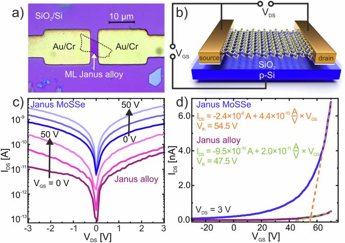
a Representative optical image of a FET fabricated from a monolayer Janus alloy on Si/SiO2 substrate. b Schematic setup of the MoSSe FET indicating the applied biases VDS, VGS. c Output characteristics on a semi-logarithmic scale of a Janus MoSSe (blue) and a Janus alloy (purple) FET with varying VGS biases. d Transfer characteristics of a Janus MoSSe (blue) and a Janus alloy (purple) FET at VDS = 3 V. Linear fit at the slopes’ maxima result in the threshold voltage Vth for Janus MoSSe (orange) and Janus alloy (green), respectively.
The conductivity σ of a 2D material can be determined from the linear relation of IDS(VDS) for small VDS. There, the device resistivity can be expressed as RD = VDS/IDS. Therefore, we obtain the conductivity of the device by
with the channel’s dimensions: L length, and W width. These dimensions were estimated from optical images of the samples. Therefore, σ can be determined in the range of (2.1−8.6) × 10−10 S for the Janus MoSSe FET and (0.37−4.9) × 10−11 S for the Janus alloy FET. We observe an increased conductivity by an order of magnitude for ideal Janus MoSSe device compared to the Janus alloy. It is important to mention that, as our setup consists of a 2-point probe measurement,we cannot separate the influence of the contact resistance on the overall conductivity of our devices. The contact resistance depends on the microscopic nature of the metal/semiconductor contact and for 2D materials the Schottky barrier between the two materials has a big impact on the contact resistance69,70,71,72,73,74. The Schottky barrier itself depends on the work functions of the two materials forming the contact and is especially in 2D material devices heavily influenced by the Fermi level pinning because of mid-gap states in the 2D material74,75,76,77. Therefore, the extracted values for the conductivity are not the intrinsic values of the 2D channel, but rather device parameters. Thus, our values are lower boundaries, and the true intrinsic values should exceed them. Nonetheless, the reduced conductivity of the alloy device is consistent with the physical picture that the alloy device is much more defective than the Janus MoSSe, resulting in more scattering sites. Figure 4d shows the transfer curves of the Janus MoSSe (blue) and the Janus alloy (purple) samples at VDS = 3 V. Here, we can clearly see the typical n-type semiconductor behavior of the FETs, supporting the previous theoretical evaluation of the Raman mode shifts, which indicated n-type doping behavior, as previously predicted6. The transfer curve of a ideal Janus MoSSe FET shows a much higher current IDS (up to ≃ 2.5 orders of magnitude), indicating better device quality due to fewer scattering sites for the charge carriers. By fitting a linear function to the steepest slope in the transfer characteristic, we can evaluate the devices’ transconductance ({g}_{m}={left.frac{partial {I}_{{rm{DS}}}}{partial {V}_{{rm{GS}}}}rightvert }_{{V}_{{rm{DS}}}}), and its threshold voltage Vth. The fits are shown in orange and green, for the ideal Janus MoSSe FET and the Janus alloy FET, respectively. The devices’ transconductance is evaluated to be 4.4 × 10⁻¹⁰ A V−1 and 2.0 × 10⁻¹¹ A V−1, respectively. Therefore, the Janus’ device transconductance is one order larger than the Janus alloy’s. In turn, we can calculate the field-effect mobility (μFE) of our device as:
where Cox is the oxide’s capacitance, we use Cox = 12.12 nF cm−2 for 285 nm SiO2. We find device mobilities of 2.42 × 10⁻³ cm2 V−1 s−1 for the Janus MoSSe FET, which is comparable to similar MoSSe FETs4, and 0.110 × 10⁻³ cm2 V−1 s−1 for the Janus alloy FET. This means, the device mobility of the Janus alloy is just about 4.5% of the Janus’ device mobility. Due to the 2-point measurement and the outputs’ linearity these values represent a lower limit for the intrinsic material mobility78. This drastically lowered device mobility indicates the presence of many scattering centers. As we have previously established, these can be due to Se vacancies, but are more likely due to the inhomogeneous nature of the Janus alloy’s sulfur and selenium distribution. Still, the mobility values even for the ideal Janus MoSSe FET are several orders of magnitude smaller than those of other TMDC FETs like MoS279,80,81 and MoSe282,83,84, as the asymmetrical nature of the material itself is detrimental for charge carrier dynamics. It has been shown though, that in principle, higher charge carrier mobilities for Janus MoSSe FETs can be achieved through additional preparation steps85.
The threshold voltages are calculated to be 54.5 V and 47.5 V, for the ideal Janus and the Janus alloy, respectively. With these Vth we can calculate the gate-induced charge carrier concentration according to
with e being the elemental charge. Equation (6) assumes a channel-dominated device which requires VGS > Vth. We calculate a charge carrier density for VGS = 70 V to be nJanus = 1.17 × 1012 cm−2 and nalloy = 1.70 × 1012 cm−2, and the difference between the Janus MoSSe and the Janus alloy to be Δn = nalloy − nJanus = 5.30 × 1011 cm−2. This means an increase of the charge carrier concentration from the ideal Janus MoSSe by 48%. Again, due to the device architecture, the values for the threshold voltage appear overestimated and in turn the gate-induced doping will be underestimated due to the influence of the contact resistance78. This could explain the disparity between the predicted intrinsic charge carrier concentrations and the gate-induced one, which is within an order of magnitude. However, the relative change in charge carrier concentration remains consistent with the theoretical evaluation of the intrinsic doping level (40%) (Fig. 2d). This evidently shows that the Janus alloy is indeed more n-doped than the ideal Janus MoSSe and that we can predict such a trend from Raman signatures’ shift alone, without the need to fabricate a time-consuming FET structure. Further, it supports our the assessment that the Fano effect leads to the asymmetry of the A1g Raman mode of Janus MoSSe.
Discussion
In conclusion, our study shows the influence of imperfections on the structural, optical, and electrical properties of Janus MoSSe and Janus alloy MoS2(1−x)Se2x. Through a comprehensive Raman spectroscopy analysis, we deciphered the intricate interplay between defects and phonon scattering, unveiling the significance of the asymmetry in the A1g mode as an easy-to-use measure of defect density. The emergence of distinct defect-related Raman modes (D1 and D2) provided further insights into the nature of defects, with D1 being associated with selenium vacancies in MoSe2 and D2 being linked to intrinsic substitutional defects in otherwise ideal Janus MoSSe. Examining the photoluminescence characteristics, we observed contrasting behaviors between highly defective MoSe2 and Janus alloys, with the latter displaying a more typical excitonic behavior despite the presence of defects. This discrepancy hints at a shifted band gap structure in Janus alloys, rendering certain defect states less accessible or non-radiative. Furthermore, our investigation of the electrical properties underscored the profound impact of defects on charge carrier mobility and device performance. The observed different contact types, from Schottky to Ohmic behavior, in Janus alloys and ideal Janus MoSSe, can be indicative of the intrinsic dipole moment in the Janus monolayer. Moreover, ideal Janus MoSSe exhibited superior conductivity and mobility compared to Janus alloys, attributed to a reduced defect density. However, we also found those defects to cause a higher charge carrier concentration in the Janus alloys compared to the Janus MoSSe, pointing towards a delicate balance between the amount of free charge carriers available for the electronic transport and the scattering of those charge carriers at the imperfections. Lastly, we demonstrated the validity of utilizing the theoretically calculated Raman shifts to assess strain and doping by showing that n-doping decreases with stoichiometry towards x = 0.5 as predicted.
Overall, our findings shed light on the relationship between structural and substitutional defects and material properties in Janus MoSSe and Janus alloys, offering valuable insights for future research and practical applications in electronic devices. To harness the full potential of these materials, further exploration into defect engineering and mitigation strategies is warranted.
Methods
Sample fabrication
Our sample fabrication starts with mechanically exfoliated MoSe2 monolayers prepared onto a silicon substrate (resistivity 0.001–0.005 Ωcm) with a 285 nm oxide layer. The substrate is cleaned in an ultrasonic bath and then treated by plasma etching (0.8 mbar ambient pressure, 80% of max. power, 10 min, Diener electronic Femto) to minimize strain. Samples are then placed inside a multi zone tube furnace (ThermConcept ROK 70/750/12-3z) approx. 25 cm downstream of 85 mg sulfur powder (Sigma-Aldrich, 99.98%). The furnace chamber is evacuated before starting the process with pure argon gas (99.9% Ar, 15 min 200 sccm). For the sulfurization process the flow is reduced to 75 sccm. The second temperature zone with the samples is heated up to 800 °C and with a delay of 9 min the sulfur follows up to 150 °C. Both temperature zones are kept constant for 20 min before rapidly cooling the oven down to room temperature. For more details see6.
The commercially bought bulk MoSSe alloy sample (2D semiconductors) was exfoliated onto a silicon/silicon-dioxide (285 nm oxide layer). Stoichiometry of x = 0.5 and high purity was tested and confirmed by the vendor.
Raman and photoluminescence spectroscopy
A WITec alpha300 RA confocal Raman spectrometer was used for both Raman and PL measurements. All measurements were done with a green laser (λ = 532 nm) with an output power of 0.5 mW, unless specified otherwise. Grid sizes were switched between 300 l mm−1 for PL and mappings and the 1800 l mm−1 grid for single spectra measurements. The low temperature PL measurements were made possible by installing a Linkam Stage THMS350EV extension temperature control system to our Raman spectrometer. The correction for the true excitation intensity for the power series was measured by a power meter through the glass of the Linkam Stage. For clearity the PL spectra at RT were smoothed by a Loess filter (0.1 strength) in Origin. It was strictly noted that there is no loss of information through this process.
Device fabrication and characterization
Through investigation with optical microscopy, suitable flakes were identified. Following a standard photolithography procedure using a maskless optical lithography machine SMART PRINT UV from microlight3D, 10 nm of Cr and 100 nm of Au were deposited through electron-beam (Cr) and thermal evaporation (Au) at a process pressure of 1 × 10⁻⁵ mbar to establish electrical contacts with the flakes.
Electrical characterization of the devices was performed with a non-commercial vacuum stage connected to a Keithley 2612B source-measure-unit. All electrical measurements in this work are performed under a vacuum of 1 × 10⁻⁵ mbar.
Usage of large language models
During the preparation of this work the authors utilized ChatGPT 3.5 (OpenAI) and DeepL in order to cross-check language and grammar. After using these tools, all authors reviewed and edited the content as needed and take full responsibility for the content of the publication.


Responses