High-throughput synthesis of high-entropy alloys via parallelized electric field assisted sintering

Introduction
Whether considering the aerospace, energy, or industrial sectors, the efficiency and reliability of engineering processes are primarily limited by the materials used in the construction of the systems employed. Properties such as mechanical strength, chemical reactivity, corrosion resistance, irradiation resistance, and melting point, often must be balanced with practical concerns such as weight and cost. Unfortunately, designing and testing new materials is often a time-consuming and cost-prohibitive process that may be unfruitful in the near term, which incentivizes companies and other entities to continue using materials that may not be optimal for their processes but which have long histories of use in similar operating conditions; consider the ubiquity of ferritic, martensitic, and austenitic stainless steels which were first developed and commercialized over a century ago and have undergone only modest changes in chemistry since their inception1. Adding to the challenges and costs associated with materials discovery and design is the number of potential alloy compositions and material combinations. With the direction of current research shifting to more compositionally complex materials, such as high-entropy alloys (HEAs), there is a nearly innumerable range of possible alloy compositions before even considering multi-material composites.
To overcome the impediments of materials discovery and design, many researchers have embraced the use of high-throughput synthesis techniques – synthesis methods which allow multiple material compositions to be produced either simultaneously in a parallel fashion, or sequentially in a rapid, serial fashion. As opposed to traditional casting and forging techniques for metals and pressure-less sintering for ceramics, the use of diffusion multiples2,3, additively manufactured gradients4,5, and combinatorial thin films6,7,8 has enabled researchers to greatly increase the number of materials compositions that can be synthesized at once. In addition to time and cost savings during the synthesis step, materials produced using these techniques are often made in form factors which are conducive to automated testing which extends the efficiency gains of these processes beyond synthesis and into the characterization and even the qualification steps of material development. However, each high-throughput synthesis technique brings with it a new set of challenges and potential drawbacks. For the diffusion multiples and graded materials, the primary drawback is the small (potentially infinitesimal) length scale at which a single material composition exists and can be tested independent of its surroundings. Additionally, when grading between two materials, there is often a chance there are undesirable phases and intermetallic compounds which are favorable at intermediate material compositions which can complicate the materials characterization process and can even jeopardize the synthesis process; consider cracking induced by the formation of brittle phases during the additive manufacturing of composition gradients which can lead to build failure9.
To combat the challenges associated with compositional gradients, other high-throughput synthesis techniques have been explored in the literature which produce discrete arrays of different material compositions rather than graded materials10. For example, the same additive manufacturing tools that are used to make compositional gradients can also be employed to make compositional arrays which allows the production of arbitrary volumes of varied material compositions for characterization and testing. While additive methods can avoid some of the pitfalls of compositional gradients, they are not without their challenges. Namely, it requires the desired alloy composition is readily printable via additive manufacturing, which is unlikely to be known a priori. Using unalloyed mixtures of elemental powders to explore compositional ranges often requires cumbersome calibration processes due to preferential incorporation and/or volatilization of different powder11. Additionally, iterative feedback loops to optimize printing parameters are required as the optimal printing parameters and the final printed compositions are directly dependent on one another12. The end result is that some regions of the compositional space between a set of given elements are unlikely to be explorable in a materials discovery campaign using additively manufactured compositional arrays. As such, there is still a need for a high-throughput synthesis technique capable of producing arbitrary material compositions in bulk (i.e., continuum-scale) quantities, without being limited to compositions which are also suitable for additive manufacturing.
This work targets the need for a more versatile high-throughput synthesis technique by adapting electric field assisted sintering (EFAS), also known as spark plasma sintering (SPS), or field assisted sintering technique (FAST) into a process suitable for producing simultaneous arrays of different material compositions. Utilizing custom tooling sets, powder mixing barriers, and functional pressure-transfer media, the resultant process has been shown to have greater compositional, microstructural, and geometric control than currently available high-throughput synthesis techniques utilizing additive manufacturing.
Methods
EFAS and related techniques have been utilized over many decades to consolidate powdered materials into solid samples by locally heating the materials directly with electric current. Traditional pressure-less sintering involves heating a pre-pressed green body in a furnace for many hours to allow for diffusion of atoms along particle surfaces, grain boundaries, and crystal lattices to neighboring particles. The resultant reduction in porosity densifies the part over time as the excess energy of the powdered body is reduced. Improvements to the technique include applying pressure either uniaxially via hot pressing (HP) or isostatically via hot isostatic pressing (HIP) to accelerate and improve densification while reducing the time and temperatures required. In contrast to HP and HIP, which often utilize large furnaces featuring slow ramp rates and substantial energy consumption, EFAS employs an electrically conductive die and punches, between which a powder or green body can be compacted. A voltage is applied between the punches (typically <10 V) which drives electric current, either directly through the sample material in the case of a conductive sample or through the surrounding tooling in the case of an insulating sample, heating the mold and sample material locally. The tooling is often made of graphite, or a similar thermally and electrically conductive material with a minimal coefficient of thermal expansion, enabling ramp rates in excess of 100 °C/min and temperatures upwards of 2500 °C.
Production of multiple samples in parallel using EFAS has been done before using either a die with multiple bores, stacking multiple die sets, or running multiple die sets in parallel13,14, however, there are generally limitations surrounding the sample compositions and geometries. Specifically, to ensure uniform application of pressure and current, samples produced in parallel must generally have the same densification behavior and be of the same starting height, otherwise the punches and rams will begin to experience a torque perpendicular to the loading direction and at best will lead to dissimilar densities and microstructures between the samples and at worst lead to the destruction of the tooling and damage to the equipment. Alternatively, stacking die sets in series can lead to temperature non-uniformity through the stacks. Similar challenges are posed when trying to create complex geometries. While these challenges can be surmountable with precise tooling design and meticulous powder loading measures, such processes are generally ill suited for synthesizing previously unstudied materials – for which compaction behavior is unknown – without extensive trial and error testing.
Tooling design and evolution
To circumvent the issue of varying compaction behavior among dissimilar materials, a multi-bore punch was designed that can be filled with charges of different material compositions. Rather than pairing this with a mated punch that matched individual bore holes containing the sample powder, a flat punch was used. The space between the punches was filled with a large head of pressure-transfer media separated from the sample material by a thin metal foil to prevent intermixing. This alleviates potential torquing and subsequent cracking of individual mold parts induced from differing shrinkage rates and onset temperatures. During this parallelized EFAS process, upon heating, the large volume of pressure-transfer media ensures equal pressure is applied to the sample materials regardless of the temperature at which each sample begins to sinter and by how much the sample densifies from its initial packing density. Since the pressure transfer media is flowable enough to fill void space created by the densifying sample, and the thin metal barrier foil is malleable at elevated temperatures so it can deform downward into the sample recesses, relatively uniform pressure is applied across all samples in the array. By selecting an appropriate barrier foil and pressure-transfer media for the maximum processing temperature the pressure-transfer media itself can densify and bond to the samples. This forms a base plate for the samples to be adhered to. Alternatively, a material with a substantially higher sintering temperature than the sample materials can be used which allows the pressure transfer media to be easily brushed off of the samples leaving isolated samples of different compositions. Since the pressure-transfer media allows sample materials to densify at different rates, by different magnitudes, and at different onset temperatures, this process also can be used to produce parts of different geometries and aspect ratios simultaneously, so long as the aspect ratios are not so extreme that frictional forces with the tooling prevent adequate pressure transfer along the full height of the sample. It should be noted, however, that this is a limitation of all EFAS and HP techniques, and not specific to this work.
The parallelized EFAS process was developed and performed using a Thermal Technology DCS-5 unit with a maximum load of 5 tons and a maximum current of 2000 A. Custom die and punch sets were fabricated from high-strength, isotropic Tokai G535 graphite. As part of this research, multiple custom tooling designs were explored, illustrated in Fig. 1. Firstly, a simple monolithic punch with recesses was employed, comprising a single-piece punch with countersunk blind holes machined in one face. Secondly, a plunger-based design was examined, featuring a punch with countersunk through-holes and slip-fit rods to fill them. Finally, a consumable insert-based design was developed, featuring a blank punch with a machined insert attached to the flat face; the machined insert features through-holes which are conical frustums (constant taper of 15°), fiduciary marks which can be transferred to the sintered substrate, and flats to facilitate removal. The insert and the punch are adhered together using a cyanoacrylate-based adhesive (which pyrolyzes into carbon during the EFAS process) with a graphite-foil gasket in between to seal the cavities in the insert and facilitate tooling separation. Each of these tooling designs has a unique set of advantages and disadvantages which are detailed hereinafter.

a A monolithic design comprising a single-piece punch with countersunk blind holes drilled in one face. b A plunger-based design featuring a punch with countersunk through-holes and slip-fit rods to fill them. c An insert-based design featuring a blank punch with a machined insert attached to the flat face.
Using multiple variations of tooling designs, the parallelized EFAS process has since been demonstrated using multiple materials systems, including combinations of aluminum (Al), cobalt (Co), chromium (Cr), copper (Cu), iron (Fe), manganese (Mn), nickel (Ni), titanium (Ti), and vanadium (V), both as sets of pure elements and sets of different alloy mixtures. Ni and boron carbide (B4C) powders were used for pressure-transfer media, depending on whether arrayed samples or individual samples were desired as the output from the process. To maximize the driving force for densification and minimize the diffusion lengths necessary to achieve homogenous samples (in the case of mixtures of elemental powders), powder sizes between 1 and 5 μm were used, except in the case of powders which posed a substantial flammability risk (e.g., Ti powder) in which −325 mesh (<44 μm) powder was used. To produce the powder mixtures as expediently as possible, multiple vials of target alloy mixtures were shaken using a Turbula mixer for no less than 30 min. The process parameters used during the EFAS synthesis are material dependent, but generally consisted of an initial ramp in applied pressure (up to 30–50 MPa), followed by a ramp to the target temperature (usually between 900–1200 °C for transition metals), with an initial ramp rate of 50 °C/min that is reduced to 25 °C/min and then 10 °C/min as the target temperature is approached to mitigate the risk of overshooting. Once the target temperature is achieved, the material is held at the target temperature and pressure for a dwell period, lasting as short as 5 min for homogeneous powders or as long as an hour for powder mixtures in which in situ alloying is desired, after which the power supply is shut off and the pressure is reduced to approximately 5 MPa to relieve the pressure but still provide adequate contact between the water-cooled rams and the tooling to facilitate cooling of the samples. Target temperatures and dwell times when performing in situ alloying were selected by comparing the self-diffusion lengths of each element15, and/or the diffusion lengths of each element into the primary alloy constituent if applicable16,17, with the powder size of each element to ensure the diffusion lengths of each element for a given set of process conditions were greater than the powder sizes. Lastly, the cooling rates vary as a function of the target temperature and tooling geometry but generally range from 10 to 100 °C/min, with a typical time-to-cool of approximately 30 min. Further thermal profile optimization capturing the spatially varying Joule heating within the toolset can be performed using appropriate multiphysics modeling software and machining the tooling accordingly18,19, however this was not performed as a part of this exploratory study.
Materials and Characterization Techniques
Powders used as feedstock materials in this study are listed in Table 1. The Cu and Ni foils used to separate sample materials from the pressure-transfer media were each 250 µm thick, while the low-carbon steel foils were 25 µm thick. All of the graphite tooling, including the standard punches and dies as well as the customized tooling, was made of Tokai G535. Optical microscopy was performed using a Keyence VHX-6000 while scanning electron microscopy (SEM), including energy dispersive spectroscopy (EDS) was performed on an FEI Quanta 650. X-ray diffraction (XRD) was performed using a Bruker D8 Advance equipped with a Cu K-α X-ray source. Additionally, CALPHAD simulations were performed using Thermo-Calc 2023b with the TCHEA6 database.
Results
Monolithic design: proof-of-concept trials
By far, the simplest and most easily machinable tooling design amenable to perform parallelized EFAS is the monolithic geometry (Fig. 1a), which motivates its use for proof-of-concept trials. Using this tooling geometry, both arrayed samples and individual samples of different compositions were produced simultaneously, shown in Fig. 2. First, a series of aluminum-bronze alloys were made. Using mixtures of elemental Cu and Al powders, the following series of alloys were made: Cu, 98Cu-2Al, 96Cu-4Al, 94Cu-6Al, 92Cu-8Al, 90Cu-10Al, and 88Cu-12Al, with compositions given in atomic percent. Each recess in the machined monolithic punch was filled with a unique Cu-Al powder mixture after which a 250-μm-thick Ni foil was placed over the recesses covering the entire punch face to prevent mixing of the pressure-transfer media and the sample powders. Finally, a charge of 15 g of Ni powder was loaded into the tooling on top of the filled monolithic punch and consolidated via EFAS with a pressure of 30 MPa, a target temperature of 900 °C, and a dwell time of 5 min. The resultant sample array is shown in Fig. 2a, where a distinct color change is visible that distinguishes pure Cu in the center of the array from the alloys of increasing Al content (in the clockwise direction); the most pronounced color change occurs in the range of 0–4% Al, after which the change is less visible. In addition to the aluminum-bronze sample array, a series of individual elemental samples were synthesized using the same machined monolithic punch, but with B4C powder used as the pressure-transfer media instead of Ni powder. To produce the samples, each elemental powder (Co, Cr, Cu, Fe, Mn, Ni, Ti) was added to a separate recess in the punch. Ni foil was then placed over the face of the punch which was then topped with 5 g of B4C before consolidation via EFAS with a pressure of 30 MPa, a target temperature of 950 °C, and a dwell time of 5 min. Owing to the substantially higher sintering temperature of B4C compared to the target temperature, the B4C powder was easily brushed off of the samples, which were subsequently removed from the tooling and cut from the Ni foil, and are shown in Fig. 2b. Note, that while not all of the samples were able to achieve full density at this target temperature, which was limited by the inclusion of Cu in the sample set, the consolidation of dissimilar materials, with differing sintering temperatures and final sample heights, was demonstrated.
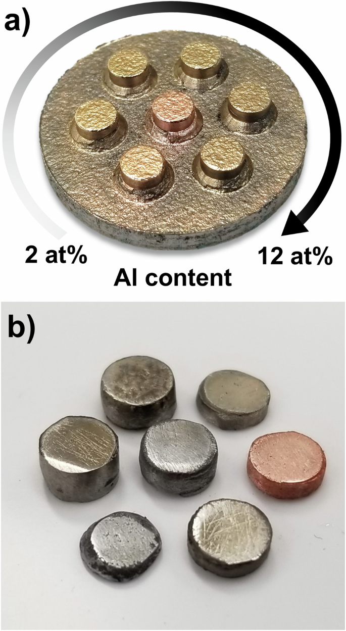
a a series of aluminum bronzes, featuring pure Cu in the center with increasing Al additions in the clockwise direction from 2 at% to 12 at%. b examples of individual elemental samples being produced simultaneously utilizing B4C as the pressure-transfer media.
Though largely successful at providing a proof-of-concept for the parallelized EFAS methodology, use of the machined monolithic tooling led to substantial drawbacks after the synthesis process during sample removal. At the temperatures and pressures necessary to densify materials during EFAS, the materials typically plastically deform to fill the shape of the tooling. However, in doing so, the sample arrays become press-fit into the graphite punch, making extraction of samples from the tooling, without damaging either, a difficult task. Moreover, due to the non-zero porosity of the graphite tooling, when a portion of the powder charge liquifies during consolidation (e.g., melting of Al in the formation of the aluminum-bronze array), the liquid metal can infiltrate the pores of the graphite tooling and solidify on cooling, further mechanically locking the samples or sample array into the tooling. While such phenomena are not unique to the parallelized EFAS process, the machined monolithic tooling suffers greater disadvantages as a result of these effects, as compared to traditional EFAS tooling geometries where samples are formed between the faces of two flat punches which can easily be sheared off to extract the sample. One phenomenon that causes perhaps outsized issues with parallelized EFAS tooling geometries arises from a mismatch in the coefficient of thermal expansion (CTE) of the tooling and the substrate material when producing arrayed samples. While at the elevated target temperature the substrate material is free to plastically deform and accommodate any stresses induced by a CTE mismatch. However, upon cooling, the now densified and increasingly rigid substrate material will contract, causing the protruding samples to be pulled closer to one another; since the CTE of the graphite tooling is far less than the CTE of most transition metals used for substrate materials20, the protruding samples impinge on the graphite tooling as they contract, further binding the sample arrays to the tooling. This effect becomes more prevalent with higher processing temperatures, where there is a greater change in dimension due to CTE relative to the room-temperature geometry, which can lead to the graphite divisions separating the recesses in the machined monolithic punch to be crushed during the cooling process, with little-to-no pressure applied externally. In sum, the machined monolithic tooling experienced a substantially higher attrition rate than traditional EFAS tooling, motivating the search for different tooling geometries.
Plunger-based design: variable geometries
In the pursuit of a tooling design better equipped for sample removal, a plunger-based design was examined. Instead of using recesses machined into the face of a punch, the plunger-based design involves drilling through-holes between both flat faces of the punch which can then be filled with graphite rods that are shorter than the full height of the punch, illustrated in Fig. 1b. The result is a geometry that is almost identical to the machined monolithic punch, except that the back of the plungers can be pressed to push the samples or sample array out of the tooling rather than requiring the user to pry the samples or sample array out from the top. The plunger-based design is also better equipped for producing different sample geometries and changing between sample geometries and orientations with less machining needed. Rather than having to machine recesses in a new punch to produce samples of different heights, the graphite plungers can instead be cut to different heights and shuffled around to produce any combination of sample height orientations versus the machined monolithic design which would have required a new punch for each orientation.
Capitalizing on the ease with which the plunger-based design can be used to produce samples of different geometries, and experiment was performed to determine the maximum practical aspect ratio of samples that can be produced using parallelized EFAS. To achieve this, a sample array of Cu pillars was produced using a plunger-based set of tooling, whereby a graphite punch featuring seven through-holes was filled with friction-fit graphite plungers of varying heights to effectively create an array of cavities of different depths. Each cavity was then filled with Cu powder before the entire punch face was covered with a Cu foil and loaded into a die where 15 grams of Ni powder was loaded above the filled punch, to serve as the pressure-transfer media, and subsequently consolidated to form the base plate of the sample array. The sample array was consolidated via EFAS with a pressure of 30 MPa, a target temperature of 1000 °C, and a dwell time of 5 min, after which it was readily extracted from the tooling by pressing on the plungers to push the sample array out of the custom punch. The resulting sample array is shown in Fig. 3, where the progression in sample height is readily visible. Also visible, is a narrow ring around the base of several of the Cu pillars, with what appears to be increasing prominence as a function of pillar height, initially thought to be related to the interface between the Cu and the Ni pressure-transfer media.
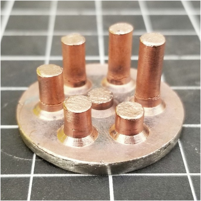
Varying pillar heights are produced by machining the height of the corresponding plungers in the plunger-based parallelized EFAS tooling.
Since the Cu pillars are attached to the Ni substrate, and the Ni extends to a yet unknown height in the pillar, traditional Archimedes’ density measurements would not be particularly insightful. Instead, each Cu pillar was sectioned longitudinally and imaged using optical microscopy, with the exception of the tallest Cu pillar which separated from the sample array at the ring feature visible in Fig. 3, during sample preparation. The stitched optical microscopy images of each Cu pillar are compiled and shown in Fig. 4. Here, the shortest Cu pillar is seen to be fully dense, with Ni powder extending past the chamfered edge and into the cylindrical portion of the pillar. The second shortest pillar is seen to be nearly fully dense as well, however regions of small pores are visible. From the third shortest pillar and onward, porosity becomes much more prevalent while the Ni does not appear to penetrate substantially farther up the Cu pillar and instead gives way to a more porous region near the Cu/Ni interface. Interestingly, the narrow ring feature around the base of the taller samples does not appear to occur at the Cu/Ni interface itself, but rather in the porous Ni region just below it. As such, it is posited that rather than a phenomenon related to the interface of the dissimilar materials, the ring may be an artifact of sample extraction from the tooling. Specifically, if pressure was not applied to the plungers equally during extraction (consider only pressure being applied to the center plunger in the array), the substrate would in effect be pulling against the frictional forces holding pillars in the tooling; this would explain the increased prominence of the ring feature as a function of pillar height, and the taller pillars would have greater frictional forces and greater porosity in the Ni region below the interface which would be more susceptible to necking.
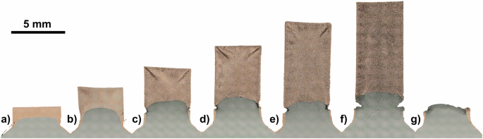
Target pillar heights including the chamfered bases are (a) 3 mm, b 5 mm, c 7 mm, d 9 mm, e 11 mm, f 13 mm, and (g) 15 mm.
At the intermediate aspect ratios, dark porous regions can be seen emanating from the corners at the tops of the pillars, which is not typical of EFAS-made cylindrical samples. In traditional EFAS, the die is only mechanically supported in free space by the frictional forces of the opposing punches, meaning as pressure is applied to one punch (e.g., the top punch) the die is free to slide until the pressure transmitted to the other punch (e.g. the bottom punch) balances it. All things being equal, with equal pressures on each punch face, the pellets produced would be expected to have symmetric density profiles along the axial direction. However, for powder compaction with a supported die, die wall friction can lead to a decrease in the transmitted pressure between the actuated punch and the reactionary punch, leading to an asymmetric axial density profile21. In the case of the plunger-based design, the custom punch which houses the plungers is mechanically supported by the ram in the EFAS system, enabling a drop in the pressure transmitted to the face of each plunger relative to the pressure applied by the pressure-transfer media. Indeed, the decreased density at the corners of the Cu pillars agrees with density profiles from green-body powder compaction experiments and modeling efforts in literature22, however the exact density profile will also depend on the temperature distributions and local current densities during the parallelized EFAS process.
To more quantitatively assess the density of the Cu pillars as a function of pillar height, the stitched optical microscopy images from Fig. 4 were thresholded into binary images, using the software ImageJ, where the porosity could be quantified. Areal density, which is calculated as the ratio of solid area to the total area evaluated, is used to determine density of the pillars. The results from the image analysis are given in Table 2. From the results, it is evident that for the straight-walled, 5-mm-diameter, cylindrical sample geometry, substantial porosity is incurred at aspect ratios much above 1:1. Additionally, the areal density of the 13-mm-tall Cu pillar was found to be 68.75%, which is only marginally greater than values typical of green-body powder compacts, suggesting that for aspect ratios approaching 3:1, the processing conditions begin to approach that of pressure-less sintering.
The plunger-based tooling design offers substantial improvements over the monolithic design with regards to sample extraction as well as customizability, by virtue of being able to reconfigure the tooling by rearranging or exchanging the plungers. Greater sample aspect ratios may also be able to be achieved by increasing the starting density of sample powders loaded into the tooling, for example by using a mixture of powders with a bimodal or even trimodal size distribution to increase packing density23. Yet, the addition of the plungers leads to greater vulnerabilities with certain materials and process conditions. For example, during liquid phase sintering, the slip-fit interfaces between the plungers and the surrounding punch can serve as highways for capillary action which can wick the liquid metal deeper into the tooling and subsequently freeze during cooling, preventing the plungers from being removed non-destructively. Since additional coatings or foil liners are unlikely to sufficiently impede the mobility of liquid metal, the plunger-based tooling design appears best reserved for sintering operations which occur in an entirely solid-state regime.
Insert-based design: high-entropy alloy compositional array
The final optimized custom tooling design took a different approach from previous iterations. Rather than add additional features to relatively large custom punches in an attempt to thwart tool failure mechanisms, a smaller, consumable, tooling insert was designed. The tooling insert developed (illustrated in Fig. 1c) consists of a thin disk of graphite with series of through-holes drilled for the sample recesses. The holes themselves are conical frustums with a constant taper of 15° which provides multiple benefits: (1) by broadening the opening of the holes on the substrate side and adding a constant taper, effects of stress shielding from die-wall friction can be reduced leading to greater, more uniform densities, and (2) by introducing tapered recesses, during cooling, net contraction of the substrate material relative to the tooling provides an uplift force as the protruding samples are pressed against the tapered tooling walls, which acts to separate the sample array from the tooling. Moreover, by using a thin graphite insert, which can be easily attached to a standard flat punch using graphite foil and a cyanoacrylate-based adhesive, the volume of graphite tooling is susceptible to damage during parallelized EFAS is reduced significantly—so much so that the inserts can be easily produced and treated as lower cost consumables. Other sample and data management features such as fiduciary marks, which are mirrored onto the substrate during sintering, and flats around the periphery of the insert, to aid in sample extraction, were added. The substrate outer diameter was 31.75 mm (1.25 in) to fit the form factor of the sample holders for both the scanning electron microscope (SEM) and autopolisher used for characterization and sample preparation, respectively.
To assess the viability of using parallelized EFAS for complex alloy discovery, a compositional series of equimolar alloys was made from mixtures of elemental powders consisting of the following compositions: Ni, CoNi, CoCrNi, CoCrFeNi, CoCrFeMnNi, CoCrCuFeMnNi, AlCoCrCuFeMnNi. Mixtures of the elemental powders were loaded into separate sample recesses in the insert-based tooling; the filled recesses were then covered by a single piece of low-carbon steel foil which was then topped by 20 g of Ni powder to serve as both the pressure transfer media and subsequent substrate material. To consolidate the materials, a pressure of 50 MPa was applied to the tool stack while the temperature was ramped and during the dwell. Previous EFAS experiments using elemental powder mixtures of the Cantor alloy (equimolar CoCrFeMnNi) composition encountered unexpected melting substantially below the reported melting point of the alloy. The root cause of this is thought to be the formation of a low-melting-point mixture of the Ni and Mn powders, which in near equimolar ratio begin to melt as low as 1020 °C24. To mitigate this hazard, the temperature during the parallelized EFAS ramp was brought to 900 °C at 50 °C/min then to 1000 °C at 25 °C/min followed by a 15-minute dwell, to allow for interdiffusion of Mn and Ni with other elemental powders, before finally climbing to 1150 °C at 10 °C/min. The system was held at 1150 °C for 1 h before the power was turned off and the pressure was reduced to 5 MPa to minimize the applied pressure during cooling, while still providing adequate thermal contact for heat removal. The compositional array, following extraction from the graphite insert and cleaning with a wire brush, is pictured in Fig. 5. Here, the extent of the Ni penetration into the sample recesses can be observed as a change in color and surface roughness along the sides of the samples, located between ~25–50% the height of the sample as measured from top of the substrate.
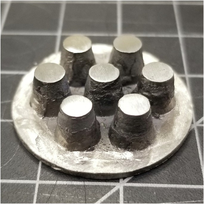
Ingress of the Ni pressure-transfer media into each of the recessed cavities is observable as a step change in color and texture along the side of the synthesized samples.
The seven samples on the compositional array were mechanically polished simultaneously to a final polishing step of 0.05-μm colloidal silica with all of the samples remaining well adhered to the substrate. Minor interaction with the graphite tooling was observed resulting in a carburized rind on the outer surfaces of each sample with a thickness on the order of hundreds of microns, however this was readily removed during mechanical polishing. Following sample preparation, SEM and EDS were performed, the results of which are summarized in Fig. 6. Here, each of the samples appears to be effectively fully dense, with grain sizes multiples times larger than the starting average particle sizes. The average grain size begins at >100 microns, in the case of Ni, and monotonically decreases to ~10 microns with increasing compositional complexity, with the exception of the senary HEA, CoCrCuFeMnNi, whose grains appear larger than its less chemically complex neighbors. In most of the Cr-containing alloys, Cr-rich inclusions are present where Mn also tends to co-locate once introduced. From the EDS mapping, some mesoscale compositional variation is visible, in what would otherwise be expected to be chemically homogeneous regions. Starting with CoNi, for example, there appear to be “hot spots” of Ni and Co larger than the individual grains of the material. Since these hot spots are larger than the starting powder size and appear to cross over multiple grains, it is thought that these are the result of insufficient mixing during the powder preparation step and could likely be eliminated with longer mechanical mixing and/or longer EFAS dwell times. Such hot spots are also present for subsequent alloying elements and appear to be exacerbated in compositions with large fractions of Cr and Fe, while additions of Mn, Cu, and Al appear to smooth out compositional variation.
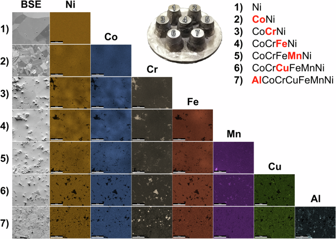
1 Ni, 2 CoNi, 3 CoCrNi, 4 CoCrFeNi, 5 CoCrFeMnNi, 6 CoCrCuFeMnNi, and 7 AlCoCrCuFeMnNi. The scale bar in each image is 50 μm.
To illustrate the stark difference in microstructural complexity between the higher order HEAs, Fig. 7 shows secondary electron SEM images of CoCrCuFeMnNi and AlCoCrCuFeMnNi taken at a magnification of 5000x. For the six-component HEA, CoCrCuFeMnNi, the microstructure largely consists of single phase with minor secondary phases decorating the grain boundaries. In contrast, by adding ~14 at% Al to this alloy to form the seven-component HEA, AlCoCrCuFeMnNi, the microstructure separates out into at least four distinct phases, not including any oxides or inclusions from the starting powder mixtures. Within the microstructure of AlCoCrCuFeMnNi, several grains are filled with sub-micron intragranular precipitates exhibiting a fourfold symmetry and periodic spacing. This regular spacing and morphology is indicative of either a coherent or semi-coherent precipitate/matrix interface, which is often observed in microstructures featuring ordered precipitates in a disordered matrix which shares a similar crystal structure, such as γ/γ’ in Ni-based superalloys25 and BCC/B2 in refractory HEAs26,27.
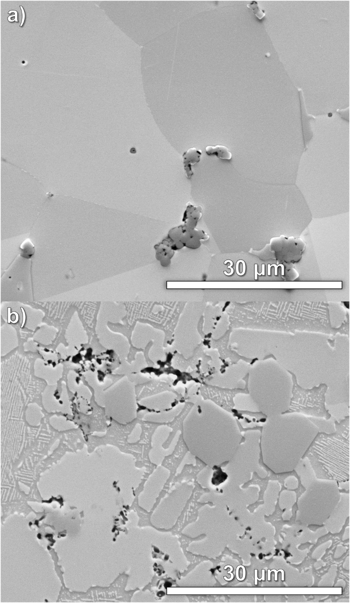
The microstructure of (a) the six-component HEA, CoCrCuFeMnNi, consists of a predominant single phase while the microstructure of (b) the seven-component HEA, AlCoCrCuFeMnNi, exhibits a substantially more complex microstructure.
Phase identification of the samples in the compositional array was carried out using XRD, the results of which are presented in Fig. 8. Here, all samples exhibit a prominent face-centered cubic (FCC) phase, identifiable by the pairs of peaks at 2θ values of approximately 43° and 50° and near 90° and 96° as well as the prominent peak near 75°. Pure Ni and the CoNi binary appear to be single-phase FCC structure, while the addition of Cr to form CoCrNi gives rise to series of minor, low-angle peaks which are thought to be associated with chromium oxide inclusions rather than any unreacted Cr powder since none of the major BCC reflections associated with elemental Cr were observed. With the addition of Fe, a prominent peak appears on shoulder of the first FCC reflection along with a series of new minor peaks most often associated with a tetragonal sigma phase (σ)28. Further additions of Mn and even Cu appear to have little effect on the phase makeup of the alloys, with CoCrFeNi, CoCrFeMnNi, and CoCrCuFeMnNi all exhibiting a predominately FCC microstructure along with the presence of a σ phase. From the EDS chemical mapping in Fig. 6, the Fe and Cu additions tend to segregate to the FCC phase while the Mn tends to co-locate with Cr in the σ phase. With the addition of Al to form the septenary HEA, a prominent BCC phase arises as indicated by the peaks in the XRD spectrum at approximately 44°, 64°, 81°, and 97°. While an ordered phase is also anticipated based on the SEM results from Fig. 7, it is unclear from the XRD spectrum alone what crystal structure the ordered phase might be. The main challenge is that the primary peaks for ordered phases (e.g., L12, L10, B2) are coincident with the peaks of their disordered counterparts, while the “forbidden” peaks necessary for phase identification are typically much more subtle, based on the difference in X-ray scattering intensity between the two sublattices. The intensity of the forbidden peaks also has the potential to be further muted in HEAs compared to binary systems depending on the composition of atoms on each sublattice. For example, if a sublattice composed solely of A and B atoms had the X-ray scattering intensity as a sublattice composed solely of C and D atoms, it would be impossible to distinguish this decidedly ordered structure from a completely disordered mixture of A, B, C, and D atoms on the same lattice through XRD alone.
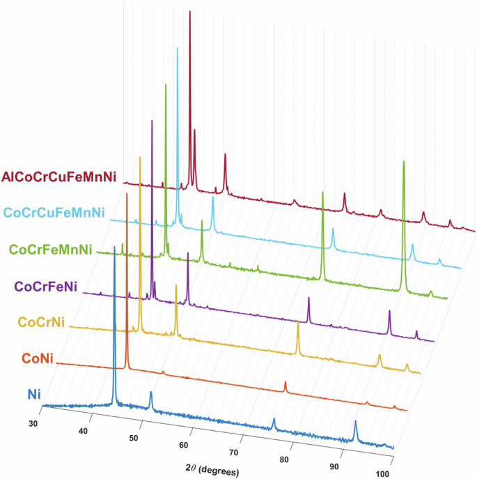
All alloys exhibit a significant FCC phase fraction, with simpler compositions remaining almost entirely single-phase FCC while more complex compositions begin to exhibit multi-phase characteristics including the presence of one or more BCC phases, including the possibility of ordered phases.
To further elucidate the phases observed in the SEM/EDS and XRD analyzes, CALPHAD simulations were performed to assess the thermodynamically stable phases for each alloy composition from 0 °C to 2000 °C, presented in Fig. 9. Pure Ni was omitted as it is sufficiently described elsewhere in literature. Most of the alloy compositions feature a large single-phase FCC region below the melting point, with the exceptions of CoCrCuFeMnNi and AlCoCrCuFeMnNi that are not thermodynamically expected to exhibit a single-phase solid solution at any temperature. With the exception of CoNi, all of the alloys are expected to form several secondary phases at lower temperatures, and both the number and phase fraction of secondary phases seem to increase with each additional element. Despite any counteraction from the proposed “high-entropy effect”29, many of the secondary phases expected to form are not solid solutions, and are instead ordered phases with preferred lattice site occupancies often dominated by a single element (e.g., Cr in σ).
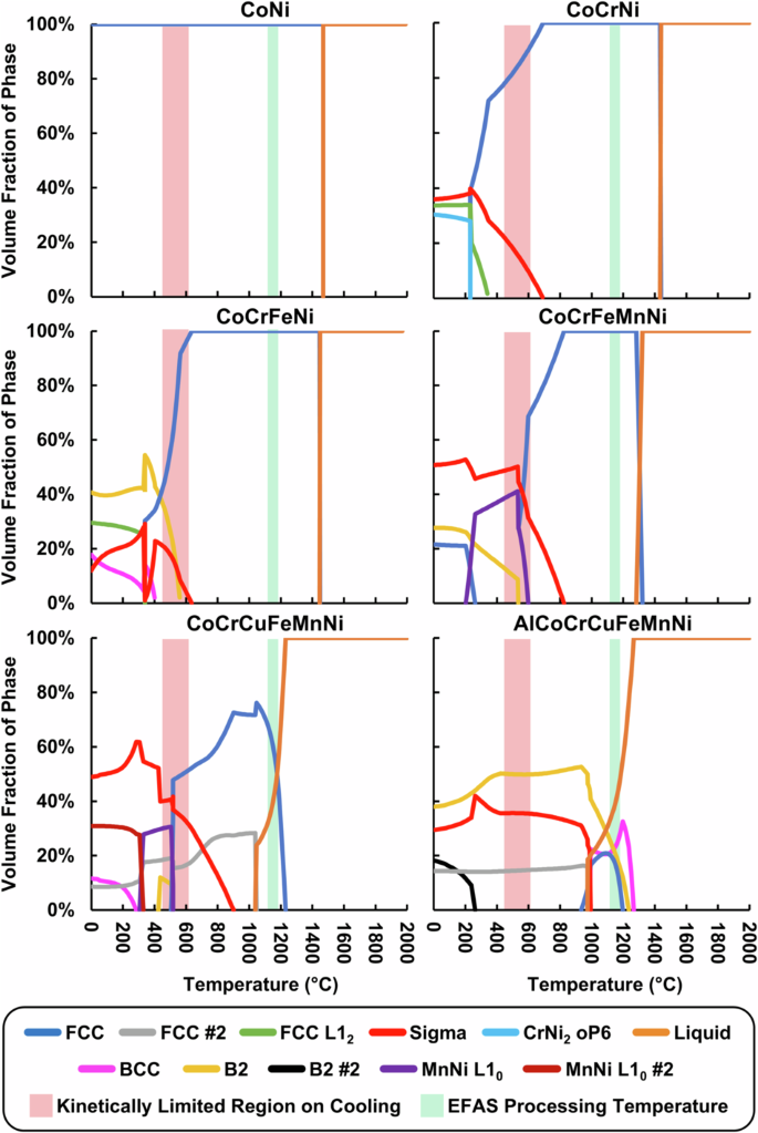
The maximum EFAS processing temperature during synthesis and the approximate temperature range at which precipitation kinetics are sufficiently slow to impede new phase formation are indicated for better rationalization of in situ alloying behavior versus resultant microstructures observed ex situ.
Scalability Assessment
While bench-scale production of samples is a necessary step in process development, broader adoption of a technique requires scalability. To assess the feasibility of scaling the parallelized EFAS technique to both larger samples and greater numbers, the insert-based tooling design was adapted to produce a 75-mm-diameter plate featuring 19 samples, each with a diameter of 12 mm at the base and 8 mm tall, pictured in Fig. 10. Prior to filling with powder, the custom graphite insert was coated using a boron nitride (BN) spray to both improve part extraction and to shunt electric current through the powder-filled recesses rather than the insert itself, as higher current densities would be expected to enhance diffusion during the sintering process30. Mixtures of elemental powders were prepared and loaded to produce the equimolar CoCrFeMnNi HEA along with duplicates featuring a series of increasing minor alloying additions, consisting of 1 at% to 6 at% additions of Al, Cu, and Ti. In light of the deleterious σ phase forming in the small-scale compositional array, efforts were made to accelerate the cooling rate of the sample array after synthesis by omitting the carbon felt which is typically wrapped around the die during sintering. Once assembled, the materials were processed using a larger EFAS system (Thermal Technology DCS-25), capable of accommodating the larger toolset, while using the same peak temperature, pressure, and dwell time as the small-scale compositional array (1150 °C, 50 MPa, 1 h, respectively).
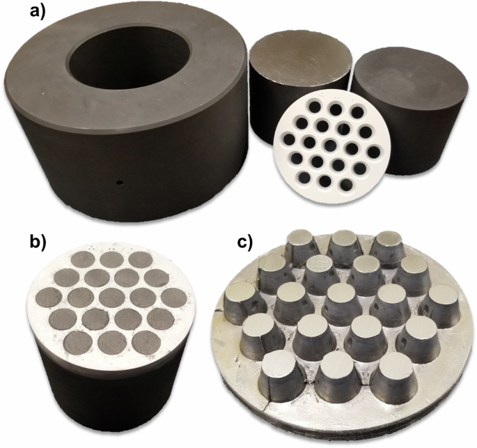
a 75-mm-diameter graphite tooling featuring BN-coated custom insert. b tooling filled with powder charges prior to sintering. c Resultant compositional array after synthesis.
Following synthesis via parallelized EFAS, the 19-sample array was mechanically polished and characterized in the same manner as the small-scale HEA array. A carburized rind was observed on each of the samples, characteristically similar to that of samples from the small-scale HEA array, however the overall volume fraction of the rind was smaller in the case of the 19-sample array owing to the larger sample sizes. SEM images of each of the 19 samples are shown in Fig. 11 along with EDS mapping of the base equimolar CoCrFeMnNi alloy. From the EDS mapping of CoCrFeMnNi, the material appears to be largely homogeneous at the mesoscale, however smoothly varying hot spots akin to those found in the small-scale HEA array remain visible. While Cr-rich regions, and even some Mn-rich regions, do still exist, their presence directly correlates to the oxygen-rich features in the EDS mapping, suggesting the presence of oxides entrained from the starting powder rather than a secondary phase forming from the base metallic alloy. In examining the CoCrFeMnNi alloys featuring minor alloying additions, it appears additions of Al, Cu, and Ti up to 6 at% do not appreciably destabilize the predominately single-phase FCC microstructure exhibited by the base alloy under these processing conditions. Despite this, similar trends in grain size are observed for Cu and Al additions as were observed in the small-scale HEA study: with increasing Al content, the grain structure becomes more refined while with increasing Cu content, the grain structure coarsens. While not included in the small-scale HEA study, the addition of Ti appears to have a similar effect to Cu, in that increasing additions of Ti appear to coarsen the grain structure.
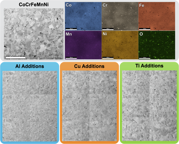
Samples are observed to be largely chemically homogeneous with a presence of oxide particles likely entrained from the starting powders.
Discussion
From the CALPHAD simulations of the small-scale compositional array, the four simplest alloys are all expected to form a single disordered FCC phase at the EFAS sintering temperature of 1150 °C, while the six- and seven-component HEAs both have a considerable liquid phase fraction at these temperatures indicating that liquid phase sintering was likely occurring for these materials during the parallelized EFAS process. This liquid phase sintering is likely responsible for the marked grain growth observed in the CoCrCuFeMnNi sample as compared to its less chemically complex predecessors. While AlCoCrCuFeMnNi also likely underwent liquid phase sintering, at 1150 °C, AlCoCrCuFeMnNi has three solid phases (FCC, BCC, B2) competing with the liquid phase, which likely slowed the grain coarsening process relative to CoCrCuFeMnNi which only is expected to have a single FCC phase coexisting with the liquid phase at that temperature.
Since only the pure Ni and CoNi samples were characterized to have a single-phase FCC microstructure, it is likely that the natural cooling rate of the EFAS tooling was not sufficient to avoid the formation of secondary phases at lower temperatures. Given the observation of the σ phase in the otherwise FCC CoCrNi, CoCrFeNi, and CoCrFeMnNi alloys, in conjunction with the lack of many of the phases predicted by CALPHAD at low temperatures, it appears that the precipitation kinetics slowed appreciably below ~600 °C preventing additional phases from forming during cooling. Using 600 °C as a reference temperature, highlighted for reference in Fig. 9, the characterization results for the higher-order HEAs can be compared against CALPHAD predictions. In the case of CoCrCuFeMnNi, two FCC phases and a σ phase would be expected from CALPHAD while SEM/EDS suggests two primary phases are present, which from XRD were determined to be FCC and σ. While only one FCC was detected through initial characterization efforts, it could be possible that a second FCC exists. For example, if the two FCC phases are forming as part of a spinodal decomposition from a single original phase, the length scale of the chemical variation could be below the resolution of the SEM imaging and EDS mapping, while the lattice parameters of the two nascent phases may be too close to be distinguished with lab-scale XRD. Some enrichment of Cu is visible at the grain boundaries; however, it is not clear if this is microchemical segregation originating from the liquid phase sintering occurring or if this is indeed a separated phase. As such, further higher resolution characterization techniques would need to be employed, such as transmission electron microscopy (TEM), atom probe tomography (APT), or synchrotron XRD to definitively rule out the possibility of a second FCC phase in the CoCrCuFeMnNi sample. In the case of AlCoCrCuFeMnNi, one FCC, one σ phase, and one ordered B2, would be expected at 600 °C based on CALPHAD. This compares well with the XRD results, which also indicate the presence of an FCC phase, a σ phase, and either a BCC or B2 phase. However, EDS mapping and SEM imaging in Figs. 6 and 7 suggest the presence of at least four different phases, which could be the result of phases stable at the higher EFAS sintering temperature (1150 °C) being partially retained after cooling. Specifically, it is posited that the fine precipitates observed in Fig. 7b are an ordered B2 phase which forms a coherent/semi-coherent interface with a disordered BCC phase retained from the high-temperature dwell. The presence of an additional disordered BCC phase with a similar lattice parameter to the observed B2 precipitates is still supported by the XRD spectrum, since the peaks of the two phases would largely overlap, and appears plausible considering the CALPHAD predictions and thermal history of the sample. However, much like CoCrCuFeMnNi, definitive determination of the presence of both BCC and B2 phases in AlCoCrCuFeMnNi would likely require higher resolution characterization techniques. Finally, notwithstanding experimental uncertainties, it should be noted that the predictive capability of CALPHAD simulation is incumbent on well populated thermodynamic databases while historically the thermodynamics of multi-component, equimolar alloys has been substantially under-populated with experimental data as compared to alloy systems already used in industry (e.g., steels, Al alloys, Ni alloys, etc.). As such, some of the greatest uncertainties and deviations would be expected from CALPHAD predictions of complex, multicomponent systems which can be exacerbated when considering dynamic systems (e.g., the slow cooling of the compositional arrays from elevated temperature) where knowledge of diffusion kinetics is necessary to make accurate predictions of the phases present after a given thermal treatment. Consequently, this touches on one of the potential use cases of parallelized EFAS: populating thermodynamic and kinetic databases for HEAs, since arrays of HEAs can be synthesized, heat treated, and characterized in a high-throughput fashion.
Through both the large-scale and small-scale HEA compositional arrays, the viability of the parallelized EFAS technique for alloy screening was largely proven, as multiple alloys with melting points spanning ~500 °C were synthesized simultaneously and found to be nearly fully dense with little evidence of unreacted elemental powders. However, there is still substantial room for improvement on the feedstock development, regarding both quality and efficiency. Specifically, as evidenced by the EDS mapping in both Figs. 6 and 11, several hot spots locally enriched in one element appear in the alloys that were not assisted by liquid phase sintering at elevated temperatures, indicating further mixing of the elemental powder blends is needed prior to die loading. This practically might be accomplished by increasing the Turbula mixing time and/or by including ball bearings or other media in the powder container during mixing which can assist in breaking up clumps and aggregates of powder without introducing contamination. Rather than mixing elemental powders, high-energy ball milling or related techniques could be used to mechanically alloy the powders prior to consolidation which would reduce the sintering temperatures and durations required to produce homogeneous samples, however this would dramatically increase the powder preparation time from hours to days depending on the number of alloy compositions needed. As with any powder-based synthesis technique, impurities in the starting powder can be detrimental. In the case of metal powders, oxides present on reactive metal powders (e.g., Cr, Mn, Ti, and Al) are typically incorporated into the final sample, and the oxide fraction of the starting powder typically increases as powder size decreases owing to the increased surface area. As such, the drive to opt for finer powders to improve chemical homogeneity is countered by the need to minimize oxide impurities, unless a chemical reduction (e.g., hydrogen reduction) step is performed on the powder prior to sintering.
Notwithstanding challenges associated with feedstock materials, the parallelized EFAS process provides immense timesaving over traditional EFAS when producing multiple samples. In comparison to traditional EFAS sample making, the powder processing and die loading times are almost identical, however, since all of the samples are consolidated simultaneously during parallelized EFAS, the synthesis time per sample goes as ~1/n, where n is the number of samples. In the small-scale HEA case study, for example, with seven samples being synthesized in parallel, the EFAS processing time required was ~14% of the time needed traditionally, while also saving energy due to the reduced radiative heat loss per unit volume when using larger-diameter tooling (to accommodate the array of samples) versus multiple EFAS runs with smaller-diameter tooling. Similarly, the large-scale array featuring 19 samples only required ~6% of the processing time on a per-sample basis, deviating from the 1/n scaling only marginally due to the slower cooling rate of the larger tooling employed. In theory, there is no hard limit on the number of samples that can be produced simultaneously that would result in such timesaving, however there are practical limits on how small the samples could be made or how large the physical EFAS apparatus could be. For example, as samples get smaller, the metal foil which separates the sample powder from the pressure transfer media would require greater pressures to be able to deform at the tighter radius of curvature needed to transfer pressure to the sample powder; at a sufficiently small sample size, the pressure transferred to the individual samples would become negligible without using an applied pressure greater than the tooling could withstand. Moreover, if high temperatures and long dwell times are used, interaction of sintered articles and the tooling (e.g., carburization) becomes a greater issue as sample size decreases; for a given set of temperatures, times, and sample chemistries there will be a given thickness of an interaction layer with the tooling and as the sample size decreases this interaction layer will represent a larger fraction of the overall sample volume, effectively producing less usable material. On the other hand, if the sample size is kept constant but the number of samples is increased, then larger tooling and larger systems would be required. While both larger systems and larger sets of tooling are certainly available, there can be additional costs encountered depending on the scale of the system. For example, as the tooling size increases, the temperature ramp rates and cooling rates must be slowed down to minimize stresses induced by thermal gradients in the tooling which can jeopardize the survivability of the tooling. Such thermal gradients can also begin to affect the microstructural uniformity of parts produced in parallel. At smaller scales and using a thermally conductive pressure-transfer media (Ni), negligible microstructural variation was observed that could be attributed to thermal gradients, as evidenced by the grain sizes of samples in the 19-sample array varying monotonically with minor changes in composition despite each compositional set utilizing at least three unique radial positions within the tooling. As tooling size increases and especially if electrically and thermally insulating pressure-transfer media is used, minimization of thermal gradients will likely require bespoke tooling to direct the electric current in such a way that more uniform heating can be achieved. At much larger scales, tooling -especially graphite- can be more difficult and costly to source such that an insert-based technique which features consumable tooling becomes practically infeasible. Considering these extreme limits and compared to traditional single-sample EFAS, however, the parallelized EFAS process is expected to remain substantially more time and cost effective over a broad range of length scales beyond the sample geometries chosen for the HEA case study presented here.


Responses