Operando evaluation of passivation phenomenon during ECM/Laser-ECM: direct and on-machine evidence of passivation evolution

Introduction
Electrochemical micromanufacturing technologies encompass electrochemical micromachining1,2, electrochemical additive micromanufacturing3 and electrochemical postprocessing technologies4, and form a major class of athermal manufacturing technologies especially for high-end components required amongst others in semiconductor5, mould manufacturing6, processing of advanced materials7 and aerospace2. Electrochemical micromachining (ECM) is a non-contact machining process where the material removal is achieved by virtue of anodic dissolution of electrically conductive workpiece where the rate of dissolution is determined by Faraday’s laws. During ECM, several multi-physical phenomena occur in the interelectrode gap, which have been a focus of fundamental studies to improve understanding towards better process monitoring and optimisation. Passivation is one such phenomenon where a 10–20 nm non-conductive surface oxide layer dynamically evolves during ECM and subsequently hinders material dissolution and hence, plays a critical role in determining the EC-dissolution kinetics and surface integrity alongside selective dissolution, pitting and particle breakout mechanisms8. In addition, with the development of novel materials like bulk metallic glasses7, high entropy alloys9 and cermets10 to improve process efficiency and for applications in harsh mechanical, thermal and corrosive environments, the issue of passivation is further magnified. These advanced materials consist of multiple phases, each with a varying degree of passivation tendency which results in uneven material dissolution with ECM. Therefore, it is necessary to develop an on-machine technique for analysing passivation to capture comprehensive production-oriented information with process history of passivation to support fundamental mechanistic investigations. In addition, on-machine passivation information at different processing conditions can facilitate manufacturers to devise process optimisation strategies in order to improve processing performance and ensure good surface integrity.
Generally, an offline passivation analysis approach is employed as depicted in Fig. 1a, d–g as it is difficult to implement sensors (e.g. gas sensor) and chromatography techniques in the small interelectrode gap (<200 µm). The sample is observed through metallography techniques like scanning electron microscopy (SEM), energy dispersive X-ray spectroscopy (EDS), computed tomography, etc. to gather microstructure information (Fig. 1d) and element mapping of the machined surface (Fig. 1e) to correlate with the passivation behaviour. The collected data is then manually analysed for visualisation (Fig. 1g). However, it only provides oxide formation data after machining in a localised observation window. It lacks comprehensive information about component level production as the collected data cannot be extrapolated to the part level due to the limited number of observations, sporadic distribution of passivation on workpiece surface, repeatability and limitation on observation area. Furthermore, the metallography analysis is usually supplemented with voltammograms (Fig. 1f) obtained through potentiometric techniques like linear sweep voltammetry (LSV), open circuit potential (OCP), electrochemical impedance spectroscopy (EIS), etc11. However, the potentiometric techniques11,12 have limitations for analysing passivation since the high voltage and current density conditions (>15 V, >70 A/cm2) of ECM cannot be replicated. The passivation behaviour and transpassive dissolution can be different during ECM than the low voltage and current conditions of potentiometric measurements. In addition, in some cases as this study, especially for advanced materials with multiple phases, the ECM passivation and removal behaviours overshadow the first principles13 based potentiometric conclusions14.

The on-machine approach involves a machining the samples, b acquisition of in-process current signal, c postprocessing and statistical analysis of the current data, and g quantitative analysis of passivation. The offline approach involves a machining, d microstructure analysis of the material, e element mapping through metallography and f voltammograms through potentiometric techniques, and g qualitative analysis of passivation. h The proposed approach can be further developed and implemented into digital twins of ECM/LECM.
Hence, we propose an on-machine analysis framework as illustrated in Fig. 1a–c, g to capture the dynamic passivation phenomenon during part machining with process history. It is based on the in-process current signal which reflects the change in the overall interelectrode gap resistance and capacitance induced by passivation. It involves acquisition of the in-process current signal at high frequency (10 MHz) through a digital oscilloscope (Fig. 1b) and processing the current data by defining indicators based on expert theoretical and experimental ECM knowledge (Fig. 1c) to provide quantified estimation of passivation with process history (Fig. 1g). This framework provides quantified part machining information of operando passivation phenomenon which is useful for mechanistic process investigations and relevant for component level production.
In order to evaluate the proposed on-machine passivation analysis framework, Ti6Al4V was employed as a workpiece material due to its highly passivating nature in aqueous electrolytes15,16,17 and strategic applications in aerospace and biomedical sectors. In addition, samples prepared through rolling and selective laser melting (SLM) were used to investigate the proposed framework against different manufacturing processes induced microstructure18 and porosity19 of the same material. Ti alloys are key industry materials with applications in several sectors like, automotive, aerospace, biomedical, etc. due to lightweight, corrosion resistance, high strength, high hardness, biocompatibility and thermal stability at extreme temperatures. However, the high strength and low thermal conductivity create machining challenges for Ti alloys20, which are further magnified for microscale features. ECM can process Ti alloys athermally to preserve material properties15, but it requires material removal localisation strategies to reduce overcut through tool insulation21, tool design and electrolyte flow field optimisation22, pulsed ECM23, hydraulic jump in jet-ECM24 and bi-polar pulsed ECM to leverage H2 bubbles generation as an insulation layer25, among others. In addition, the highly passivating nature of the Ti alloys leads to inhomogeneous material dissolution in aqueous pH-neutral salt electrolytes16, which require high current densities (>300 A/cm2)26 and salt concentrations (20%)27 to overcome the passive layer resistive barrier. Alcohol based electrolytes which were previously used for mirror electropolishing28 have recently shown promising results for machining Ti alloys. Ethylene glycol-based electrolytes can homogenously process Ti alloys as the absence of water mitigates passive layer formation29. However, these electrolytes suffer from low current efficiency which limits their industrial scalability and the research is still on-going. Therefore, hybridisation of ECM with other process energies is being researched to machine advanced materials with good precision and surface integrity, while maintaining high productivity30. Here, we employed the recently developed hybrid laser-ECM (LECM) technology14,31 to weaken passivation in aqueous electrolyte and machine Ti6Al4V without thermal defects and chips formation (necessary for transparent gap) as opposed to other ECM processes hybridised with thermal (ECDM)32 and mechanical (ECM-grinding)33 energies, respectively. LECM is a hybrid machining approach34 which can simultaneously apply laser and EC process energies at the same machining zone, which improves ECM material processing windows and capabilities by increasing the local current density, weakening the passive layer and enhancing reaction kinetics35, making it promising for processing Ti6Al4V. In addition, aqueous sodium nitrate (NaNO3) electrolyte was used to create passivation favourable machining conditions to facilitate passivation analysis.
Here, we present a framework for on-machine passivation analysis based on high frequency in-process current signals to investigate the dynamically occurring passivation phenomenon and provide a holistic perspective of the passivation influence with its process history (effective machining time, passivation evolution) during part machining. We demonstrated that the proposed operando passivation analysis framework is sensitive to different processing conditions and microstructure of the same material (Ti6Al4V). The results show that it can holistically capture passivation behaviour as compared to the localised analysis using metallography approach, and provides quantitative information about passivation evolution during ECM and LECM. The conclusions inferred from the current pulse analysis were supported by high-speed camera observations, open circuit potential (OCP) measurements and cavity machining experiments to further validate the feasibility of the proposed framework. Therefore, this framework can serve as a tool for fundamental mechanistic studies on electrochemical manufacturing of advanced materials. However, further research is needed in the ECM field to develop in-process signal analysis techniques to analyse various process-material interactions at different time scales to enable development of digital twins of ECM and LECM2 towards adaptive process control (Fig. 1h).
Results
Framework for on-machine evaluation of passivation
We selected the in-process current pulses (at 10 MHz sampling rate) to analyse passivation as the change in current flow through the interelectrode gap indirectly reflects the material removal behaviour influenced by the dynamic passivation phenomenon as governed by Faraday’s law. The increase/decrease in surface passivation affects the overall interelectrode gap resistance which corresponds to the decrease/increase in material removal. This resistance change induced by passivation can be captured by the current signal for passivation analysis. Therefore, we developed a framework for high frequency current pulse analysis for on-machine passivation analysis and is provided in Fig. 2a, which considers both the pulse duration and current values to provide a comprehensive quantitative estimate of passivation influence and its process history during part machining. The in-process current pulses acquired through the digital oscilloscope were first observed at different time scales to define possible indicators for passivation during Ti6Al4V processing. The magnified view of the current pulse in Fig. 2a shows that the pulse shape changed according to the degree of passivation depending on the processing condition. The pulse turned OFF abruptly, resulting in pulse width reduction (tRON) and at certain instances it stayed OFF (tOFF’) even though the voltage was applied as per the designed pulse-ON condition (tON). Since Ti6Al4V is a highly passivating material, at processing conditions with limited passivation weakening (low voltage), after certain level of passivation layer growth the resistive barrier becomes too high for current flow, resulting in the tRON and tOFF’ states. Therefore, tOFF’ represents the duration of machining time spent without effective machining. In addition, during each tON pulse duration, the current continuously decreased due to passive layer formation. Based on these observations the following pulse duration and current indicators were defined for quantitatively analysing passivation:
-
i.
tON’: To quantify the duration the current pulse actually stayed ON (actual machining time).
-
ii.
tRON: To quantify the duration the current turned OFF abruptly (pulse width reduction, abrupt stop in machining).
-
iii.
tOFF’: To quantify the duration the current pulse stayed OFF during tON condition (duration where no effective machining occurs).
-
iv.
Pulse drop: To quantify the drop in current values during each tON duration (dynamic passivation growth during each pulse).
-
v.
Avg. Current: To quantify overall current data (overall passivation influence).
-
vi.
Max. Current Value: To quantify the highest current flow condition (highest passivation weakening condition).

a In the proposed framework, the raw in-process current pulses were analysed to define current and pulse duration indicators. Thresholding approach was used to calculate the current indicators (pulse drop, avg. current, max. current value). Data count approach was used to calculate the pulse duration indicators (tON’, tRON, tOFF’). The indicators were used for pulse classification and subsequent statistical analysis. b The sample pulses show that passivation weakened with increasing voltage and LECM, as demonstrated by decreasing tRON and tOFF’ states. The current values of SLMed samples were lower than rolled samples, indicating a more corrosion-resistant microstructure.
The sample pulses for different processing conditions are provided in Fig. 2b. Upon visual inspection, the increasing current values and decreasing tOFF’ states with LECM processing for both materials already indicate increase in transpassive dissolution and passivation weakening. Also, the current values of the SLMed samples were almost half of the values for the rolled samples, which suggest that the material was more resistant to EC-dissolution. Therefore, we utilised the on-machine current pulse analysis framework to quantitatively evaluate passivation evolution and transpassive dissolution kinetics during different processing conditions. In addition, the millisecond36 fluctuating current pulse trend with ECM at 40 V (Fig. 2b) for both the materials possibly represents unstable processing conditions as a consequence of excessive intermittent joule heating, since the electrolyte flow rate was insufficient for flushing to maintain stable interelectrode gap conditions. This suggests that depending on the time scale of current pulse analysis, different frameworks and indicators can be developed for analysing removal behaviour and monitoring gap conditions37 in real-time, which will be explored in the future.
On-machine evaluation of passivation
In order to test the proposed current pulse analysis framework for on-machine passivation analysis, the machined samples (machining time of 10 s) were also characterised through the traditional metallography approach for comparison. The SEM micrographs in Fig. 3 show the difference in surface morphology as a consequence of passivation and removal behaviour at the different processing conditions and the influence of sample manufacturing process.

The surface morphologies of a–e rolled samples show improved passivation weakening with increase in voltage and LECM, but at 40 V it is aggravated. The surface morphologies of g–k SLMed samples show uneven removal due to preferential pore site dissolution which was reduced with increase in voltage and LECM, but at 40 V the surface had high passivation. f, l O wt% with EDS does not capture passivation accurately (measurement error >10%) with error bars of standard deviation of 3 measurements. m–p The current pulse analysis quantitatively and accurately captures the passivation evolution, reflecting the SEM images observations with error bars of standard deviation of current data.
The machined rolled samples (Fig. 3a–e) show regions of preferential dissolution (smooth) and preferential passivation (rough and bright). The preferential dissolution occurs where the passive layer is weaker/weakened, and these dissolution sites (crevice) coalesce together to form the dissolved region with high passivation at the relatively less dissolved sites (ridge). The passive layer is generally accepted to be weaker at grain boundaries as the defects in the layer are highest at these locations38. ECM at 20 V (Fig. 3a) was insufficient to overcome the passivation resistive barrier, resulting in most of the surface being passivated. With LECM at 20 V (Fig. 3b), the local heating induced increase in current density and electrolyte conductivity further weakened the passive layer at the crevice sites, resulting in dissolved region enlargement. However, the large passivated ridge sites remained on the surface. ECM at 30 V (Fig. 3c) provided similar crevice enlargement due to the higher voltage but the passivation remained concentrated at ridges. With LECM at 30 V (Fig. 3d), the elevated current density was capable of overcoming the resistance barrier to weaken passivation at also ridge sites and reduced the difference in ridge/crevice machinability to provide a more uniform distribution of ridge/crevice sites. ECM at 40 V (Fig. 3e) led to unstable interelectrode gap conditions due to excessive intermittent joule heating, resulting in re-passivation and concentrated passivation at ridges.
The SLMed samples (Fig. 3g–k) show similar surface morphology of crevices and ridges, however, the ridge/crevice machinability difference was more pronounced as a consequence of sample porosity. As the dissolution front proceeds deeper into the workpiece, pore sites are exposed with fresh un-passivated surfaces that create a local resistance gradient between the surrounding passivated surface and pore sites, leading to preferential current flow towards the less resistance pore sites. This leads to more dissolution at pore sites and passivation at ridges, resulting in an uneven surface. The influence of process parameters was similar to the rolled sample. During ECM the porosity influence remained and passivation weakening capability improved with increase in voltage to 30 V (Fig. 3g, i). However, at 40 V (Fig. 3k) the higher voltage and unstable interelectrode gap conditions caused by intermittent joule heating led to high passivation, even at pore sites. With LECM at 20 V (Fig. 3h), the dissolution and passivation weakening was concentrated at pore sites (crevices) as the current density increase was insufficient to weaken passivation at ridges, leading to smoothening and enlargement of crevices. With LECM at 30 V (Fig. 3j), the improved passivation weakening capability led to better ridge/crevice levelling and relatively lower pore influence.
The SEM images qualitative observations about passivation evolution at different processing conditions were not represented accurately and quantitatively by the EDS oxygen (O) wt% for both material samples in Fig. 3f, l. Three EDS measurements were done and the observation windows of 50 × 50 µm were centred in the region between the ridge and crevice sites to account for passivation formation and weakening at both sites. For the rolled samples (Fig. 3f), the O wt% were similar for ECM and LECM at 20 V, and increased with ECM at 30 V which contradict the passivation weakening SEM image observations at these parameters. The EDS results aligned with the SEM image observations for LECM at 30 V and ECM at 40 V. However, the ~50% reduction in O wt% with LECM at 30 V compared to ECM was exaggerated. Similarly, the EDS results for the SLMed samples (Fig. 3l) show similar O wt% for ECM and LECM at 20 V and 30 V, with slight increase with 30 V processing, contradicting the SEM passivation observations. However, the O wt% for ECM at 40 V increased which represents the intermittent joule heating and unstable interelectrode gap conditions induced high passivation. In addition, the O wt% for ECM and LECM at 20 V and 30 V were lower than the rolled samples, which agree with the SEM image observations of un-passivated surfaces revealed by pores exposure. The disparity in SEM images observations and quantitative EDS results for some processing conditions can be attributed to the small scale of EDS measurements (50 × 50 µm) compared to the machined features (>1500 µm width), which provide only local passive layer information instead of the complete feature. In addition, the sporadic and stochastic distribution of the passive layer over the machined surface39 makes it difficult and almost impossible to have identical/similar EDS observation windows for all the processed samples for an objective statistical comparison. Furthermore, during the transfer of machined samples from the machine-tool to the metallography equipment, the surface passivation may change upon exposure to atmosphere and sample cleaning. Therefore, EDS only serves as an indicative tool and not as a reliable statistical tool for quantified comparative analysis of passivation.
The passivation evolution with the different processing conditions and material samples is better captured quantitatively by the current pulse analysis framework. For the rolled samples (Fig. 3m, n), the percentages of tRON and tOFF’ which represent high and extremely high passivation conditions, respectively, decreased with increase in voltage to 30 V and with LECM. Similarly, the avg. pulse drop% (percentage drop of current during each tON pulse) decreased whereas, the avg. current and max. current value increased with increase in voltage to 30 V and with LECM, representing passivation weakening and increased transpassive dissolution. With ECM at 40 V, the avg. current (3.53 A) was ~14% lower than ECM at 30 V, along with ~114% higher tRON% due to the higher passivation caused by insufficient electrolyte flow induced intermittent joule heating. However, the max. current value (5.86 A) was ~7% higher than ECM at 30 V since the higher voltage facilitated improved passivation weakening during the intermittent stable interelectrode gap conditions. The passivation with ECM at 20 V was so strong that tOFF’ constituted 9.8% of the total tON pulse duration, which indicates that no machining occurred for almost 10% of the total machining time. The tRON was also highest at this processing condition with also the highest pulse drop% and lowest avg. current (1.84 A), which accurately represent the extent of passivation observed with SEM images (Fig. 3a–e). With LECM at 20 V, the tOFF’% and tRON% decreased with corresponding increase in avg. current (2.56 A) and decrease in pulse drop%, representing passivation weakening. With ECM at 30 V, the tOFF’ condition did not occur with further decrease in tRON%, as the applied voltage was sufficient to overcome the resistance of passive layer (avg. current 4.02 A). However, the tRON conditions still occurred as it could not weaken passivation at ridges. With LECM at 30 V, the passivation weakening was better than ECM at 30 V which improved the actual machining time (tON’) to 97.9% of the actual designed machining time (tON). In addition, with LECM at 30 V a tOFF’ of 0.1% was observed which suggests that with laser assistance the re-passivation kinetics of Ti6Al4V alloy accelerated along with the transpassive dissolution. However, the transpassive dissolution kinetics were dominant as demonstrated by the ~12% higher avg. current with similar pulse drop% compared to ECM at 30 V. In addition, the indicators suggest that increasing voltage provided better passivation weakening than LECM at the same voltage, since laser only assists ECM to accelerate reaction kinetics and weaken passivation for the applied voltage level (Arrhenius relation).
For the case of the SLMed samples, the avg. current (Fig. 3p) was considerably lower than the rolled samples with similar pulse drop% for all processing conditions, demonstrating that the influence of different microstructure on passivation can be accurately captured by the proposed framework. The lower current values indicate that the acicular α’ microstructure of the SLMed samples was more resistant to EC-dissolution than the equiaxed α phase with β phase microstructure of rolled samples. The passivation evolution followed a similar trend (Fig. 3m, n) with some differences as indicated by the pulse duration and current indicators (Fig. 3o, p). ECM at 20 V resulted in the highest passivation with the highest tRON and tOFF’ percentages as well as the lowest avg. current (0.66 A) and highest pulse drop% (41%). The tOFF’ constituted only 1.36% of the machining time as the exposed pore sites allowed current flow, but it suffered from several process interruptions as indicated by the tRON of 20.12%. LECM at 20 V increased transpassive dissolution which resulted in more pore sites exposure, leading to the decrease in tRON% and absence of tOFF%, with corresponding decrease in pulse drop% and increase in avg. current to 1.08 A. With ECM at 30 V, the passivation weakening improved and more pores were exposed as observed by the increase in avg. current to 1.43 A and reduction in tRON% to 1.21%. With LECM at 30 V, the passivation weakening and transpassive dissolution kinetics further improved as observed by the increase in avg. current and max. current value to 2.6 A and 3.87 A, respectively. However, since the difference in ridge/crevice machinability was reduced due to better passivation weakening at ridge sites (Fig. 3j), the crevice sites also re-passivated which was reflected in the 291% increase in tRON% and 8% increase in pulse drop% compared to ECM at 30 V. This is also an indirect indication of reduction in porosity influence. Similar to the rolled sample, the tRON% further increased with ECM at 40 V along with presence of tOFF’ state due to passivation increase. However, for the SLMed sample the avg. current (2.33 A) was higher than ECM at 30 V, since the fresh pore sites facilitated high current flow.
The results of the pulse duration indicators in Fig. 3m, o and overall passivation evolution during machining can be better visualised by the frequency distribution of the indicators. Figure 4 shows the frequency distributions of tOFF’ and tRON for different processing conditions and samples, which represent variation in passivation during the complete machining time. The tON’ indicator was not included in the frequency distribution as its high frequency would have masked tOFF’ and tRON, as the latter are more important for studying the passivation evolution. For the rolled samples, the highest passivation with ECM at 20 V (Fig. 4a) is represented by the highest tOFF’ and tRON frequencies among the processing conditions along with a wide tRON range. A wide tRON range implies that the machining process can be interrupted easily by the dynamic passive layer formation. A narrower/focused tRON range implies that the machining process is not interrupted easily as the current density is sufficient to overcome the resistive barrier. It is only interrupted when resistance of the passive layer is high enough to stop the current flow, which is different for different processing conditions as indicated by the modes of tRON. The mode of tRON with ECM at 20 V was 1.4 µs, indicating earlier process interruption due to low passivation weakening capability. With LECM at 20 V (Fig. 4b), the tRON range and frequency reduced due to improved passivation weakening. However, the passivation weakening was not so pronounced since the tRON mode was similar (1.5 µs) and the tOFF’ state remained, although with lower frequency than ECM at 20 V. With ECM at 30 V (Fig. 4c), further improvement in passivation weakening was marked by absence of tOFF’, lower tRON frequency and a focused tRON mode at a higher value (2 µs). With LECM at 30 V (Fig. 4d), the highest passivation weakening and reaction kinetics, facilitated by local laser heating induced increase in current density, are demonstrated by further decrease in tRON frequency compared to ECM at 30 V. The presence of the low frequency tOFF’ state (Fig. 4d) represents enhanced reaction kinetics as LECM increases both transpassive dissolution kinetics (dominant) and passivation kinetics14, which also resulted in a slight decrease in the tRON mode to 1.8 µs. In addition, with ECM at 40 V (Fig. 4e) the increase in passivation due to unstable gap conditions can be visualised by the increase in tRON frequency (higher than ECM at 30 V), a relatively wide tRON range and decrease in tRON mode value to 1.5 µs.

a–e For the rolled samples, the range of tRON and frequencies of tOFF’ and tRON reduce with increasing voltage up to 30 V and with LECM due to improvement in passivation weakening. f–j The SLMed samples FDs follow a similar trend but exhibit lower tRON mode values due to the more EC-dissolution resistant microstructure.
Similarly, the frequency distributions of the pulse duration indicators of SLMed samples are shown in Fig. 4f–j, where the microstructure effects are less apparent since they are mostly captured by the current indicators (Fig. 3n, p), however, the porosity effects could still be observed. In general, the frequency distributions for different processing conditions followed a similar trend as rolled samples, where the tOFF’ frequency, tRON frequency and tRON range reduced alongside increase in tRON mode value with increase in voltage up to 30 V and with LECM. However, the modes of tRON (Fig. 4f–j) at different processing conditions were lower than rolled samples, indicating stronger passivation. In addition, the absence of tOFF’ state and significant reduction in tRON frequency for LECM at 20 V (Fig. 4g) and ECM at 30 V (Fig. 4h) were mostly due to the exposed pores in the crevice sites alongside passivation weakening with increasing current density. With LECM at 30 V (Fig. 4i), the enhanced passivation weakening and reaction kinetics (transpassive dissolution and passivation) resulted in a focused tRON mode, but higher tRON frequency due to re-passivation of pores in the crevice sites. Furthermore, passivation increased with ECM at 40 V (Fig. 4j), resulting in a wide tRON range and reduction in tRON mode to 1.4 µs, along with the EC-dissolution resistant microstructure of SLMed sample resulting in a higher tRON frequency than the rolled sample (Fig. 4e). Therefore, based on the above discussion, the developed current pulse analysis framework is an accurate tool for on-machine quantitative evaluation of the dynamic passivation phenomenon. In contrast, metallography (SEM imaging) is suitable for only qualitative visual interpretation, but it is not suitable for quantitative analysis of different processing conditions since the EDS results provide information at small scale and in local regions of observations within the machined features on the workpiece. Furthermore, it would be incorrect to assume that passivation is the only factor for the change in the current pulse analysis indicators since ECM is a multi-physical process, however, passivation has a large contribution and as such the selected indicators are representative for its analysis. Therefore, to further demonstrate the feasibility of the proposed framework, the conclusions inferred from the current pulse analysis were validated through different experiments.
Influence of LECM on dissolution kinetics
In order to validate the reaction kinetics enhancement in correlation with passivation weakening through LECM (higher current indicators), we employed high-speed interelectrode gap camera observations (Fig. 5a–h) while machining the rolled samples using the custom setup (Fig. 14). The results in Fig. 5a, e show increase in gas bubbles and by-products generation with time which eventually fill the field of view (FOV) and darken it. Therefore, to compare the reaction kinetics of ECM (Fig. 5a, b) and LECM (Fig. 5 e, f) the intensity variation with time in the selected regions of interest (ROIs) were plotted in Fig. 5d, h. ROI 1 and ROI 2 in Fig. 5e represent by-products and bubbles exiting from opposite sides of the interelectrode gap. ROI 3 is located close to the tool and captures the by-products and bubbles passing through this region which consist mostly of hydrogen (H2) bubbles. The intensities of ROI 1 and ROI 2 decreased at different rates due to the slight tool runout (~16 µm). ROI 1 experienced preferential flushing due to this tool runout and therefore, it is a better comparison region for reaction kinetics. The ROI 1 intensity dropped more rapidly with LECM (Fig. 5h) than ECM (Fig. 5d), since the enhanced transpassive dissolution kinetics accompanied by better passivation weakening led to faster by-products and bubbles generation which quickly filled the FOV. The intensity of ROI 2 with ECM possibly dropped faster than LECM because flushing in this region was not good, leading to by-products and bubbles accumulation. Whereas, the faster generation of bubbles and by-products with LECM possibly pushed out the bubbles, which otherwise accumulated in ROI 2 with ECM and coalesced into the larger bubbles (faster ROI 2 intensity drop than LECM). Similar analogy is also applicable to the H2 bubbles climbing upwards along the tool electrode in ROI 3 for ECM and LECM (larger bubbles with ECM). This can also be observed in the close-up views which show that with LECM (Fig. 5g) the bubbles are smaller as the rapid generation of bubbles does not allow them to coalesce together to grow in size as observed with ECM (Fig. 5c). However, the FOV darkens and gets filled faster with LECM overtime due to faster generation of bubbles and by-products at the same electrolyte flow rate (Fig. 5a, e).
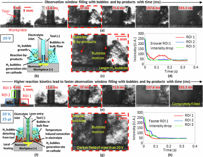
a With ECM the bubbles and by-products accumulate overtime with the b illustrated mechanism and c magnified view showing upward H2 bubble flow along tool. e With LECM the field of view (FOV) becomes darker quickly with accumulation of bubbles and by-products due to faster reaction kinetics with the f illustrated mechanism and g magnified view showing smaller bubbles than with c ECM. The intensity variation shows faster region of interest (ROI) 1 drop with h LECM than d ECM.
Passivation behaviour of rolled and SLMed samples
To investigate and validate the influence of sample manufacturing process and porosity on passivation as observed in the different current and pulse duration indicators of rolled and SLMed samples (Fig. 3m–p), we employed linear sweep voltammetry (LSV) using pin samples. Figure 6a, b shows the variation in current density and its decadic logarithm with voltage sweep, respectively with relevant process regimes indicated. The LSV results show that the SLMed sample was more reactive with a higher current density (0.05 A/cm2) in the passive regime than the rolled sample (0.03 A/cm2) and earlier onset of transpassive regime (4.9 V). This behaviour aligns with the corrosion behaviour study by Dai et al.40. They proposed that the acicular α’ microstructure that is generated due to high temperature gradients and rapid heating/cooling cycles during SLM, is a non-equilibrium microstructure and in a “higher energy state” towards corrosion. However, the current pulse analysis of ECM and LECM suggests that the SLMed samples were more resistant to EC-dissolution compared to rolled samples. This difference in behaviour is because the ECM conditions could not be generated during the LSV experiments as the logarithm of current density plateaued in the transpassive regime, indicating secondary passivation. Hence, the LSV experiments could not capture the actual passivation behaviour of the rolled and SLMed samples during ECM. Further, in our previous work14, we demonstrated that in highly passivating multiphase materials, the phase that is more electrochemically active absorbs more oxygen and preferentially passivates during ECM. Therefore, we conducted open circuit potential (OCP) experiments on pin samples subjected to ECM conditions (10 V for 5 s) for better understanding of the passive layer generated during ECM. The results in Fig. 6c validate the passivation mechanisms outlined by the current pulse analysis. The rolled sample had a stable passive layer whereas, the SLMed sample had higher OCP values (more resistive passivation) which continuously decreased due to passive layer corrosion/weakening at pore sites. This mechanism of preferential pore site dissolution is illustrated in Fig. 6d, which was observed by SEM images and also captured accurately by the current pulse analysis in Fig. 3. The schematic describes the mechanism through a simplified equivalent circuit to model the resistance of the electrolyte in interelectrode gap (Re), capacitance of the electrical double layer that is generated during ECM/LECM (Cd), Faradaic resistance (Rd), and the passive layer resistance and capacitance (R1, R2, C1, C2). These results affirm the need for ECM-specific measurement techniques (>15 V, >70 A/cm2) for evaluation of passivation and removal mechanisms during machining, since the potentiometric measurements are not always applicable and in some cases such as this, contradictory. The proposed current pulse analysis framework is a potential technique in this direction.

a Linear sweep voltammetry measurements and its b decadic logarithm showing SLMed sample is more reactive at low voltage/current density conditions (contradictory to behaviour during ECM). c Open circuit potential measurements showing the passive layer formed on SLMed sample after ECM is more resistant but unstable due to corrosion at pore sites, reflecting the actual behaviour during machining. d Illustration of passivation behaviour.
Investigation of Ti6Al4V passivation and removal behaviour during ECM and LECM
Cavity machining experiments (Figs. 7 and 9) were conducted at different time intervals to further investigate the passivation evolution during ECM and LECM in relation to the different processing conditions and material microstructure to support the conclusions inferred from the current pulse analysis framework in Fig. 3m–p. The results provided in Figs. 8 and 10, present the surface waviness analysis to study the evolution of crevices (preferential dissolution regions) and ridges (preferential passivation regions). We used the areal parameters of surface waviness (Wa) and Wdr (percentage of texture compared to planar surface) to analyse the surface morphology in both vertical and lateral directions. The cavities on the rolled samples had indications of stray machining around the contours of the cavities with poor circularity (Fig. 7a–i) as tool rotation was not employed. It is possible to machine cavities on Ti6Al4V with good circularity with tool rotation with NaNO3 electrolyte as shown in the supplementary information S1. However, the objective of this study was to analyse the passivation behaviour and not precise machining therefore, passivation favourable conditions were created and other process parameters except voltage and time were kept constant for repeatable results.

The SEM micrographs (50x) of cavities machined with a–e ECM and f–i LECM along with j methodology for k cavity profiles. The cavities enlarge over time and the higher transpassive dissolution kinetics with LECM lead to deeper cavities.

The 3D view of surface waviness in a section of the cavity machined with a–e ECM and f–i LECM along with j methodology for k waviness analysis (error bars of standard deviation of 4 measurements). With both a–e ECM and f–i LECM the crevice sites form at weaker passivated sites and coalesce overtime to generate dissolution regions with passivated ridges as quantified by increasing k Wa and Wdr. h, i Passivation weakening is better with LECM which improves crevice/ridge levelling as indicated by lower k Wa and Wdr.
The cavities on the rolled samples grew in size as time progressed (Fig. 7a–c, f–h). The cavity with 20 V ECM (Fig. 7c) was shallow with a large undissolved central hill (Fig. 7k) due to poor passivation weakening capability. The central hill or ‘w-shaped’ cavity is formed because with ECM the current density is low in the central hollow tool section. With 30 V ECM, the cavity became deeper and wide due to increased transpassive dissolution (Fig. 7d, k). With ECM at 40 V, the increased passivation induced by excessive intermittent joule heating led to a more localised cavity (Fig. 7e). The use of laser assistance improved passivation weakening and transpassive dissolution, leading to deeper cavities (Fig. 7h, i, k). Since LECM heats the workpiece surface in the central region, it weakens passivation and focuses the current density in the central tool region which improves removal localisation. However, the central hill could not be removed completely as a passivating electrolyte was used and by-products accumulation in the interelectrode gap increased due to enhanced transpassive dissolution with LECM, which increased laser attenuation. The passivation evolution investigation through surface waviness (Fig. 8) with different processing conditions and machining times can be described as following:
-
i.
At 1 s the surface indicated initiation of crevice and ridge formation (Fig. 8a, f). The crevices and ridges with LECM at 20 V were more evenly distributed and the ridges were smaller due to better passivation weakening capability. This was reflected in the 40% higher Wdr compared to ECM at 20 V (Fig. 8k).
-
ii.
At 4 s the crevice dissolution increased, leading to coalescence to form larger crevices (Fig. 8b, g). With LECM at 20 V, the better passivation weakening generated discontinuous ridges leading to higher Wa (13% higher) and Wdr (64% higher) values compared to ECM at 20 V (Fig. 8k).
-
iii.
At 10 s the preferential crevice dissolution and preferential ridge passivation became apparent (increase in Wa) and the difference in machinability was high with ECM at 20 V (Fig. 8c), resulting in the highest Wa (4.06 µm) and Wdr (9.1%) values (Fig. 8k). With LECM at 20 V (Fig. 8h), the passivation weakening was concentrated at crevice sites leading to crevice widening/ridge narrowing as reflected in the 13% lower in Wdr compared to ECM at 20 V. With ECM at 30 V (Fig. 8d), the preferential crevice removal remained but the passivation at ridges weakened slightly, leading to reduction in Wa and Wdr. LECM at 30 V (Fig. 8i), improved passivation weakening at ridges as the current density increase due to laser heating focusses at the protruding ridges, which improved ridge/crevice levelling as demonstrated by the lowest Wa of 3.1 µm. The Wdr was 15% lower than LECM at 20 V since the machinability difference in crevice and ridge sites was reduced. The higher passivation with ECM at 40 V due to unstable interelectrode gap conditions could be observed by the growth in passivated ridge sites (Fig. 8e) with similar Wa (3.4 µm) and Wdr (7.8%) values as ECM at 30 V.
The cavities on the SLMed samples were irregular (Fig. 9a–i) and considerably rougher (Fig. 9k) due to the higher unmachined sample roughness (Sa of 6.9 ± 0.3 µm), porosity induced inhomogeneous material dissolution and EC-dissolution resistant martensitic microstructure. The machining time of 10 s was insufficient to achieve a defined cavity with ECM at 20 V (Fig. 9c). However, at 20 V with LECM a defined cavity, although irregular could be observed. Similarly, the cavities with ECM and LECM at 30 V (Fig. 9d, i) were defined and deep, but with ECM at 40 V (Fig. 9e) the cavity became irregular again with a wide central hill due to high passivation caused by unstable interelectrode gap conditions induced by intermittent joule heating. All the cavities had large central hills even with LECM (Fig. 9k), since the least resistance current path was affected more by pore sites rather than the tool or laser. The passivation evolution and porosity influence in correlation to surface waviness (Fig. 10) can be described as following:
-
i.
At 1 s the crevice and ridge formation initiation could be observed on the surface (Fig. 10a, f). The crevices were slightly wider with LECM at 20 V as also indicated by the 14% lower Wdr value compared to ECM at 20 V (Fig. 10k).
-
ii.
At 4 s, similar to the rolled samples, the crevice dissolution increased to coalesce into larger crevices (Fig. 10b, g). With LECM at 20 V (Fig. 10g) the better passivation weakening reduced ridge growth/formation as evident by the considerably lower Wa (47% lower) and Wdr (56% lower) values compared to ECM at 20 V (Fig. 10k). However, it is also possible that with higher transpassive dissolution with LECM, more un-passivated/smoothened pore sites were present leading to lower Wa and Wdr.
-
iii.
At 10 s the difference in crevice and ridge machinability became obvious due preferential dissolution in pore sites (crevices). ECM at 20 V (Fig. 10c) did not follow the Wa (Fig. 10k) increasing trend with time of the rolled samples (Fig. 8k), as it had poor passivation weakening capability and had high porosity influence. With LECM at 20 V (Fig. 10h), the indications of preferential pore dissolution were observed by crevice deepening and widening, along with corresponding increase in Wa and Wdr to 14.5 µm and 132.8%, respectively (Fig. 10k). Similarly, with ECM at 30 V (Fig. 10d) the passivation weakening improved but porosity influence remained, leading to a 45% higher Wa and 52% higher Wdr than ECM at 20 V (Fig. 10k). The current focussing effect of LECM at 30 V (Fig. 10i) improved ridge and crevice levelling, but it was not as pronounced as the rolled samples as some porosity influence remained. This reduced Wa to 8.8 µm and Wdr to 58% (Fig. 10k). The higher passivation conditions with ECM at 40 V (Fig. 10e) led to re-passivation of even pore sites which reduced preferential pore site (crevice) dissolution as indicated by the low Wa (7 µm) and Wdr (37.6%) values (Fig. 10k).

The SEM micrographs (50x) of cavities machined with a–e ECM and f–i LECM along with j methodology for k cavity profiles. The cavities are rough and irregular due to preferential dissolution of un-passivated exposed pore sites.

The 3D view of surface waviness in a section of the cavity machined with a–e ECM and f–i LECM along with j methodology for k waviness analysis (error bars of standard deviation of 4 measurements). With both a–c ECM and f–i LECM the crevice sites form at pore sites and coalesce overtime to generate dissolution regions with passivated ridges as quantified by increasing k Wa and Wdr. c With ECM at 20 V there is possible high porosity influence and limited passivation weakening k decrease in Wa). h, i Passivation weakening at ridge sites is better and porosity influence is reduced with LECM which improves crevice/ridge levelling k lower Wa and Wdr).
The above results strongly support the passivation evolution mechanisms proposed through the current pulse analysis framework.
Discussion
The schematic in Fig. 11a summarises the proposed passivation evolution mechanisms with different processing conditions and material microstructure in correlation to the current pulse analysis indicators and cavity dimensions (Fig. 11b), as investigated in this study. In addition, the summary of results at different processing conditions is provided in supplementary information S2.

a Proposed passivation evolution and material removal mechanisms for the rolled and SLMed samples during ECM and LECM in correlation to current pulse analysis. b Cavity dimensions showing removal localisation with LECM and smaller dimensions of the more corrosion-resistant SLMed sample. Error bars are of standard deviation of 4 measurements. c Qualitative representation of processing windows. The sample current pulses of d Inconel 718 and e nitinol.
For the case of rolled samples, the surface experiences preferential dissolution at regions of weaker/weakened passivation to generate crevice sites and passivated ridge sites. With ECM, the preferential crevice dissolution is high due to poor passivation weakening capability. Overtime the machined surface is re-passivated due to the highly passivating nature of Ti6Al4V. This behaviour is reflected in the current pulse analysis, where tRON and tOFF’ states are observed as a consequence of high passivation resistance, which reduces the actual effective machining duration. During LECM, the laser locally heats the workpiece surface and increases the local electrolyte conductivity, leading to enhanced transpassive dissolution kinetics and current density increase. The higher current density gets focussed at the protruding/sharp ridge sites to weaken passivation and reduce the preferential crevice dissolution which improves uniform material dissolution. The improved passivation weakening capability increases the actual effective machining time as reflected in fewer tRON states and absence of tOFF states.
For the case of SLMed sample, the surface experiences preferential dissolution at pore sites where un-passivated surface is exposed, leading to a more uneven crevice and ridge pattern. With ECM, the preferential dissolution at pore sites is pronounced as the un-passivated surface is more susceptible to ECM in comparison to the passivated ridges. As a result, the tOFF’ state does not occur since pore sites are continuously exposed and experience preferential dissolution. However, tRON states can be observed in the current pulse analysis due to the EC-dissolution-resistant martensitic microstructure (lower current) and high passivation, which interrupts effective machining. LECM reduces porosity influence as the enhanced passivation weakening capability reduces preferential pore site dissolution and even re-passivates the surface, which leads to higher current and more tRON states.
Based on the cavity dimensions in Fig. 11b, it can be concluded that the LECM process can improve process localisation by weakening passivation primarily in the centre of the cavity, leading to lower width and higher depth. This behaviour is more pronounced in the SLMed sample as the exposure of pore sites further focuses material removal in the depth direction. However, the martensitic microstructure is more corrosion-resistant which results in smaller cavities. The above discussion and findings of this study are qualitatively summarised in Fig. 11c.
In summary, we have successfully demonstrated an on-machine framework based on high frequency current pulse analysis for quantitatively capturing the part level operando passivation behaviour with process history i.e. overall passivation evolution and effective machining/non-machining duration. In addition, it can be tested on different materials to compile a database for devising a global passivation index which combines different material-specific indicators. As shown in the unfiltered sample current pulses (duty cycle 50%) recorded using the same current pulse acquisition system at 10 MHz sampling rate in Fig. 11d, e, the pulse shape and defined indicators are material dependent. For Inconel 718, the pulse during tON is relatively flat as it is a low passivating material, but it fluctuates significantly which is possibly caused by the breakout of Laves and δ phases41. For nitinol, the pulse drops slightly during the tON period possibly due to the initial overpotential and Ti passivation, which then flattens out as nickel can be easily dissolved42,43. Therefore, the proposed on-machine passivation analysis framework has the potential for fundamental mechanistic passivation investigations of different materials during ECM and its hybrid variants by devising suitable indicators. In addition, the quantified indicators provide part level passivation information with clean and useful data to optimise data storage and computing resources. These indicators convert the current pulse data into quantified interpretable passivation phenomenon occurring on the workpiece surface (information carrier) as a result of different process loads (ECM assisted by laser, purely ECM) as per the “process signature concept”44. This makes it relevant in component production scenarios and the framework can be further extended to support the development of data driven models, process optimisation and digital twin of the ECM/LECM machine-tool2 using the “Aachen approach” proposed by Bergs et al.45 for improving process intelligence (Fig. 1h).
Since this study is an initial step towards on-machine mechanism-informed process investigations at actual ECM and LECM conditions, further research is required towards advanced studies involving on-machine quantitative analysis using high frequency in-process current signals and also their implementation on the machine-tool to adapt to changes in passivation layer to prevent process instabilities. Specifically, implementation of the framework on the machine-tool for real-time process analysis and control, requires dedicated research beyond simply using edge computers for calculating the indicators in real-time. This requires synchronisation of the process, controller and machine-tool by holistically resolving and coupling their different time constants. ECM/LECM involves electrical time constant (ns to μs), the mechanical stages have mechanical time constant (ms) and the laser induced weakening of passivation layer involves thermal time constant (sub-ms to ms) as well as the latency of communication protocol (EtherCAT).
Methods
Laser-ECM process principle
The hybrid laser-ECM (LECM) process scheme is illustrated in Fig. 1a. In LECM, laser is used as a hybridisation energy source as its non-contact nature complements ECM processing to provide localised removal with good surface quality. In addition, there is no chipping during ECM unlike mechanical machining, which provides clear interelectrode gap conditions for convenient laser application at the workpiece surface. The LECM technique supplies the electrolyte and green laser (532 nm) coaxially and simultaneously through the tubular tool to the machining zone to apply the pulsed EC (µs) and laser (ns) process energies (Fig. 1a). This energy coupling approach is especially suitable for processing passivating materials as the laser first interacts with the surface passive layer to weaken it upon exiting the tool before affecting the bulk material. The ns pulsed green laser provides fast and localised heating to the workpiece surface which has minimal absorption in water (α = 0.0045 m−1)46 to minimise attenuation. The heat is then transmitted to the electrolyte in the interelectrode gap from the workpiece surface through convection and conduction mechanisms which ultimately increases the local electrolyte conductivity47. The increase in local temperature and electrolyte conductivity results in increase in current density as well as reduction in the activation energy for EC-dissolution to accelerate the reaction rate as governed by the Arrhenius relation. The escalation of current density facilitates passivation layer weakening according to the following macroscopic mechanisms based on our previous works14,31:
-
i.
Higher current density can overcome the resistive barrier to structurally weaken passivation.
-
ii.
It can remove material beneath the layer through the gaps and pores, leading to layer spalling and exfoliation.
The passivation weakening, increased current density and combined laser and ECM input in turn facilitate uniform removal of phases with different electrochemical potentials/surface energies in the matrix. In addition, the process parameters (laser energy, interelectrode gap, flow rate and pulse parameters) are selected for process energies synergy, clear interelectrode gap conditions and thermal management to avoid adverse laser heating effects like electrolyte boiling, plasma formation and ablation, which would otherwise compromise ECM performance. Therefore, the material processing still exhibits anodic dissolution footprints and preserves the material properties without generating thermal defects. Furthermore, as the laser heats the workpiece surface under the hollow tool section, it shifts the least resistance current path from the solid tool section towards the centre, which localises material removal and passivation weakening in the centre of the machining zone14. These aspects make LECM suitable for processing highly passivating and multiphase materials like Ti6Al4V in pH-neutral salt electrolytes. Therefore, in this study ECM and LECM experiments were conducted on Ti6Al4V to observe if the improvement in passivation weakening can be quantitatively captured with the proposed framework.
Experimental setup
The in-house built machine-tool setup for performing ECM and LECM is shown in Fig. 1a. This machine-tool is based on a gantry type frame and includes the LECM machine, electrolyte supply circuit and control system. The machine-tool features a nanosecond (ns) pulsed green laser source and a microsecond (µs) pulsed voltage source to provide the necessary process energies for conducting experiments in a machining cell using a tubular electrode. This electrode behaves both as an ECM tool and multimodal waveguide to coaxially supply the electrolyte and laser through it. The hollow tool electrode, shown in Fig. 1a, has an outer diameter (O.D.) of 1.2 mm, an inside diameter (I.D.) of 0.65 mm and an inner quartz capillary with a 0.35 mm hole. The laser source from Spectraphysics® VGEN-G-HE30 provides the green laser with specifications: 532 nm wavelength, avg. power 30 W, max. pulse energy 180 μJ and max. pulse frequency 1500 kHz. The laser is directed towards the tool inlet through a focusing lens (200 mm focal length, 50 µm spot size), and the inner quartz lining enhances the laser acceptance angle while protecting the inner tool surface from corrosion, which is crucial for internal reflection of the laser. With this laser coupling configuration and electrolyte flow (2.4 M NaNO3), a power loss of 23% was measured at the tool exit using a thermopile sensor (L50 (150) A-BB-35) from Ophir®. The motion along the z-axis is done by using a precise ball screw drive with a resolution of 0.1 μm and repeatability of ±0.2 μm, which enables the interelectrode gap setting to less than 200 μm with the electrical touch method. The machining trajectory control along the x and y axes is achieved through a Standa® 8MTL120XY-planar XY linear motor direct drive stage, which offers an accuracy of ±0.5 μm and a repeatability of ±0.15 μm. The machine-tool is controlled through a LabVIEW® program deployed on a NI® cRIO-9045 controller and the LUMS® software to synchronize process energies and machine motion.
Sample microstructure
The microstructures of the samples were observed using the Philips® XL30 FEG scanning electron microscope (SEM). The microstructure was analysed after grinding the samples with grinding paper of 4000 grit size and 1 µm diamond paste with subsequent etching using a 50 ml H2O, 25 ml HNO3 and 5 ml HF solution. The SEM images in Fig. 1d indicate that the rolled sample had a microstructure with equiaxed α phase with β phase whereas, the as-built SLMed sample had mostly an acicular α’ martensitic microstructure as also previously observed by Vrancken et al.18.
Sample preparation
We used the Ti6Al4V rolled and SLMed samples in this study to assess the influence of microstructure and manufacturing process on the passivation and removal behaviour. The Grade 5 rolled samples were acquired from CASEO®. The SLMed samples were prepared from the extra-low interstitial Ti6Al4V powder from Raymore industries® by using the custom Mlab-2410312021 SLM machine with process parameters and scan strategy mentioned in Table 148. The samples of both materials were cut into 20 × 20 × 5 mm square samples by using the GF® Cut E 600 wire-EDM machine (Fig. 12a, b). The as-built SLMed samples were used in this study to also analyse the porosity influence on passivation and material removal. As a consequence of this choice, the SLMed sample was considerably rougher with Sa of 6.9 ± 0.3 µm (L-filter 25 µm, S-filter 2.5 µm) than the rolled sample (Fig. 12a) (Sa of 0.9 ± 0.03 µm) with unfused powder visible on the surface as shown in inset of Fig. 12b.

a Rolled sample (Sa of 0.9 ± 0.03 µm), b rough SLMed sample (Sa of 6.9 ± 0.3 µm) and c glass sandwiched sample for high-speed interelectrode gap camera observations.
Furthermore, for high-speed camera observations, the rolled samples were sandwiched between borosilicate glass plates to machine along the 20 × 5 mm surface and constrain the electrolyte flow (Fig. 12c). For the linear sweep voltammetry (LSV) and open circuit potential (OCP) experiments, pin samples of both materials with cross-section of 0.8 × 0.8 mm were prepared by using wire-EDM.
Machining approach
The ECM and LECM point drilling experiments were conducted at different process parameters with a machining time of 10 s to facilitate the passivation analysis. In addition, experiments were conducted at different machining times to investigate and validate the material passivation and removal mechanisms. Cavities were machined as test features without tool feed on rolled and SLMed Ti6Al4V samples (Fig. 12a, b) with parametric process parameters listed in Table 2. All the experiments were performed in 200 g/l (2.4 M) aqueous NaNO3 electrolyte (105 mS/cm at 20 °C) to create passivating machining conditions necessary for the passivation analysis. The samples were cleaned in an ultrasonic bath of de-ionized (DI) water (8 MΩ.cm) for 20 mins after machining before further characterisation and studies. All the samples were cleaned in the same batch to minimise sample handling associated modification of passive layer and EDS measurement errors.
Current pulse acquisition
The schematic for the current pulse acquisition is shown in Fig. 1b. The current pulse signal is acquired through the Digilent® Analog Discovery 2 digital oscilloscope (voltage: ±25 V, max. sampling rate: 100 MHz, bandwidth: 30 MHz) by using a Hall sensor installed on the electrical circuit of the machine-tool setup. The digitized current pulse data is transferred to a separate workstation through the NI® cRIO-9045 controller for analysis using a Matlab® script. For acquiring the current pulse signal, a sampling rate of 10 MHz was set as 100 times higher than the voltage pulse width of 10 µs to accurately measure the pulse drop and fluctuations within the pulse-ON duration.
Calculation of framework indicators
For calculating pulse duration indicators (Fig. 2a), data counting approach was applied as the designed pulse-ON condition (tON) and designed pulse-OFF condition (tOFF) were both set as 10 µs, along with current values to detect tON’, tRON and tOFF’ states. For calculating current indicators (Fig. 2a), the thresholding approach was applied. The tOFF condition was filtered out by using a threshold of 0.2 A. Based on these indicators the pulses were classified into normal, reduced and OFF’ pulse types for subsequent statistical analysis of the indicators. The framework extracted information from the raw digitized current pulse data to generate separate datasets for each pulse type to reduce computation time (~1 min for 10 s machining duration). The tOFF condition was also removed during the statistical analysis of pulse duration indicators to improve computation time as no material processing occurs during this period.
Sample density and porosity measurements
The density of the rolled and SLMed samples were measured through the Archimedes density method using the following equation with ethanol as the immersion liquid:
The average density of the samples listed in Table 3 was calculated after measuring 20 samples. The SLMed samples had a 0.485% lower density than the rolled samples due to porosities. In addition, the SLMed sample porosity was analysed through a computed tomography (CT) scan. The CT scan in Fig. 13 shows that the SLMed samples had porosities throughout the sample with different diameters and a defect volume ratio of 0.16% as a consequence of the SLM process parameters and scan strategy.

a Computed tomography scan of the sample showing porosity and b frequency distribution of measured porosity.
Potentiometric measurements
The Gamry Instruments Reference 600+ potentiostat which has a max voltage of ± 11 V and max current of ±600 mA, was used to perform the linear sweep voltammetry and open circuit potential experiments. The rolled and SLMed Ti6Al4V pin samples were used as the working electrodes, a platinum wire as the counter electrode and a Sigma Aldrich® silver/silver chloride (Ag/AgCl) electrode as the reference electrode with 2.4 M NaNO3 electrolyte added into a glass beaker. For the linear sweep voltammetry experiment, a voltage sweep of −4 V to 7 V was applied to the clean pin samples to observe the different electrochemical process regimes and influence of the sample microstructure and porosity with a scan step of 1 mV and scan rate of 100 mV/s. For the OCP experiments, pin samples were first subjected to ECM in a two-electrode beaker setup using the LECM setup voltage source (Elecktro-Automatik® PS 2084-10B, max. voltage 84 V, max. current 10 A) with 10 V applied for 5 s in 2.4 M NaNO3 electrolyte, and used without cleaning to study the stability/corrosion resistance of the passive layer generated during ECM along with the influence of sample microstructure and porosity on it. The total time was set as 600 s with sampling period of 0.5 s for the open circuit potential experiments.
High-speed camera observations
To facilitate real-time observation of the ECM and LECM processes, a specialized setup was developed, as shown in Fig. 14. This setup included a Photron® SA3 high-speed camera with a Nikon® NIKKOR 105 mm macro lens along with Tamron® N-AFD teleconverters (2) and three extension tubes. In addition, a high-pass interferometric filter was placed in front of the camera lens to eliminate laser contributions from the observations during LECM experiments. The camera unit was mounted on a vibration-free flat platform from Thorlabs®. The camera observations were made using a shutter time of 0.33 ms and framerate of 3000 fps. An image processing code in Matlab® was used to analyse intensity variations to indicate by-product/bubble generation over time, within defined regions of interest (ROIs). For intensity measurements in the selected ROIs (Fig. 5e), an image of the ROI before machining (clear) was subtracted from each image (background removal), and then the intensity levels in the ROIs were averaged. This background removal enhanced contrast and increased the signal-to-noise (S/N) ratio. No further post-processing were done on the images. Visualization was performed near the interelectrode gap, using three LED lights and a red pilot laser to ensure adequate illumination and avoid image flickering during observations. An interface developed in the NI LabVIEW® program enabled simultaneous initiation of the process (laser and ECM) and camera recording via an external 5 V TTL trigger.

Schematic of the custom setup for high-speed interelectrode gap camera observations during ECM and LECM. The custom setup configuration and associated components.
Dimension and profile measurements
The Sensofar® S Neox 3D optical microscope was used to measure the cavity dimensions and extract the profile. The cavity point cloud was measured by stitching together 4 field of views (FOVs) obtained by the 20x objective with 15% overlap. Two cavity profiles were extracted along the X and Y axes for each cavity along its centre (Figs. 7j and 9j). Thereafter, the depth and width were measured along the profile to obtain 2 measurements per cavity, for a total of 4 measurements per processing conditions. These 4 measurements were used to compute the average values and standard deviations for the error bars in Fig. 11b.
Surface waviness measurements
The Sensofar® S Neox 3D optical microscope was used to analyse the waviness evolution of the cleaned samples after machining with different time periods and process parameters. A scan area of 300 × 300 µm was used centred at the deepest cavity region as shown in Figs. 8j and 10j for an objective comparison between the rolled and SLMed samples as well as the processing conditions. A 20x objective with green light was used for observation. In order to extract surface waviness a form filter of 3rd order polynomial was applied to remove the form and a L-filter of 25 µm was applied to remove roughness features. A total of 4 measurements were taken per processing condition (2 measurements per cavity) to compute the average values and standard deviations for the error bars in Figs. 8k and 10k.
Passivation analysis and sample characterisation via metallography
The machined samples after cleaning were observed using a Philips® XL30 FEG scanning electron microscope (SEM) to characterise the surface and passivation. A scan area of 50 × 50 µm was used to perform energy dispersive X-ray spectroscopy (EDS) to quantify the oxygen wt% on the surface using the EDAX® TEAM software by taking 3 measurements. The scan area was centred at the ridge/crevice boundary to have similar observation windows for all the machined samples.


Responses