Advanced 3D printing accelerates electromagnetic wave absorption from ceramic materials to structures

Introduction
As radar technology advances and the application of electromagnetic waves (EMW) become more prevalent, the issue of electromagnetic pollution has become increasingly pressing. Therefore, it is crucial to develop innovative materials for electromagnetic wave absorption (EMWA) to mitigate electromagnetic interference across military, industrial, and residential environments1,2,3. While various materials such as ferrite4,5,6 and carbon-based7,8 materials are used for EMWA, it is the ceramic materials that have recently captured significant attention due to their unique combination of chemical stability, lightweight, high-temperature resistance, and high strength9,10,11,12.
Traditional fabrication methods for ceramic materials, while effective, still be time-consuming and may struggle to produce complex structures13,14. The advent of 3D printing technologies has revolutionized this field by enabling the creation of complex geometries and structures15,16,17, which are essential for the next generation of EMWA designs. Traditionally, the preparation of ceramic materials for EMWA has focused on the design of material composition (adjusting the type and proportion of dielectric materials) and microstructure (such as hollow, core-shell, and graded structures). Advanced 3D printing has facilitated a transition from ceramic material-centric to ceramic structure-centric design in EMWA, allowing for the development of advanced structures that enhance absorption capabilities. This technology enables the integration of material composition and structure during the design phase, achieving collaborative optimization of materials and structures. Advanced 3D printing technologies provide efficient approaches to producing the complex, unconventional structures required for advanced ceramic materials for EMWA. The application of 3D printing technologies to ceramic materials has seen significant growth, with various techniques now available for fabricating these materials.
The research focus has increasingly shifted toward understanding the intricate electromagnetic properties of these 3D-printed ceramic materials and structures for EMWA, as shown in Fig. 1. 3D-printed ceramic materials for EMWA can be broadly categorized into two types: pristine ceramics (precursor-derived ceramics (PDCs) and powder-based ceramics) and ceramic-based composites (carbon/ceramic composites, ceramic/ceramic composites, and metal/ceramic composites). 3D-printed ceramic structures for EMWA can also be broadly categorized into seven types: porous structures, honeycomb structures, stepped structures, twisted cross structures, triple periodic minimal surface (TMPS) structures, pyramid structures, and lattice structures. Given the expansive research in the field and the multitude of 3D-printed ceramic materials and structures, there is a notable absence of a comprehensive review that consolidates these advancements.

Advanced 3D printing accelerates EMWA from ceramic materials to structures.
Herein, the acceleration of electromagnetic wave absorption from ceramic materials to ceramic structures by advanced 3D printing was reviewed, which includes comparisons of different types of ceramic materials, as well as the applications of 3D printing technologies in them. Furthermore, the current limitations and future development tendency of 3D-printed ceramic materials and ceramic structures for EMWA were concluded. It is believed that the application of 3D printing technology in the field of ceramic materials and structures for EMWA is of great significance, and the research is anticipated to reciprocally foster advancements in 3D printing technology.
Advanced 3D printing technologies
The 3D printing technologies applied to fabricate ceramic materials and structures for EMWA can be categorized into four main types: vat photopolymerization (VPP), powder bed fusion (PBF), binder jetting (BJT), and material extrusion (MEX), as shown in Fig. 2.
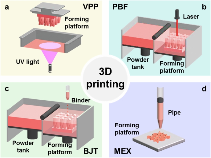
a vat photopolymerization (VPP), b powder bed fusion (PBF), c binder jetting (BJT), and d material extrusion (MEX).
Vat photopolymerization
VPP is a 3D printing technology that utilizes a specific wavelength of light to solidify photosensitive slurries into a three-dimensional structure, as depicted in Fig. 2a. The creation of ceramic-based photosensitive slurries can be accomplished through two methods: (1) by modifying the precursor ceramic polymer to enable photocuring capabilities18,19; (2) by mixing the precursor ceramic polymer or ceramic powders into photosensitive resins20,21. This technique is renowned for its high precision and resolution in printing, making it particularly well-suited for the fabrication of intricately shaped, small-scale ceramic components. However, it is important to note that the VPP-fabricated pre-ceramic components require a pyrolysis process to transform into final ceramic components. Pyrolysis results in significant volume shrinkage, which has a direct impact on the dimensional accuracy of the finished components22. This shrinkage must be carefully accounted for during the design and manufacturing process to ensure the components meet the required specifications.
Powder bed fusion
PBF is another 3D printing technology that constructs components layer by layer by selectively melting powders with laser beams, as shown in Fig. 2b. The resolution of ceramic components fabricated by PBF is determined by the particle size of powders and the precision of the laser23,24,25. This technology can directly use ceramic powders as raw materials. However, the direct manufacturing of dense ceramic components through PBF remains a challenge. It requires careful control of laser energy to achieve the necessary melting and sintering of the ceramic powders, avoiding excessive shrinkage or deformation26. Additionally, the issue of residual stress in PBF-fabricated ceramic components is another problem that needs to be addressed27.
Binder jetting
BJT technology involves spraying adhesive onto a powder bed, selectively bonding powders together to form three-dimensional components, as illustrated in Fig. 2c. The advantage of BJT is its ability to efficiently and batch print ceramic components with complex shapes28,29,30. Different from PBF, BJT operates without the need to melt a powder bed, which eliminates the generation of residual stresses. Fabricating ceramic components using BJT presents challenges due to the morphology of ceramic powder and the need for post-processing. The densification of these components is difficult because of the inherent porosity and large particle size of the powders. To address these issues, spray freeze drying has been applied to ceramic powder to prepare granules from angular powders, thereby improving powder flowability and sinterability31,32.
Material extrusion
MEX is a widely used 3D printing technology that functions by extruding semi-fluid materials through a printing nozzle. These materials are then sequentially solidified to construct three-dimensional components, as shown in Fig. 2d. Ceramic powders, precursor ceramic polymer, and ceramic fibers can be used as raw materials for the preparation of slurries suitable for MEX. This technology shows a great prospect in the fabrication of continuous fiber-reinforced ceramic matrix composites33,34,35. While ME is known for its ease of operation, it does have some limitations, including lower resolution and restrictions on printable structures. To overcome these challenges, advancements in MEX technology have been explored, such as UV-assisted MEX36,37 and embedded MEX38,39. These advancements enhance the solidification process to improve the resolution and expand the capabilities of MEX for more complex structure fabrication.
3D-printed ceramic materials for EMWA
When designing and evaluating materials for EMWA, dielectric constant, magnetic permeability, and loss tangent are key characteristics. Materials with high dielectric constant can polarize and store electromagnetic energy more effectively, while materials with high magnetic permeability can enhance magnetic loss, both of which together improve absorption capacity. The loss tangent measures the efficiency of a material in converting electromagnetic energy into thermal energy, and the higher its value, the stronger the material’s EMWA performance. These characteristics directly affect the application effectiveness of materials in fields such as electronic devices, aerospace, and military stealth. 3D-printed ceramic materials for EMWA can be broadly categorized into two types: pristine ceramics and ceramic matrix composites. Pristine ceramics, which are primarily dielectric loss-type absorbing materials, function through energy dissipation during the dipole polarization relaxation process40,41. On the other hand, ceramic matrix composites integrated contain electrical loss-type or magnetic loss-type42,43 EMW absorbing materials within a ceramic matrix. These composites leverage the complementary properties of magnetic and dielectric materials to modulate electromagnetic parameters and subsequently enhance EMW absorbing properties.
Pristine ceramics
The PDCs and ceramic powder are common raw materials for 3D-printed pristine ceramic EMW absorbers.
Precursor derived ceramics
PDCs are important raw materials for 3D-printed ceramic materials for EMWA, leveraging the combined benefits of polymer processability and ceramic properties. The flexibility of PDC molecular design makes it exceptionally suitable for VPP-based 3D printing technologies44. By introducing photocuring groups (such as acrylate groups, unsaturated double bond groups, and click-base sulfhydryl groups) into the precursor molecules, these materials acquire photocuring ability45,46. This advancement has garnered significant interest as it enables the fabrication of high-performance ceramics with refined structures through VPP-based 3D printing, and the development of the customization and optimization of ceramic materials for EMWA. Some researchers successfully conducted research on VPP-fabricated PDCs for EMWA, such as SiOC, SiCN, and SiBCN.
SiOC has the advantages of high chemical stability, thermal stability, tailorable structure, and a wide range of sources47,48,49. Feng et al.47 used methyl-phenyl silicone resin as the SiOC precursor and added the photo-absorber (E133). Then VPP-based 3D printing was used to fabricate the SiOC ceramics. The SiOC green bodies demonstrated high precision and maintained the original design without significant deformation. After the pyrolysis, some limited loss of shape can be discerned by looking at the external surface of the SiOC. The impact of pyrolysis temperatures on the electromagnetic properties is illustrated in Fig. 3a–c. The SiOC ceramics pyrolyzed at 1200 °C, when the thickness was 1.58 mm, the minimum reflection loss (RLmin) and the effective absorption bandwidth (EAB) were −23.5 dB and 4.9 GHz, respectively. Based on the above study, Zhou et al.50 proposed a novel ultraviolet-curable polysiloxane (PSO) precursor for VPP-based 3D printing. The PSO was modified by two different unsaturated double bonds to achieve a higher ceramic yield along with an efficient light-curing property. Following pyrolysis at 1200 °C, the 3D-printed SiOC structures remained crack-free and retained their shape, attributed to a consistent linear shrinkage of 34.7%.
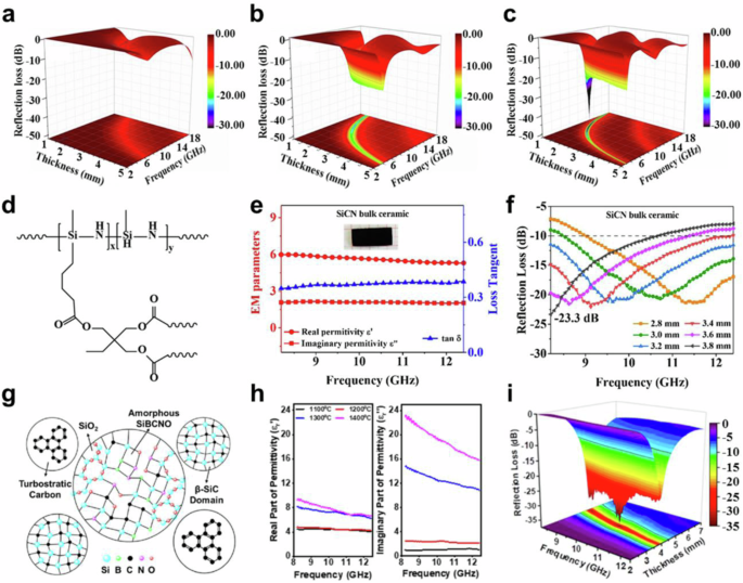
The reflection loss of SiOC ceramics pyrolyzed at a 1100 °C, b 1200 °C, and c 1300 °C47, d co-photopolymerization between acrylate groups and vinyl groups in PSZ53, e the electromagnetic parameters and f the reflection loss of the bulk SiCN ceramics53, g schematic illustration of the microstructure of SiBCN(O) ceramics55, h the electromagnetic parameters, and i the reflection loss of SiBCN(O) ceramics55.
SiCN ceramics are renowned for their exceptional hardness, thermal conductivity, and oxidation resistance. These properties, coupled with the ability to fine-tune their dielectric and magnetic properties, make SiCN ceramics highly desirable for high-temperature applications and advanced electromagnetic systems51,52. Recent studies have shown that SiCN ceramics have been successfully integrated into the field of 3D-printed PDCs for EMWA. While polysilazane (PSZ) serves as the primary precursor for SiCN ceramics, it lacks inherent photocuring properties. In contrast to the direct modification of SiOC precursor, PSZ is usually mixed with photosensitive resin to prepare a photocurable slurry suitable for VPP-based 3D printing. Pan et al.53 prepared photocurable slurries by mixing PSZ with acrylate photosensitive resins, enabling the 3D printing of green bodies via VPP-based 3D printing. They also adjusted the mixing ratio of PSZ and acrylate photosensitive resins to achieve high-performance 3D-printed SiCN ceramics (as depicted in Fig. 3d), the obtained structures showed delicate features and were well preserved after pyrolysis. The real permittivity (ε’) and the imaginary permittivity (ε”) of the bulk SiCN ceramics were in the range of 5.30–5.98 and 2.00–2.15, respectively, as shown in Fig. 3e. The obtained SiCN bulk ceramics could have an RLmin of −23.3 dB at a thickness of 3.8 mm and an EAB of 4.2 GHz at a thickness of 3.2 mm, as illustrated in Fig. 3f.
SiBCN ceramics, derived from polyborosilazane (PBSZ), maintain an amorphous state and resist crystallization up to 1700 °C, endowing them with exceptional phase stability. Consequently, these materials exhibit not only superior thermal stability but also remarkable resistance to high-temperature oxidation54. Xu et al.55 developed a novel photocurable PBSZ suitable for VPP-based 3D printing via a straightforward aminolysis method. First, an aminolysis reaction between chlorosilanes and amines formed the polyborosilazane backbone, and the incorporation of 2-hydroxyethyl acrylate (HEA) conferred photosensitivity to the PBSZ. Additionally, phenyl-substituted chlorosilanes were utilized to stabilize the B-N units within the polymer chain and to finely control the carbon content in the obtained SiBCN ceramic. These modifications to PBSZ enabled a stable 3D printing process, allowing for the creation of complex structures with high precision and reliability. Figure 3g shows the schematic illustration of the microstructure of SiBCN(O) ceramics. The effects of pyrolysis temperature on the dielectric properties were also investigated, as depicted in Fig. 3h. The SiBCN ceramics pyrolyzed at 1200 °C showed excellent EMW absorbing properties with an RLmin of −36.68 dB and an EAB of 4 GHz (covering the entire X-band) at a thickness of 3.7 mm, as depicted in Fig. 3i.
Powder based ceramics
Currently, some researchers have also turned attention to using ceramic powders as raw materials for 3D printing. Considering the low ceramic yield of PDCs, ceramic powders are generally less expensive, especially for large-scale production, which can reduce overall production costs.
SiC powders are highly promising raw materials for broadband and high-temperature EMWA, due to their exceptional characteristics, such as anti-oxidation properties, high hardness, and excellent wear resistance56,57. Zhou et al.58 mixed the SiC powders with photosensitive resin to prepare a photocurable slurry suitable for VPP-based 3D printing. Then precursor infiltration and pyrolysis (PIP) process was conducted to obtain dense SiC ceramics. Their study demonstrated that the obtained SiC ceramics maintained effective EMW absorbing properties across a wide temperature range, with stable complex permittivity (as shown in Fig. 4a, b) and high dielectric loss tangent (as shown in Fig. 4c), making them suitable for high-temperature EMWA applications. Wang et al.59 fabricated a SiC slurry by mixing SiC powders and distilled water and chose water-based MEX-based 3D printing to fabricate SiC green bodies. The use of a high solid loading slurry with a small amount of polymer in the preparation was beneficial for large-scale fabrication. The real permittivity and imaginary permittivity of as-obtained SiC ceramic approached 10 and 2.3, respectively, within the frequency range of 2–18 GHz, as depicted in Fig. 4d, e. The obtained SiC ceramics showed good performance with an EAB of 3.34 GHz at a thickness of 1.5 mm, and an RLmin of −30.30 dB at a thickness of 4.5 mm, as illustrated in Fig. 4f.
a real part, b imaginary part, and c dielectric loss tangent of the complex permittivity of SiC ceramics printed by VPP at different temperatures58, d real part, e imaginary part, and f the reflection loss of SiC ceramics printed by MEX59.
Ceramic-based composites
To achieve enhanced EMWA performance, a common strategy is to fabricate ceramic-based composite materials with a variety of EMW absorbing materials. Currently, three main approaches are utilized to achieve 3D-printed ceramic-based composites: (1) some EMW absorbing materials can be easily mixed to prepare raw materials suitable for 3D printing; (2) other materials are introduced by a sintering process into the 3D-printed ceramic bodies, (3) the use of multi-material 3D printing techniques, which allow for the incorporation of various materials in a single structure. Some researchers have conducted research on 3D-printed ceramic-based composites for EMWA, such as carbon/ceramic composites, ceramic/ceramic composites, and metal/ceramic composites.
Carbon/ceramic composites
Carbon materials, such as carbon nanotubes (CNTs), graphene, pyrolytic carbon (PyC), and carbon fibers, are widely used for EMWA due to their lightweight, high specific surface area, adjustable dielectric performance, and environmental friendliness60. Among them, CNTs and graphene as carbon-based nanomaterials have garnered significant interest due to their excellent electronic conductivity and porous structure. You et al.61 developed a two-step process to fabricate SiC composites with a nanostructured network of CNTs and graphene nanoplatelets with Fe3O4 nanoparticles, as shown in Fig. 5a. A CNT/graphene/Fe3O4/polymer green body was fabricated via MEX-based 3D printing. Then SiC ceramics were introduced by chemical vapor deposition. The pyrolysis process of residual organic polymer built enough deposit sites and transmission channels, which ensured that the in situ-grown SiC could directly adhere to the surfaces of CNTs and graphene. The as-obtained CNT/graphene/Fe3O4/SiC composites possessed an RLmin of −48.7 dB at a thickness of 4.8 mm and an EAB of 4.3 GHz (11.5–15.8 GHz) at a thickness of 2 mm. The EMW absorbing properties could remain consistent after annealing at 400 °C for 4 h, as shown in Fig. 5b, c. Liu et al.62 employed a similar approach to prepare MoS2/PyC-Al2O3 composites. An Al2O3/photosensitive resin slurry was shaped into green bodies by VPP-based 3D printing, followed by a pressureless sintering process in an ambient atmosphere to remove the resin. Subsequently, a PyC layer was deposited onto Al2O3 ceramics through a PIP process. Finally, MoS2 was in situ grown on the surface of the PyC layer via a hydrothermal method, as shown in Fig. 5d. When the thickness was 3 mm, the PyC-Al2O3 composites exhibited enhanced EMW absorbing properties, with an EAB covering most of the X band (8.6–12.4 GHz) and an RLmin of −44.00 dB at the frequency of 10.1 GHz, as shown in Fig. 5e.
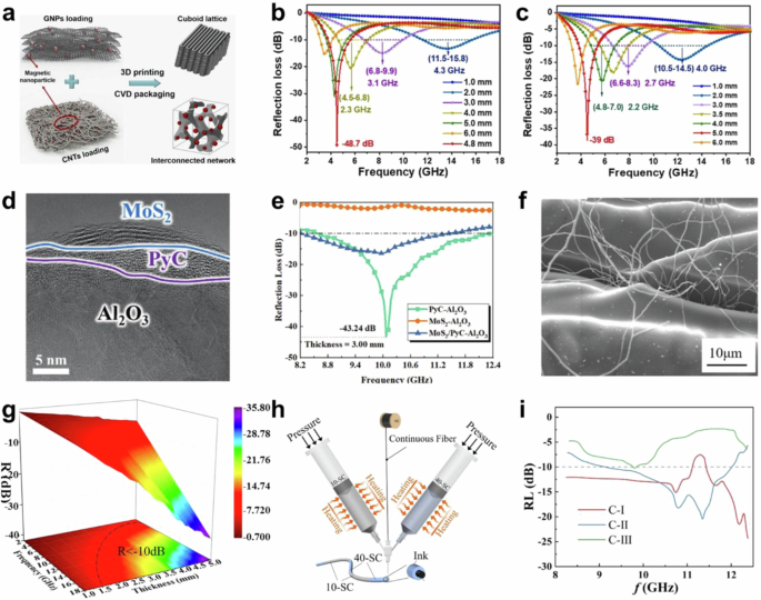
a Schematic illustration of the structural evolution in the preparation processes of CNT/graphene/Fe3O4/SiC composites61, the reflection loss of CNT/graphene/Fe3O4/SiC composites b before and c after 400 °C annealing61, d TEM image of MoS2/PyC-Al2O3 composites62, e the reflection loss of MoS2/PyC-Al2O3 composites62, f SEM image of carbon nanowires/FeSiOC composites after pyrolysis63, g the reflection loss of carbon nanowires/SiOC(Fe) composites63, h schematic diagram of dual MEX-3D printing64, i the reflection loss of Cf/SiC composites64.
Different from the above methods, Lin et al.63 introduced an innovative sintering technique featuring segmented slow heating and prolonged holding time. This process was utilized to enrich 3D-printed FeSiOC ceramics with carbon nanowires (Cnw) after pyrolysis, as illustrated in Fig. 5f. The Cnw/FeSiOC composites possessed an RLmin of −35.72 dB and an EAB of 12.7 GHz (5.3–18 GHz), when the thickness was 5 mm, as shown in Fig. 5g. Further expanding the horizons of 3D printing technology, Li et al.64 developed a novel dual MEX-3D printing to fabricate continuous carbon fiber/SiC (Cf/SiC) composites. During printing, the two slurries were alternately extruded, allowing the fabrication of gradient materials, as shown in Fig. 5h. The as-obtained Cf/SiC composites exhibited an RLmin of −24.3 dB and an EAB of 3.98 GHz, as illustrated in Fig. 5i. This work provided a controllable strategy for designing materials to achieve high-performance properties.
Ceramic/ceramic composites
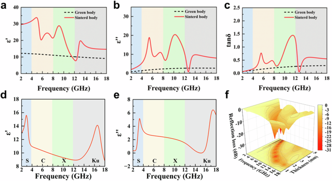
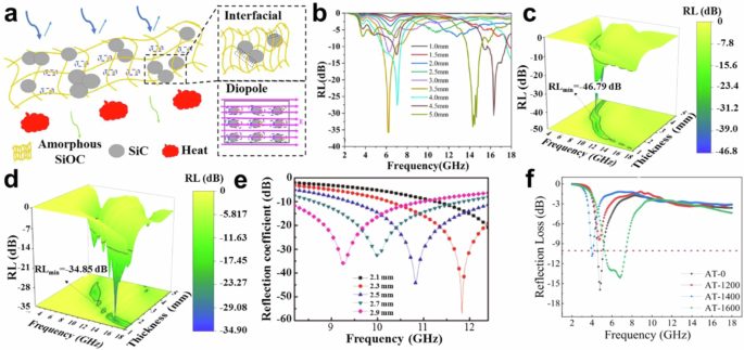
Presently, ceramic/ceramic composites contain two types: dual ceramic composites and ceramic fiber/ceramic composites. Dual ceramic composites are easily created by combining two ceramic materials into a slurry suitable for 3D printing. Miao et al.49 mixed liquid hydroxyl silicone oil and SiC powders to prepare a slurry suitable for MEX-based 3D printing. After sintering, SiC/SiOC composites without cracks could be obtained. The effects of the mass ratio of SiC to hydroxy silicone oil on the EMW absorbing properties were also investigated. The dielectric loss caused by added SiC enhanced the EMW absorbing properties, as shown in Fig. 6a. When the mass ratio of SiC to hydroxy silicone oil was 5:7, the composites with a thickness of 3.5 mm could achieve an RLmin of −36 dB and a corresponding EAB of 2 GHz, as depicted in Fig. 6b. An alternative approach is to incorporate the second ceramic through the sintering process. Yu et al.65 produced SiC/Si3N4 composites by PBF-based 3D printing for Si3N4 green body fabrication and PIP for SiC ceramic integration. The SiC/Si3N4 composites with a thickness of 2.4 mm after 4 cycles of PIP process had an RLmin of −46.79 dB, while the EAB was only 1.44 GHz, as illustrated in Fig. 6c. To enhance the impedance-matching properties and expand the EAB of SiC/Si3N4 composites, they applied infiltration treatment with Al2O3, TiO2, and Al(H2PO4)3 sols. Notably, as shown in Fig. 6d, the TiO2 infiltration treatment significantly improved the EAB to 4.08 GHz.
a polarization mechanism and b the reflection loss of SiC/SiOC composites49, c the reflection loss of SiC/Si3N4 composites after 4 PIP cycles65, d the reflection loss of SiC/Si3N4 composites with TiO2 infiltration65, e the reflection loss of SiCnw/Si3N4 composites after 3 PIP cycles66, f the reflection loss of SiCnw/Si3N4 composites with different annealing temperatures67.
As known, one-dimensional SiC nanowires (SiCnw) exhibit higher electrical conductivity, which contributes significantly to EMWA. The in situ growth of SiCnw is feasible through the pyrolysis of polycarbosilane (PCS) as a precursor. Duan et al.66 successfully combined 3D printing and the PIP process to fabricate SiCnw/Si3N4 composites. The 3D-printed Si3N4 green bodies featured high porosity, which accommodated the in situ growth of SiCnw. The incorporation of ferrocene during the PIP process facilitated the growth of SiCnw, with the quantity being controlled by the number of PIP cycles. Notably, the SiCnw/Si3N4 composites produced after 3 PIP cycles demonstrated enhanced EMW absorbing properties, achieving an RLmin of −57 dB at a thickness of 2.3 mm, as depicted in Fig. 6e. Yu et al.67 employed a similar strategy to fabricate SiCnw/Si3N4 composites, with a particular focus on the effect of annealing treatment on the microstructure and EMW absorbing properties. As the annealing temperature increased, the SiCnw morphology evolved from rod-like to stub-like, which led to a reduction in surface charge density and a consequent decrease in both the real and imaginary parts of the complex permittivity. When the annealing temperature reached 1600oC, the SiCnw/Si3N4 composites possessed an RLmin of −14.1 dB and an EAB of 2.16 GHz, as shown in Fig. 6f.
Metal/ceramic composites
Metal doping of ceramic-based composites can significantly optimize their EMW absorbing properties by altering the dielectric constant and magnetic permeability68. The incorporation of metal particles not only boosts the conductivity but also enhances the material’s capacity to absorb EMW, particularly in the high-frequency range.
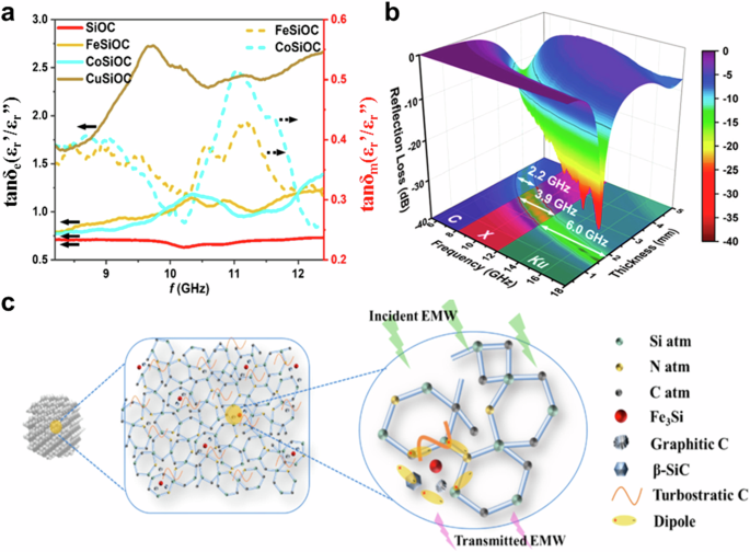
Advancements in 3D printing technology have further propelled the development of such materials for EMWA. Yao et al.69 added metals in the SiOC precursor to modify the electromagnetic parameters and 3D-printed FeSiOC, CoSiOC, and CuSiOC composites. The electromagnetic parameters of metal-doped SiOC ceramics were quite different compared to the pristine SiOC ceramics, as depicted in Fig. 7a. Metal-doped SiOC ceramics possessed a larger magnetic loss tangent. In summary, the advancements in 3D printing technology have significantly enhanced the development of SiOC ceramics for EMWA. Xing et al.70 mixed gallium indium alloy (EGaIn) nanoparticles with a photocurable ceramic precursor (PBS) to prepare a slurry suitable for VPP-based 3D printing. The low viscosity and high boiling point of EGaIn facilitated the maintenance of slurry fluidity during 3D printing and ensured stability throughout the pyrolysis process. As shown in Fig. 7b, the Si(GaIn)BOC composites achieve an EAB of 2.2 GHz (at a thickness of 3.4 mm) at C band (5.4–8.2 GHz), 3.9 GHz (at a thickness of 2.6 mm) at X band (8.2–12.4 GHZ), and 5.6 GHz (at a thickness of 1.9 mm) at Ku band (12.4–18 GHz), respectively. Feng et al.71 added the ferrocene into the PSZ and fabricated FeSiCN ceramics by VPP-based 3D printing. They found that the FeSiCN showed good performance with an EAB of 4.57 GHz at a thickness of 1.30 mm, and an RLmin of −61.34 dB at a thickness of 2.22 mm, when containing 0.5 wt % ferrocene. The introduction of ferrocene was beneficial for the in situ formation of a large amount of turbostratic carbon, graphite, and SiC nanosized phases, resulting in the increase of conductivity loss, as shown in Fig. 7c.
a The electromagnetic parameter of metal-doped SiOC composites69, b the reflection loss of Si(GaIn)BOC composites70, c schematic diagram of possible microwave radiation absorption mechanisms in the FeSiCN ceramics71.
In summary, as listed in Table 1, the evolution of advanced 3D printing technologies has significantly enhanced the development of ceramic materials for EMWA. The absorption properties of these materials are optimized by precisely controlling their microstructure and chemical composition. The incorporation of metal dopants or other functional components into ceramic-based materials not only enhances the electromagnetic wave loss mechanisms but also substantially improves their absorption efficiency and effective bandwidth within specific frequency ranges. However, bulk ceramic-based materials struggle to meet modern market and technology demands in terms of narrow absorption bandwidth (EAB < 5 GHz), due to limited structure designs and optimization.
3D-printed ceramic structures for EMWA
Generally, the attenuation of electromagnetic waves in materials can be enhanced in two ways. First, by increasing the material’s electromagnetic parameters such as the complex permittivity and permeability, which affect reflection and absorption. Second, the design of the material’s structure affects the propagation path of the electromagnetic waves. The greatest advantage of 3D printing technologies in the field of ceramic materials for EMWA is its ability to fabricate complex structures, meeting the demands for broad bandwidth, lightweight, strong absorption, and integrated multi-functionality. Currently, some researchers have concentrated on the 3D-printed ceramic structures for EMWA, offering innovative design strategies to further advance this field.
Porous structures
Porous structures are typical structures that can enhance the EMW absorbing properties by increasing the scattering and reflection of EMW within their internal cavities72,73,74. Some researchers have paid attention to 3D-printed ceramic-based porous structures. The utilization of naturally porous precursors is a common method to fabricate porous structures. Lv et al.75 fabricated SiC nanowires/SiC whiskers (SiCnw/SiCw) porous structures by BJT-based 3D printing combined with the PIP process. To address the poor flowability of SiCw for BJT-based 3D printing, SiCw spheres were prepared via spray drying. Subsequently, the porous SiCw structure was created using BJT, and SiCnw were in situ grown within this structure via PIP, resulting in the SiCnw/SiCw porous structure, as depicted in Fig. 8a. This porous structure exhibited an RLmin of −57 dB at a thickness of 2.68 mm and an EAB of 4 GHz at a thickness of 2.71 mm, as shown in Fig. 8b. Furthermore, the study investigated the effect of oxidation temperatures above 1000 °C on the EMW absorbing properties of the SiCnw/SiCw porous structures. The RLmin and EAB initially decreased with increasing oxidation temperature but rebounded after oxidation at 1500 °C, where the structures still maintained an RLmin of −38 dB and an EAB of 3.3 GHz. In addition to synthetic spheres, biomass materials such as cedarwood can also be repurposed to create porous structures. Wang et al.76 used cedarwood powder coated with phenolic resin (PR/WP) as raw materials for PBF-based 3D printing. These powders retained the distinctive straight holes and fiber structures inherent to the wood. The 3D-printed green bodies were subsequently carbonized and underwent carbothermal reduction to form SiCw/SiC porous structures. The SiCw/SiC porous structure demonstrated excellent EMW absorbing properties of an RLmin of −49.01 dB at a thickness of 2.8 mm and an EAB of 5.1 GHz at a thickness of 2.0 mm, as shown in Fig. 8c. Figure 8d exhibits the EMW absorption mechanism of PBF 3D-printed porous biomass-derived SiCw/SiC composites. This study not only demonstrated the potential of biomass waste recycling but also highlighted a sustainable approach to developing high-performance EMW-absorbing materials.
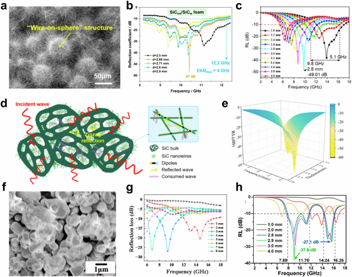
a SEM images of SiCw/SiC porous structure75, b the reflection loss of SiCw/SiC porous structure fabricated75, c the reflection loss of SiCw/SiC porous structure76, d the EMW absorbing mechanism of SiCw/SiC porous structure76, e the reflection loss of rGO/BN/SiC porous structures77, f SEM images of SiC porous structures79, g the reflection loss of SiC porous structures79, h the reflection loss of SiCnw/SiC porous structure82.
Freeze drying is an alternative approach for fabricating porous structures. Zhang et al.77 combined MEX-based 3D printing with freeze drying and thermal treatment to obtain a porous reduced graphene oxide (rGO) skeleton. The BN and SiC coating was introduced by chemical vapor infiltration (CVI) to achieve rGO/BN/SiC porous structures. The rGO/BN/SiC porous structures showed good EMW absorbing properties with an RLmin of −27.1 dB and an EAB of 5.9 GHz, when the thickness was 2.8 mm, as illustrated in Fig. 8e. This performance was attributed to the porous structure, which extends the transmission path of incident microwaves, and the hierarchical structure of the composite material, which enhances multiple scattering of the incident microwaves.
Direct foaming is also an effective technology for fabricating porous structures, allowing for the adjustment of pore size and porosity by controlling the amount and type of foaming agent78. A challenge in integrating direct foaming with 3D printing technology is the creation of a stable, printable foam slurry. Wu et al.79 combined MEX-based 3D printing with direct foaming to fabricate a SiC porous structure, as depicted in Fig. 8f. Dodecyl trimethyl ammonium bromide (DTAB) was used as a foaming agent, added to the SiC slurry, and polyvinyl alcohol was incorporated to maintain the porous structure during printing. After vigorously mixing, a stable foam slurry suitable for MEX-based 3D printing was obtained. The resulting SiC porous structure, sintered at 1650 °C and with a thickness of 3 mm, exhibited excellent EMW absorbing properties, with an RLmin of −27.1 dB and an EAB of 3.4 GHz, as shown in Fig. 8g.
The sacrificial template method is a technique commonly used to prepare materials with a specific porous structure. This method usually involves mixing a sacrificial template (such as polymer foam, metal foam, or natural material) with the desired material precursor, and then removing the template to leave the desired porous structure80,81. Wang et al.82 combined the sacrificial template method with VPP-based 3D printing to fabricate SiCnw/SiC porous structure. SiO2 powder was used as a carbothermal reduction raw material and as an in situ porous agent. PMMA was added to the photocurable slurry to prevent the sample from collapsing after debonding. The as-obtained SiCnw/SiC porous structure could achieve an RLmin of −49.10 dB and an EAB of 3.93 GHz, when the thickness was 2.60 mm, as illustrated in Fig. 8h.
Honeycomb structures
Honeycomb structures, with their unique architecture, have found significant applications in the field of EMWA, offering advantages such as increased specific surface area for enhanced absorption and scattering, broadband absorption capabilities, improved impedance matching, and reduced weight due to their lightweight design83,84.
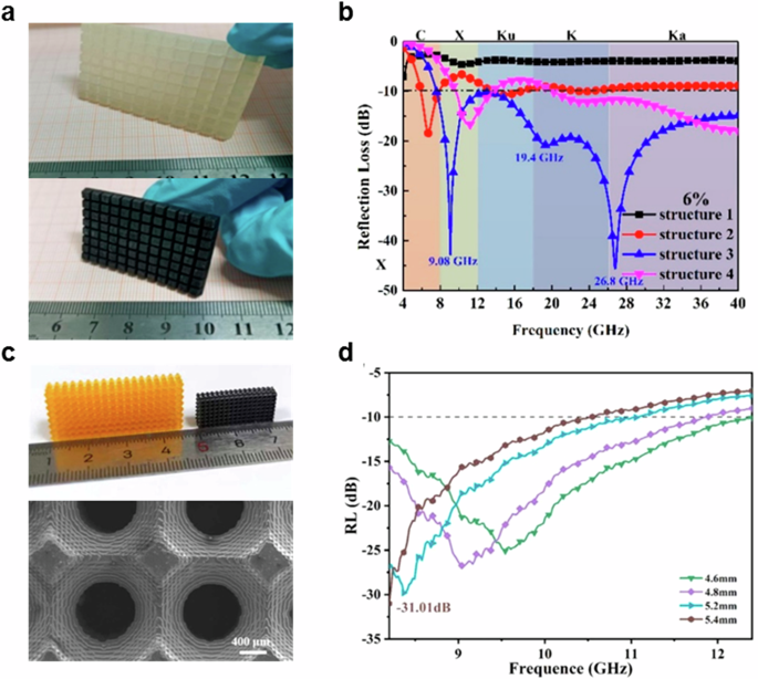
Mei et al.85 demonstrated the tunability of honeycomb structures by controlling the angles, which in turn adjusted the EMW absorbing properties. The Al2O3/SiCw honeycomb structures with different angles were fabricated by VPP-based 3D printing combined with CVI, as shown in Fig. 9a. Notably, the 30° angled Al2O3/SiCw honeycomb structure exhibited better EMW absorbing properties with an RLmin of −63.65 dB and an EAB of 4.2 GHz (from 8.2 to 12.4 GHz), when the thickness was 3.5 mm, as depicted in Fig. 9b. Pan et al.53 utilized VPP-based 3D printing to create SiCN honeycomb structures for EMWA. Compared to the bulk SiCN ceramic, the RLmin of the SiCN honeycomb structure was significantly improved from −23.3 dB to −49.0 dB, as illustrated in Fig. 9c. The SiCN honeycomb structure had a low density of 0.72 g/cm3 and specific compressive strength of 333.3 MPa/(g⋅cm−3), indicating its potential for lightweight, load-bearing, and EMW absorbing ceramic panels, as shown in Fig. 9d. Interestingly, Wang et al.59 employed the large mutation genetic algorithms programmed to optimize the design of SiC honeycomb structures, which were then easily fabricated by MEX-based 3D printing, as depicted in Fig. 9e. They investigated the EMW absorbing properties of the SiC honeycomb structure under various conditions and found that it showed better EMW absorbing performance under oblique incidence, as shown in Fig. 9f. The SiC honeycomb structure exhibited a broadband EMW absorbing properties with an EAB of 34.64 GHz (from 4.85 to 39.49 GHz) when the incident angle was 60o. Even after exposure to high temperatures, the SiC honeycomb structure retained its broadband EMW absorbing properties.
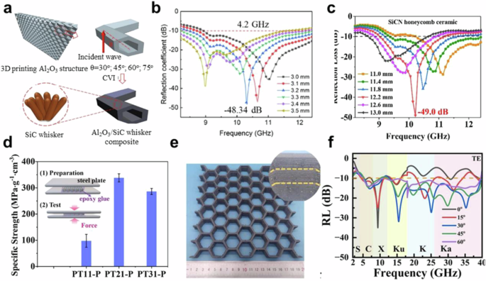
a Schematic diagram of Al2O3/SiCw honeycomb structure fabrication85, b the reflection loss of Al2O3/SiCw honeycomb structure85, c the reflection loss of SiCN honeycomb structure53, d the compressive strength of SiCN honeycomb structure53, e the image of SiC honeycomb structure59, f the reflection loss of SiC honeycomb structure59.
Stepped structures
Stepped structures consist of a series of steps with different heights or widths, forming a stepped geometric shape. The multiple interfaces of the stepped structure can cause EMW to scatter multiple times inside the material, extending the propagation path of EMW and increasing the chance of absorption86.
Liu et al.62 designed and fabricated a MoS2/PyC-Al2O3 stepped structure via VPP-based 3D printing, as shown in Fig. 10a. This study highlighted the significant enhancement in EMW absorbing performance, attributed to the innovative design of both microscale nano/microstructures and macroscale structures within the absorber. The resulting MoS2/PyC-Al2O3 stepped structure, with a thickness of 6.5 mm, achieved an EAB of 35 GHz (from 5 to 40 GHz) and retained a broadband EMW absorbing performance even at elevated temperatures up to 673 K, as illustrated in Fig. 10b. Continuing the exploration of stepped structures, Zhou et al.87 utilized VPP-based 3D printing to fabricate a PyC/Al2O3 stepped structure with microchannels. After investigating the impact of channel dimensions and count on the composite’s permittivity, they optimized the microchannels within the stepped structure to achieve superior EMW absorbing properties, as illustrated in Fig. 10c. The tailored PyC/Al2O3 stepped structure delivered an EAB of 12 GHz from 6 to 18 GHz, as seen in Fig. 10d, offering a novel approach to customizing EMW absorbing properties through the integration of microchannels in 3D-printed structures. Zhou et al.58 further expanded the horizons by employing VPP-based 3D printing combined with the PIP process to create a SiC stepped structure, as shown in Fig. 10e. This structure, optimized using large mutation genetic algorithms, featured a design distinct from conventional stepped structures, incorporating concave and suspending shapes. The resulting SiC stepped structure exhibited a broadband EMW absorption with an EAB of 33.04 GHz from 6.96 to 40 GHz and demonstrated broadband absorption performance under oblique incidence across a wide range of angles both in transverse electric (TE) polarization and transverse magnetic (TM) polarization, as detailed in Fig. 10f.

a The MoS2/PyC-Al2O3 stepped structure62, b the reflection loss of MoS2/PyC-Al2O3 stepped structure at different temperatures62, c the design of microchannels and stepped structures87, d the reflection loss of PyC/Al2O3 stepped structures87, e images of SiC stepped structures58, f the reflection loss of the SiC stepped structure in TE and TM polarization58.
Twisted cross structures
Twisted cross structures are prevalent in the field of EMWA, with their absorbing performance being optimized by adjusting the twist angle, and the distribution of the cross points. Mei et al.88 first fabricated Al2O3 twisted cross/flat structures via VPP-based 3D printing, further enhanced by in situ growth of SiC nanowires to form Al2O3/SiCnw/SiOC twisted cross/flat structures. They refined the microstructure of SiC nanowires by modulating the immersion and cracking time of the precursor solution and the ferrocene catalyst content, thereby improving the EMW absorbing performance. The optimized Al2O3/SiCnw/SiOC twisted cross/flat structure achieved an RLmin of −44.35 dB at a thickness of 2.5 mm and an EAB of 3.6 GHz in the X-band at a thickness of 2.8 mm, as depicted in Fig. 11a. Building on this, they89 incorporated CNTs as a conductive phase to create a conductive network, significantly improving EMW absorbing properties. The resulting Al2O3/CNTs/SiCnw/SiOC twisted cross/flat structure exhibited an RLmin of −56.84 dB at a thickness of 2.8 mm and an EAB of 4.2 GHz at a thickness of 3.2 mm, as shown in Fig. 11b. Zhou et al.50 optimized the parameters of the unit structure and then fabricated SiOC twisted cross structure via VPP 3D printing, as shown in Fig. 11c. This design minimally affected the attenuation of the material while significantly reducing the complex dielectric constant. This SiOC twisted cross structure possessed an RLmin of −56.11 dB at a thickness of 2.7 mm with a corresponding EAB of 3.13 GHz (from 9.27 to 12.4 GHz). An increase in the thickness to 2.9 mm expanded the EAB to 3.76 GHz, as shown in Fig. 11d.
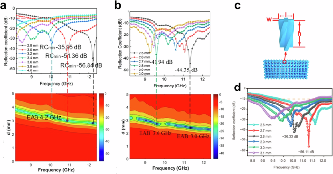
a The reflection loss of Al2O3/SiCnw/SiOC twisted cross/flat structures88, b the reflection loss of Al2O3/CNTs/SiCnw/SiOC twisted cross/flat structures89, c twisted cross-unit and array structures, d the reflection loss of SiOC twisted cross structure50.
Triple periodic minimal surface structures
Triple periodic minimal surface (TPMS) structures are well-known for their complex internal channels and pores, which contribute to the enhanced scattering and reflection of electromagnetic waves inside the structure, thereby increasing the absorption depth and efficiency. Common TPMS structures include the gyroid, diamond, primitive, I-WP, and F-RD, each described by unique parametric equations90. Yao et al.69 utilized VPP-based 3D printing to fabricate SiOC-based gyroid structures with varying shell thickness (ranging from 200 to 400 μm) at a fixed unit cell dimension of 2.54 mm, as shown in Fig. 12a. They introduced a design paradigm that optimizes the EMW absorbing performance by integrating theory, calculation, and experimentation. The SiOC-based gyroid structure with a shell thickness of 300 μm demonstrated superior EMW absorbing properties, with an RLmin of −70.3 dB at a thickness of 2.73 mm and an EAB of 4.2 GHz at a thickness of 3.26 mm, as illustrated in Fig. 12b. Wang et al.91 employed a similar strategy to design and fabricate SiOC gyroid structures by VPP-based 3D printing. They controlled the pre-ceramic composition to tailor the composition and microstructure of SiOC ceramics and then combined it with gyroid structural design to obtain an absorbing structure with good performance, as depicted in Fig. 12c. At a porosity of 51%, the SiOC gyroid structure achieved an RLmin of −31.3 dB at a thickness of 2.6 mm and an EAB of 4.2 GHz (covering the X-band) at a thickness of 3.1 mm, as shown in Fig. 12d. Lu et al.92 also employed the effects of pyrolysis temperature on EMW absorbing properties of SiOC gyroid structures fabricated by VPP-based 3D printing. The SiOC gyroid structure pyrolyzed at 1200 °C exhibited an RLmin of −59.96 dB and an EAB of 4.2 GHz at the thickness of 2.9 mm, as shown in Fig. 12e. They used computer simulation technology (CST) simulation to guide structural design, achieved the integration of simulation, modeling, and experiments, and provided new insights for the development of high-temperature ceramic-based structures for EMWA.
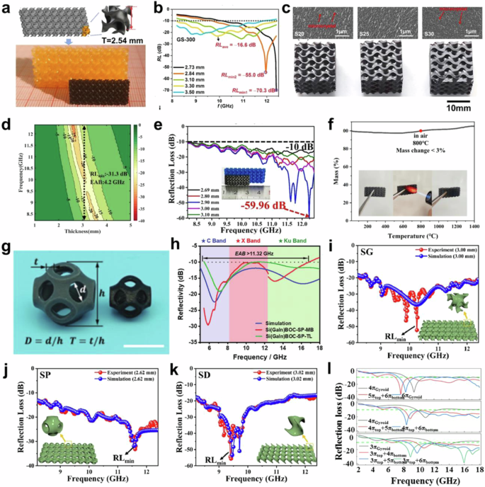
a Images of SiOC-based gyroid structures69, b the reflection loss of SiOC-based gyroid structure69, c Images of SiOC gyroid structures91, d the reflection loss of SiOC gyroid structure91, e the reflection loss of SiOC gyroid structure pyrolyzed at 1200 °C92, f the high temperature oxidation resistance of SiCN gyroid structure93, g images of Si(GaIn)BOC primitive structures70, h the reflection loss of Si(GaIn)BOC primitive structures70, the reflection loss of SiOC TMPS structure with different unit structures: i Schoen G, j Schwarz D and k Schwarz P94, l the reflection loss of SiC/Si3N4 TMPS structure with a double-layer stereo-unit model95.
Furthermore, Tong et al.93 extended the application of TPMS by fabricating SiCN gyroid structures via VPP-based 3D printing. This SiCN gyroid structure could have good oxidation resistance, due to the SiO2 passivation layer formed after oxidation as depicted in Fig. 12f. Additionally, this SiCN gyroid structure possessed an RLmin of −21.12 dB and an EAB of 4.2 GHz at the thickness of 3.22 mm. Xing et al.70 ventured beyond gyroid structures to fabricate Si(GaIn)BOC primitive structures by VPP-based 3D printing. They found the optimal structural parameters through simulation and fabricated a Si(GaIn)BOC primitive structure with a wall thickness of 1 mm, a hole diameter of 1.85 mm, and a unit height of 10 mm, as illustrated in Fig. 12g. The Si(GaIn)BOC primitive structure possessed an EAB of 11.36 GHz (from 5.4 GHz to 18 GHz) and remained the broad EAB even when the incident angle was up to 40°, as shown in Fig. 12h. Lu et al.94 further expanded the exploration by fabricating SiOC TMPS structures with different unit structures (gyroid, diamond, primitive) by VPP-based 3D printing and comparing their EMW absorbing properties. All three structures achieved an EAB of 9.80 GHz (8.2–18.0 GHz), covering the entire X-Ku band. In addition, the diamond structure possessed an RLmin of −55.68 dB at a thickness of 3.02 mm, as shown in Fig. 12i–k. Yu et al.95 also investigated the impacts of unit structure on EMW absorbing properties of structures. They fabricated SiC/Si3N4 TMPS structures with different unit structures by VPP-based 3D printing. They detailed the effects of TPMS stereo-unit size and wall thickness on EMW absorbing properties. Then they designed a double-layer stereo-unit model, which was composed of two gyroid structures with different stereo-unit sizes. This structure showed excellent absorbing properties with an EAB of 11.12 GHz (from 6.88 GHz to 18 GHz), as shown in Fig. 12l.
Other structures
In addition to the aforementioned structures, other researchers have expanded the application of 3D printing technologies to other ceramic-based structures for EMWA.
Pyramid structures, recognized for their effectiveness in EMWA, have garnered significant attention. Liu et al.96 successfully fabricated a carbon nanofiber (CNFs)-SiBCN pyramid structure via VPP-based 3D printing, as illustrated in Fig. 13a. The geometric parameters of height, base width, and spire width are crucial to the pyramid structural design. Through optimization using CST simulation, they enhanced the EAB of the structure. The optimized CNFs-SiBCN pyramid structure could have an RLmin of −46.0 dB with a corresponding EAB of 32.4 GHz, as depicted in Fig. 13b.
a Images of CNFs-SiBCN pyramid structures96, b the reflection loss of CNFs-SiBCN pyramid structures96, c images of SiCN lattice structures97, d the reflection loss of SiCN lattice structures97.
Lattice structures have also garnered interest. Hu et al.97 developed a SiCN lattice structure via VPP-based 3D printing. They designed and optimized the lattice structures composed of hollow spheres, as shown in Fig. 13c. Comparing the lattice structures with different hollow sphere sizes, the SiCN lattice structure showed better EMW absorbing properties with an RLmin of −31.01 dB at a thickness of 5.2 mm and an EAB of 4.2 GHz at a thickness of 4.6 mm, when the hollow sphere size was 2 mm, as shown in Fig. 13d.
As illustrated in Table 2, the integration of advanced 3D printing technologies with ceramic materials and innovative structural designs provides broad prospects for the development of high-performance EMW absorbing materials. By optimizing the material and structure combinations, these advanced materials can achieve efficient absorption with specific frequency ranges. Compared to bulk ceramic materials, the RLmin and EAB of ceramic structures demonstrate significant improvements. Notably, through strategic structural optimization, it is possible to attain both a lower RLmin and a broader EAB, showcasing the potential of these materials in the field of EMWA.
Limitations and development tendency
In the past decades, benefiting from the rapid development of advanced 3D printing technologies, ceramic materials with complex structures can be achieved more easily and efficiently, further expanding the research of ceramic materials in the field of EMWA. The focus of research on ceramic absorbing materials has evolved from single ceramics to a diverse range of ceramic-based composites. An increasing number of researchers are now concentrating on the structure design of these materials to achieve high-performance EMW absorbing capabilities. Despite these significant advancements, there is still considerable work ahead to achieve even higher-performance ceramic materials for EMWA.
Novel structure design
In the realm of ceramic-based structure design, the focus has predominantly been on traditional structures such as stepped, honeycomb, and twisted cross structures. However, with the advent of 3D printing technologies, the design and application of ceramic-based TPMS structures have garnered increased attention. Despite these developments, there is a recognized need for greater innovation in the design of absorbing structures, which may be pivotal for further enhancing the performance of new ceramic-based materials for EMWA.
Biomimicry, inspired by the unique microstructures of natural entities, has opened new avenues for structure design. Bionic structures, featuring unique microstructures assembled from functional subwavelength units in an orderly pattern, enable animals and plants with exceptional macroscopic characteristics. High-magnification microscopy has facilitated a deeper understanding and replication of these bionic structures98,99,100. Drawing inspiration from the noctuid moth’s eyes, known for their efficient anti-reflective surfaces, Huang et al.101 designed and fabricated a hierarchical structure with multiband EMW adaptability, as illustrated in Fig. 14a. This hierarchical structure achieved a broad EAB of 9.84 GHz (from 8.04 GHz to 17.88 GHz), almost covering the whole X and Ku bands, as shown in Fig. 14b. Similarly, Fang et al.102 synthesized a bionic carbon foam structure coated with Fe3C particles, taking cues from octopus tentacles, as shown in Fig. 14c. This bionic C/Fe3C foam structure presented excellent EMW absorbing properties with an RLmin of −53.14 dB at a thickness of 4.35 mm and an EAB of 6.52 GHz at a thickness of 2.40 mm, as shown in Fig. 14d.
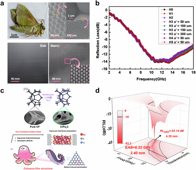
a SEM images of moth eyes, slab, and bionic hierarchical structures101, b the reflection loss of bionic hierarchical structures101, c schematic diagram for bionic octopus-like C/Fe3C foam102, d the reflection loss of C/Fe3C foam102.
To advance the field further, the methodology of design must also evolve. The current iterative process of parameter adjustment is not only time-consuming but also potentially inefficient. Integrating artificial intelligence and machine learning technologies, such as genetic algorithms103 and particle swarm optimization104, could revolutionize the optimization of ceramic-based structure designs. These algorithms predict and optimize the EMWA performance of materials by iteratively improving design variables such as material composition, microstructure, and geometry. These advanced techniques hold the promise of more efficient and accurate predictions and regulation of material absorption performance.
Advanced manufacturing technologies
In the aspect of ceramic fabrication, 3D printing is a highly advantageous method, particularly for creating intricate structures. This technology streamlines the manufacturing process by integrating and automating the design-to-creation process. 3D printing technologies, including VPP, PBF, BJT, and MEX, offer unique advantages for EMWA applications, each suitable for specific scenarios. VPP-based 3D printing excels in high-precision and complex geometric structures, making it ideal for high-frequency EMWA applications that require intricate absorbing structures. PBF-based 3D printing stands out for its ability to process various metal and ceramic materials, enabling the creation of gradient structures for wideband or frequency-selective absorption. BJT-based 3D printing is particularly suitable for applications demanding lightweight and high specific surface area, such as radar absorption in aerospace. MEX-based 3D printing has proven effective in manufacturing continuous fiber-reinforced composite materials, providing high mechanical strength and electromagnetic properties for applications like military vehicle armor. However, the applications of 3D printing in ceramic materials do encounter certain limitations, highlighting these areas that require further exploration and improvement.
The integration of multi-material 3D printing technology with ceramic materials is a significant trend in the development of ceramic materials for EMWA. However, the distinct properties of different ceramics often pose challenges in achieving effective interface bonding during the 3D printing process. To address this, Zhang et al.105 demonstrated an innovative approach by applying gradient ceramic layers to mitigate thermal mismatch stress among multi-ceramic triangle structures via VPP-based 3D printing, as depicted in Fig. 15a. This strategy not only showcases the potential of 3D-printed multi-ceramic structures but also highlights the need for the development of new or the enhancement of existing 3D printing technologies. Moreover, Yu et al.106 directly mixed zirconia and alumina to achieve a zirconia-toughened alumina (ZTA) slurry suitable for MEX-based 3D printing. The resulted ZTA possessed a bending strength of 422.5 MPa and a fracture toughness of 6.2 MPa m1/2. In contrast, it is hard to combine the different materials (such as metal/ceramic composites) by thermally co-processing together because they have significantly different sintering temperatures. The temperature at which a ceramic can effectively melt and flow may be higher than that for metals, and in some cases, it is so high that the metal evaporates before the ceramic has a chance to start flowing. When preparing Ti6Al4V/Al2O3 multi-material structures, Zhang et al.107 observed that Al2O3 powders absorbed sufficient laser energy to melt. However, before the Al2O3 could melt and bond, the Ti6Al4V particles began to evaporate, as shown in Fig. 15b. Lu et al.108 presented a sequential fabrication of Al/Al2O3 composites. They initially produced an Al2O3 scaffold by VPP-based 3D printing, followed by the introduction of Al by melt infiltration. However, the geometrical degree of freedom is limited in sequential fabrication. This highlights the complexity of processing multi-material structures and the importance of developing printing parameters that can accommodate the thermal properties of different materials within the same build, ensuring that each material can be effectively processed without compromising the integrity of the final structure.
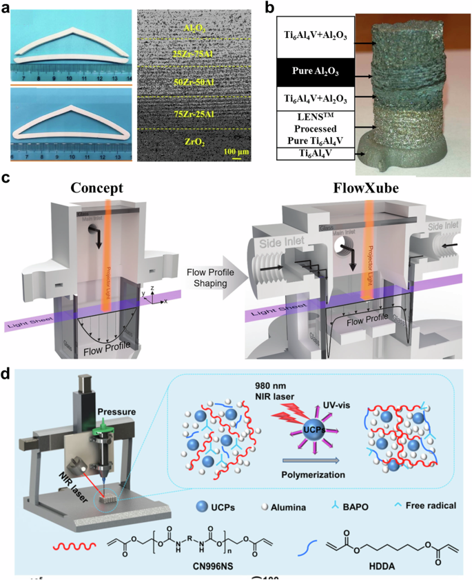
a Multi-ceramic triangle structures using VPP 3D printing105, b Ti6Al4V/Al2O3 multi-material structures, c schematic diagram for volumetric 3D printing109, d schematic representation of NIR-assisted MEX-based 3D printing110.
The pressing issue of reconciling size and resolution in 3D printing demands novel solutions. VPP-based 3D printing is adept at fabricating intricate structures with high precision but is limited in the scale of the structures it can produce. MEX-based 3D printing, in contrast, enables the creation of large-scale structures yet sacrifices precision. Volumetric 3D printing, as advanced by Stüwe et al.109, demonstrated the potential to resolve not only the trade-off between high production rates and high resolution but also the long-standing issue of reconciling size and precision. By enabling the continuous printing of objects with smooth surfaces and accurate dimensions (as shown in Fig. 15c), this technology paved the way for overcoming the limitations that traditionally restricted the size of printable parts while maintaining high-resolution details. Moreover, researchers like Zhao et al.110 have developed a ceramic printing method that leveraged MEX-based 3D printing and near-infrared (NIR) induced photopolymerization, as depicted in Fig. 15d. This method achieved unsupported multi-scale, large-span ceramic printing, with the ability to in situ cure multi-scale filaments ranging from 410 µm to 3.50 mm in diameter, significantly improving the resolution of MEX-based 3D printing.
Real experimental testing
Based on the current state of experimental testing in the field of ceramic-based materials for EMWA, a prevalent limitation is that the majority of researchers have concentrated their evaluations within the 2–18 GHz frequency range, neglecting to examine the absorption performance of materials under diverse environmental conditions. The lack of testing across varying temperatures, incident angles, and polarization modes is a significant oversight, as it impedes a comprehensive assessment of the stability and adaptability of ceramic-based materials in real-world EMWA applications.
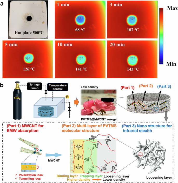
Currently, the evaluation of EMW absorbing properties for ceramic materials is predominantly measured at room temperature, with little exploration into high-temperature performance. Existing high-temperature EMWA testing relies on muffle furnace heating, which is limited to temperatures not exceeding 1000oC. This limitation hinders the verification of the potential of ceramic materials for high-temperature applications. Therefore, there is an urgent need to develop advanced testing equipment capable of assessing the EMW absorbing performance of ceramics at elevated temperatures, which would facilitate a comprehensive understanding of their suitability for high-temperature EMWA. Furthermore, as the development of multifunctional ceramic materials progresses, there is an emerging trend toward more comprehensive testing. This includes the assessment of mechanical properties, thermal characteristics, and EMW absorbing capabilities, ensuring a holistic evaluation that reflects the multifaceted nature of these advanced materials. Jiang et al.54 synthesized SiC nanowires in situ in SiBCN ceramic aerogels through catalyst-assisted annealing technology, and successfully prepared polymer-derived SiBCN/SiCnw composite aerogels. This composite aerogel had lightweight and excellent heat insulation performance, as shown in Fig. 16a, making it an ideal choice for electromagnetic wave absorption materials. These materials are particularly favored in aircraft and military applications because they cannot only withstand aerodynamic heating but also provide electromagnetic wave stealth capabilities. For infrared (IR) stealth and EMWA double stealth device, Ma et al.111 fabricated a novel pre-polymerized vinyl trimethoxy silane (PVTMS)@MWCNT nano-aerogel, as illustrated in Fig. 16b. This aerogel showed superior EMWA property (cover all Ku-band) and thermal IR stealth property (ΔT reached 60.7oC).
a Infrared images of SiBCN/SiCnw aerogel54, b schematic representation of PVTMS@MWCNT nano-aerogel111.
For a comprehensive understanding of the sustainability of 3D-printed ceramic-based materials for EMWA, all required inputs and outputs need to be considered across the different life cycle stages of 3D-printed products. Kokare et al.112 illustrated the life cycles of a 3D-printed product. Many researchers have paid attention to environmental sustainability, and a framework for conducting environmental life cycle assessment is defined by the ISO 14044:2006 standard. However, the economic and social dimensions of life cycle assessment are neglected. Moreover, the focus on the life cycle stages after 3D-printed ceramic-based materials for EMWA is necessary, considering the extreme service environments they may encounter.
Summaries
This review provides an in-depth analysis of the integration of 3D printing technologies with ceramic materials and structures for EMWA. It emphasizes the transition from material-centric to structure-centric design, which has significantly advanced the performance of EMW absorbing materials. Despite substantial progress, challenges remain, including narrow absorption bandwidths and precision limitations in multi-material printing. Furthermore, current experimental testing is often limited to room temperature and specific frequencies, which restricts a full assessment of material capabilities. Fortunately, the synergy of 3D printing and ceramics presents promising opportunities for developing advanced EMW absorbing materials. Future development in this field will focus on innovative structural designs, enhanced manufacturing technologies, and a more comprehensive approach to experimental testing that considers the multifunctional aspects of these materials.


Responses