Stretchable optoelectronic synapses with ultraviolet to near-infrared perception for retina-inspired computing and vision-adaptive sensing
Introduction
Synaptic transistors (STs) that can memorize and process signals in a single device have drawn extensive attention for potential applications in next-generation artificial intelligence (AI) based on brain-inspired neuromorphic computation. The high-efficient in-memory computing (IMC) and learning abilities make the ST be one of the hotspots of current research. As a special kind of STs, the optoelectronic synapse transistors (OST) that can perceive, process and memorize both electrical and optical signals is particularly attractive1,2,3, because it has additional abilities of visual perception and/or visual self-adaptation/regulation similar to the human retina. However, the reported OSTs generally exhibit monotonous functionality and poor biocompatibility (unstretchable/undeformable), which cannot perform complex tasks in dynamic/unstructured environments such as in wearable and implantable electronics4,5. Therefore, stretchable/deformable OSTs are extremely desirable for the vision-inspired neuromorphic systems with free deformation and cross-scale modulus adaptability6,7. Compared to the structurally stretchable design, the intrinsically stretchable design enables more convenient fabrication, higher versatility and availability, becoming an inevitable componence for next-generation human-oriented applications8. Notably, intrinsically stretchable synaptic devices based on organic semiconductors are particularly appropriate for the purpose of emulating the functions of living systems owing to their mechanical compliance, biocompatibility and excellent optoelectronic properties1,3,8,9,10,11,12,13,14,15,16,17,18,19. However, relatively fewer works have been carried out on stretchable organic optoelectronic synaptic transistor (s-OOSTs) based on inherently stretchable materials featuring both highly reliable electrical synaptic plasticity and multi-wavelength (broadband) vision-inspired neuromorphic response. Most of stretchable photosensitive organic semiconductors typically have a narrow absorption range or limited mechanical ductility. Tae-Woo Lee et al. constructed a stretchable organic nanowire synaptic transistor (s-ONWST) with a semiconductor of FT4-DPP-based polymer, but external photoreceptors are required to convert the external optical signals to electrical signals, which increases the complexity and reduces the efficiency17.
In this paper, a broadband (365–1050 nm) responsive s-OOST based on intrinsically stretchable, high-mobility, narrow-bandgap, high-relaxation-time organic semiconductor was constructed to achieve brain-inspired memory/computation and retina-inspired visual perception/adaptation. The s-OOSTs exhibited high transconductance (86 mS, highest in synapses) at a low voltage (−1 V) and could stand against 50% multidirectional strain. When stimulated by the gate pulse, the postsynaptic current (PSC) of the s-OOSTs exhibited neuromorphic behaviors, such as conversion from short-term plasticity (STP) to long-term plasticity (LTP), spike duration-dependent plasticity (SDDP), pair pulse facilitation (PPF, as high as 264%), spike number-dependent plasticity (SNDP) as well as “learning-forgetting-relearning” behaviors (with a high recognition accuracy of 88.75% simulated by handwritten digital datasets). Furthermore, the s-OOSTs can be stimulated by the light from ultraviolet (UV) to near-infrared (NIR) (365 nm–1050 nm), which is the widest wavelength response ever report. The relaxation time of the s-OOSTs changes greatly with the wavelengths of the incident light, making the devices possess additional abilities of light plasticity, color identification and visual self-adaptation similar to human retina. Moreover, the synaptic performance was investigated at low temperature and vacuum condition. The broadband spectrum response makes it successfully image the letters “SU” in NIR environment with high contrast ratio in a single-pixel scanning imaging system, which verifies the feasibility for near-infrared imaging and visual response of the single s-OOST devices. Finally, multi-wavelength (365nm-1050 nm) optical synaptic plasticity was investigated for the imaging memory, polychromatic optical communication and information security. A series of “bus” images and letters (coded by wavelength) with different colors were identified and memorized by the s-OOSTs. This research promotes the development of the intrinsically stretchable optoelectronic transistors with broadband response from UV nm to NIR.
Results
Device design philosophy and electrical characteristics
Figure 1a–c show fabrication scheme and electrical properties of the s-OOSTs. The detailed fabrication process is described in Methods section. Step I. and II. in Fig. 1a show the fabrication process of the dextran/TPU films, the schematic structure of the s-OOST and the molecular formulas of the organic semiconductor and the ionic gel. Dextran is a hydrophilic material suitable for peeling off the hydrophobic thermoplastic polyurethane (TPU) film from the wafers20. TPU is a transparent, elastic polyurethane material with excellent film forming ability and high stretchability, which meets the demand of smooth and dense substrate for the organic semiconducting films21,22. The organic semiconductor—Poly-diketo-pyrrolopyrrole-selenophene-x hybrid siloxane-based side chains (PTDPPSe-xSi, x = 3–7)) —is an intrinsically stretchable a donor-acceptor (D-A) material23. Specifically, the PTDPPSe main chain has narrow bandgap and excellent charge transport properties. A certain length of the hybrid siloxane-based side chains (x = 6 in this paper, that is, PTDPPSe-6Si) was grafted onto the polymer main chain to enhance its stretchability. The PTDPPSe-6Si has the advantages of high mobility (>1 cm2/Vs), high stretchability (≥100%), narrow gap (1.50 eV), long relaxation time and high photoelectric conversion efficiency, which is extremely attractive in the field of optoelectronic synaptic devices.
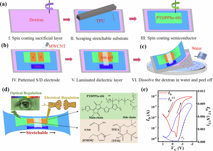
a Preparation of dextran/TPU/PTDPPSe-6Si. b Preparation of stretchable SWCNT source/drain (S/D) and gate electrodes/stretchable ion gels. c Removing the water-soluble sacrifice layer to get an intelligent sensing/optoelectronic integrated organic stretchable synapse. d Schematic structure of the s-OOSTs and the molecular formulas of the organic semiconductor and ionic gel. e Transfer curves of the s-OOSTs.
The multi-wall carbon nanotubes (MWCNTs) electrodes were deposited by spraying process (Fig. 1b)24. Then, an ionic gel film was laminated onto the channel25. After that, the device was immersed in deionized water to remove the dextran sacrificial layer so as to peel off the s-OOST from the substrate (Fig. 1c). Supplementary Fig. 1a–c show the scanning electron microscope (SEM) images of the TPU, PTDPPSe-6Si and MWCNT, respectively. The surface of the TPU substrate was smooth, and the PTDPPSe-6Si film covered well onto the TPU substrate without any cracks. The MWCNTs were seen clearly in the inset of Supplementary Fig. 1c. Figure 1d shows the schematic structure of the s-OOST and the molecular formulas of the organic semiconductor and the ionic gel. Figure 1e shows the transfer curves of the s-OOSTs. The drain current (ID) was obtained by sweeping the gate voltage (VG) from 1 to –2 V and then back to 1 V while the drain voltage (VD) was kept at –1 V. The s-OOSTs exhibited large hysteresis that is essential for mimicking the biological synapses that have plasticity ability. The on/off current ratio (Ion/Ioff, switching ability) was ~104, and the threshold voltage (VT) obtained by ID1/2 ~ VG curve fitting was −0.64 V, which means that the s-OOST is enhancement-mode transistors18. Owing to the high mobility of the PTDPPSe-6Si organic semiconductor, a transconductance of as high as 86 mS were attained for the s-OOST (Supplementary Fig. 1d), which is comparable to those of the best organic synaptic transistors ever reported (Supplementary Table 1)12,17,26,27,28,29,30,31,32,33,34,35,36. Supplementary Fig. 2 shows the transfer curves of the s-OOST under repeated forward/reverse sweeps. The device exhibited relatively good repeatability.
Intrinsic stretchability
Figure 2a shows the transfer curves of the s-OOSTs under different levels of mechanical strain along (parallel) to the channel (carrier transport) directions. The ID (at VG = –2 V) of the unstretched s-OOST was ~80 μA. After parallelly stretched for 12.5%, 25% and 50%, the ID decreased to 59, 53 and 34 μA, respectively. The on/off current ratios (Ion/Ioff) and the gm/VT of the s-OOSTs under different parallel strains are plotted in Fig. 2b, c, respectively. When the s-OOSTs were vertically stretched for 12.5%, 25% and 50%, the ID decreased to 69, 57, and 41 μA, respectively (decreased more slowly compared to the parallelly stretched one). Figure 2d shows the transfer curves of the s-OOSTs under different levels of mechanical strain perpendicular (vertical) to the channel directions. The Ion/Ioff and the gm/VT of the s-OOSTs under different vertical strains are plotted in Figs. 2e and 2f, respectively. The decrease in Ion and gm under vertical strains was less than those under parallel strains, because the vertical stretching increases the channel width (W), while does not change length (L), resulting in an increase in W/L and a smaller attenuation in Ion and gm. Supplementary Fig. 3 shows the leakage current of the static strain, the leakage current were about 0.41 μA (0%), 0.38 μA (12.5%), 0.20 μA (25%) and 0.4 μA (50%) under parallelly stretching, and 0.41 μA (0%), 0.44 μA (12.5%), 0.41 μA (25%) and 0.36 μA (50%) under vertically stretching. It shows that the EMIM-TFSI ion-gel dielectric layer is able to withstand 50% stain without significant changes in the leakage current. Supplementary Fig. 4a shows the tensile durability of the s-OOSTs under 500 repeated stretch/release cycles (50% parallel strain). After 500 stretch/release cycles, the Ion decreased from ~80 μA to ~50 μA) while the Ioff did not changed much (around 15–20 nA under different strain cycles), resulting a slight decrease in the on/off ratio (Supplementary Fig. 4b). The leakage of the dynamic strain is shown in Supplementary Fig. 4c. It reveals that the s-OOSTs are able to withstand 500 stretch/release cycles. The comparison of the static and dynamic strain of the s-OOSTs with the devices reported before is summarized in Supplementary Table 2.
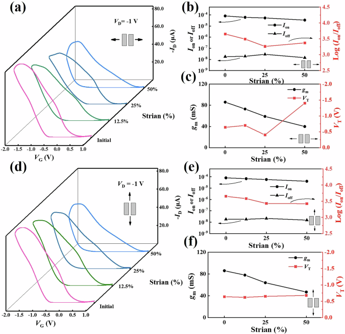
a Transfer curves of the s-OOSTs under parallel strains. b Ion, Ioff and Log (Ion/Ioff) of the s-OOSTs under parallel strains. c gm and VT of the s-OOSTs under parallel strains. d Transfer curves of the s-OOSTs under vertical stains. e Ion, Ioff and Log (Ion/Ioff) of the s-OOSTs under vertical strains. f gm and VT of the s-OOSTs under parallel strains.
Synaptic behaviour regulated by electrical pulses
Supplementary Fig. 5a shows the schematic transmission principle of the neural system. A biological synapse is a structure that transmits neural information from one neuron to the next in the form of serial propagating action potentials. This process can be simulated by the s-OOSTs. Supplementary Fig. 5b shows the working principle of the s-OOSTs that emulates biological synaptic functions. When a pulse signal is applied to the gate, the channel current between source and drain changes, corresponding to ΔPSC (the changes of the postsynaptic current), which can be modulated by a series of factors such as pulse width. The ΔPSC reflects the variations in synaptic weights that represent connection strength between two synaptic neurons and associate with the learning and memory processes in human brains. The synaptic plasticity can be mainly separated into STP and LTP according to the duration to assess memory characteristics.
To characterize the SDDP of the s-OOSTs, presynaptic pulse signals with different pulse widths ranging from 50 to 1000 ms were applied to the gate. Supplementary Fig. 5c depicts the ΔPSC after applying pulse signals to the gate of the s-OOSTs. The ΔPSC increased from 14 to 108 μA when the pulse width increased from 50 to 1000 ms. When stretched by 50%, the s-OOSTs maintained good SDDP with ΔPSC increased from 3 (50 ms) to 32 μA (1000 ms). The SDDP behavior is due to the increase in the number of ions accumulated at the ion gel/channel interface with an increasing pulse width (the ions have more time to move to the interface). The response current (ReC) and the memory current (MeC) are defined as Eqs. (1) and (2), respectively1.
Where I0 represents the initial ΔPSC before triggering; I1 indicates the peak ΔPSC during triggering; and I2 indicates ΔPSC for 1 s after triggering. The s-OOSTs showed increasing memory level (the MeC increased from 7 to 63 μA) with an increasing pulse width (from 50 to 1000 ms). The plasticity transferred from STP to LTP (if defining MeC > 15 μA for LTP) when the pulse width reached 200 ms.
PPF is a typical form of STP, which is defined as the ratio of the height of the second peak ΔPSC (A2) to the height of the first peak ΔPSC (A1) under the stimulation of two consecutive VG pulses with the same shape. The PPF index is defined as18
The PPF index is greater than 100%, because some of the induced ions in the first pulse still exist at the ion gel/channel interface, resulting in a higher conductance in the second pulse. Supplementary Fig. 5d shows the ΔPSCs of the s-OOST triggered by two successive presynaptic pulses with a Δt of 1000 ms. A PPF index of 185% was obtained for the unstretched s-OOSTs under electrical pulse simulation. After stretched by 50%, the PPF index was 167%. The PPF index can be strengthened by adjusting the interval between the two successive pulses. Supplementary Fig. 6 shows the ΔPSCs of the s-OOSTs triggered by two successive presynaptic pulses with different Δt. The lower PPF for longer Δt is due to the relaxation of the ions. Upon stretching by 50%, the PPF index did not changed much. Energy efficiency is necessary for neuromorphic computation. When stimulated by a single VG pulse (–30 mV, 10 ms), the PSC signal (with an amplitude of 3.7 pA) remained clearly detectable even at a VD of −100 μV. According to Eq. (4)10
the minimum energy consumption of the single-event operation of the s-OOSTs was 3.7 aJ (Supplementary Fig. 7). The signal to noise ratio (S/N) is also shown in Supplementary Fig. 7. The SNR of the PSC signal is determined by the Eq. (5)37
The S/N was calculated to be 18.5, 33.5 and 68, corresponding to the pulse width of 10 ms, 20 ms and 50 ms, respectively. For neuromorphic engineering applications, both high SNR and low energy consumption are needed. The corresponding SNR was calculated by Eq. (5) to be 12.68 dB, 15.25 dB and 18.30 dB, and the corresponding energy consumption was 3.7 aJ, 13.4 aJ and 224 aJ, respectively. The summarized S/N and SNR value are shown in Supplementary Table 337,38,39,40,41,42. The S/N and SNR value were relatively high even at VD = − 100 μV in a relative energy-efficient state.
The response and memory level of the s-OOSTs also increased with an increasing pulse number (N). Supplementary Fig. 8 shows the ΔPSCs of the s-OOSTs when applying pulse signals with different pulse number of 5–50 to the gate of the s-OOSTs. ΔPSCs increased as the pulse number increased. As the pulse number increased from 5 to 50, the ReC increased from 83 to 227 μA (Supplementary Fig. 9a), and MeC strengthened from 31 μA to 147 μA (Supplementary Fig. 9b). Similar results were found under 50% strain.
Brain-inspired computation
“Learning-forgetting-relearning” behavior is a critical indicator for the learning and memory ability of human brains. As shown in Fig. 3a, after a period of learning by applying 50 successive VG pulses, the ΔPSC increased to a peak value and then decreased slowly, which is similar to repetitive learning behavior of human brain. After 60 s forgetting, the ΔPSC was still much larger than the initial ΔPSC. It reflects that the s-OOSTs has excellent memory ability. After the second learning period with much fewer pulses (20 successive pulses), the s-OOSTs reached a higher ΔPSC than that after the first period of learning strength, indicating that the s-OOSTs have certain associating and relearning ability. Moreover, after the second learning period, the forgetting time increased to >>60 s. This indicates that the s-OOSTs can reduce the learning time and increase the memory time through training. Similar results can be found under 50% strain (Fig. 3b). The result shows that the s-OOSTs have great potential for deep learning ability.
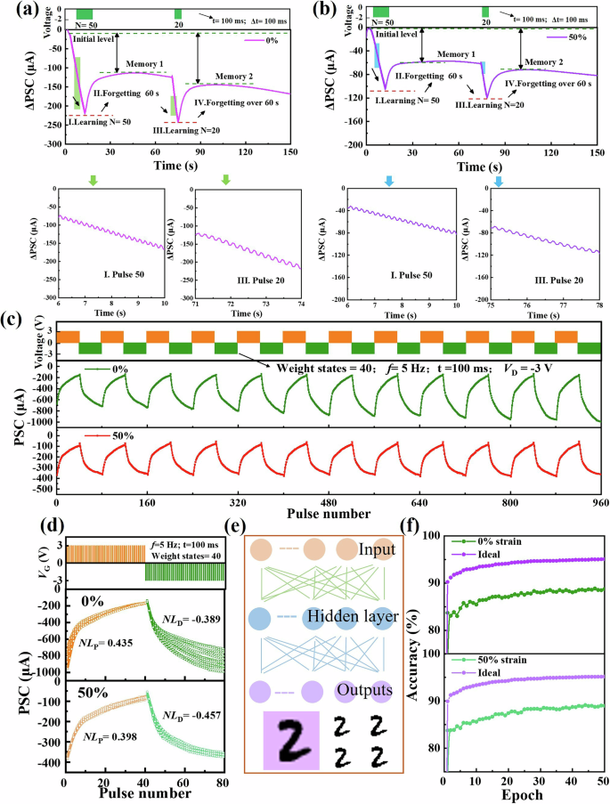
a Learning-forgetting-relearning” brain-inspired behaviors under 0% strain. b “Learning-forgetting-relearning” brain-inspired behaviors under 50% strain. c ΔPSC under successive positive-negative pulse groups. d Average NL value at different strains. e MNIST dataset and neural network with three layers of ANN. f The recognition accuracy of 28 × 28 pixel handwritten digital images with training epochs measured at 0% and 50% strains.
Figure 3c shows the potentiation and depression (PD) response of the s-OOSTs under 12 PD cycles (each cycle included 40 pulses of +3 V and 40 pulses of −3 V in series, the frequency was 5 Hz, Δt = 100 ms). In each cycle, the PSC changed from about −800 μA to about −169 μA after 40 potentiation pulses and then changed to about −890 μA after 40 depression pulses, reflecting good cycling stability with multiple PD pulse sets. To investigate the PD linearity of the s-OOSTs, the nonlinearity (NL) is introduced, which can be expressed as Eq. (6) 43.
Where IP and ID are actual potentiation and depression of the synaptic current, respectively; and ILinear is the ideal linear current. Lower NL represents better linearity. As depicted in Fig. 3d, The NLP was 0.435 and and the NLD was −0.389 for the unstretched s-OOSTs. Upon stretching by 50%, the NLP and NLD were calculated to be 0.398 and −0.457, respectively. The result reflects that the s-OOSTs have good linearity, uniformity, and repeatability even under 50% strain.
The s-OOSTs were used for image recognition by using MNIST dataset to simulate a neural network in recognition tasks. Figure 3e shows the schematic diagram of a representative MNIST hand written digit “2” and a neural network composed of s-OOSTs. The fully connected layers include 784 input neurons, 200 hidden neurons, and 10 output neurons, and the backpropagation algorithm was used for training. The s-OOST was a unit of the array of the synaptic weight layers whose channel conduction changes were considered as weight updates for executing backpropagation algorithms. The cumulative distribution function (CDF) of each conductivity state was recorded to illustrate the device noise, nonlinearity, and asymmetry in the algorithm. CDF is expressed as44:
where ρG (ΔG) is the probability distribution under a certain conductance state as shown in Supplementary Fig. 10. A large image of handwritten digits (28 × 28 pixels) from the MNIST dataset was utilized for the simulation. After 40 training cycles, as shown in Fig. 3f, the recognition accuracy reached 88.7% (0% strain) and 88.9% (50% strain), indicating that the s-OOSTs have potential in applications in brain-inspired computing.
Visual synaptic behaviours regulated by UV-visible-NIR light
Traditionally, artificial vision system consists of optical sensors, data memories and signal processing modules for image recognizing and processing1,18. In the system, the optical sensors sense the external optical signals and convert them to electrical signals before delivery to the memories for storage, and then the signals are processed by the signal processing modules to complete the image processing and classification tasks, causing high latency for data transmission and high power consumption for the overall system. In contrast, in human visual system (Fig. 4a), retinal neurons not only detect light signal but also preprocess visual signals, so the subsequent recognition and decision-making tasks can be done more efficiently and accurately45,46. Here, the s-OOSTs may have the ability of processing light signals efficiently as the human visual system because of the broadband light sensitivity and long relaxation time of the PTDPPSe-6Si semiconductor. The working mechanism of the s-OOST brain-inspired vision system is illustrated in Fig. 4b. The UV-vis-NIR absorption spectra of the PTDPPSe-6Si semiconductor is shown in Supplementary Fig. 11a. The absorption spectra of the PTDPPSe-6Si semiconductor exhibited two typical absorption bands, one for intramolecular charge transfer (ICT, 600 − 1000 nm) between the donor (D) and aceptor (A) conponents, and the other for π − π* transitions (300 − 600 nm), and the two absorption bands “0-0” and “0-1” in Supplementary Fig. 11a were corresponding to the absorption of the aggregated and nonaggregated state. The absorption spectrum can be expressed as
where a (ℏw) is the absorption coefficient; ℏwi is the interval between vibrator levels; vi is the number of phonons in the excited state. The zero order expression of Eq. (6) can be derived as:
a0 (ℏw) represents the fitting results of the absorption of spectrum curve; γ is the width residual disorder; and Δ0 is recombination energy (the band gap EG = 2Δ0). The detailed description and derivation process of the zero order absorption equation are disscussed in Supplementary Note 1 and Supplementary Note 1 Fig. 1 of the Supplementary Information. The fitting parameters of the curve: Δ0 = 0.71 eV (indicating that the PTDPPSe-6Si has excellent emission properties), and γ = 0.08 (indicating that the Gaussian distribution width is narrow and the excitation probability varies greatly at different wavelengths, see Supplementary Fig. 11b). Supplementary Fig. 11c shows the photoluminescence spectrum (PL) excited by an 808 nm light source. Dual emission peaks at 948 nm (1.31 eV) and 1040 nm (1.19 eV) were observed, which present wide and high emission bands “0—0” and “0—1”. Due to the excellent optoelectronic conversion effect of PTDPPSe-6Si with a narrow band gap (EG = 1.50 eV, near the fitting result, EG = 2Δ0 = 1.42 eV), the s-OOSTs were able to generate corresponding PSC by absorbing light with wavelength ranging from UV to NIR light. Supplementary Fig. 12 shows the NIR/fluorescence lifetime of the charge carriers the PTDPPSe-6Si semiconductor excited by different light wavelengths (ex808 nm and 375nm-EPL). The result can be fit by Eq. (10) 1
where τ1, τ2 and τ3 are lifetime parameters, respectively; A1, A2 and A3 are proportional constants. The fitting results are listed in Supplementary Table 4. It is interesting that the lifetimes excited by 808 nm (μs level) is almost 3 orders longer than the lifetimes excited by 375 nm (ns level).
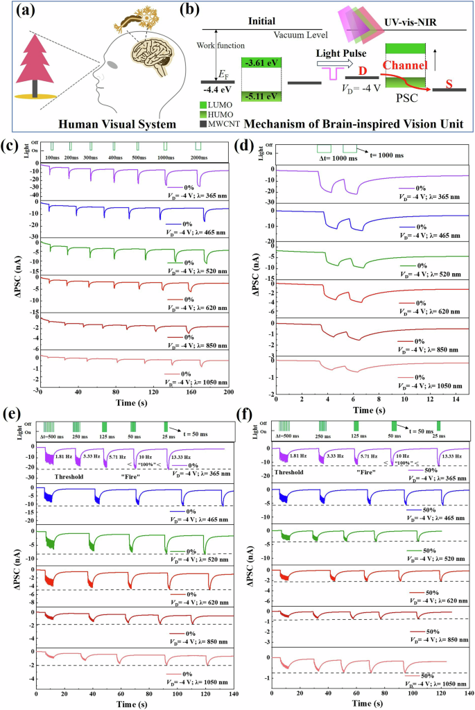
a Schematic structure of human visual system. b Schematic diagram of the s-OOSTs triggered by different light from UV to NIR. c Synaptic plasticity of s-OOST stimulated by single pulse with different pulse widths d Synaptic plasticity of s-OOST stimulated by two successive pulses with Δt = 1000 ms. e The filter effect at 0% strain. f The filter effect at 50% strain.
To investigate the light plasticity of the s-OOSTs, differnt light pulses with wavelengths ranging from UV (365 nm) to visible (blue: 465 nm, green: 520 nm, and red: 620 nm) to NIR (850/1050 nm) were used for regulating the PSC, which is the widest range of light response ever reported in the field of synapses. To investigated the influence of the light intensity on the synaptic behavior, white light with different intensity of 25, 50, 100 μW/cm2 were used to stimulate the s-OOSTs. The ΔPSC increased with the increasing light intensity (Supplementary Fig. 13). The intensity of all kinds of light in the following test was fixed at 25 μW/cm2. As shown in Supplementary Fig. 14, the energy consumption of different light wavelength ranges from 0.2 aJ (λ = 1050 nm) to 1.05 aJ (λ = 365 nm), which is lower than any other stretchable synaptic transistors reported before to the best of our knowledge (see Supplementary Table 2). In addition, the S/N and SNR value of them were obvious when stimulated by VD = − 100 μV with an ultra-low energy consumption, which are also included in Supplementary Table 3. The synaptic behaviors of the s-OOSTs under light pulse stimulation are shown in Fig. 4c–f. The ΔPSC increased as the light pulse width enlarged from 100 ms to 2000 ms, indicating that more pulse duration time of light can induce more carriers in the PTDPPSe-6Si channel. Meanwhile, the ΔPSC also increased with a decreasing wavelength of light, which is ascribed to the higher photon energy for the light with shorter wavelength47. Similar results were found for the s-OOSTs under 50% strain (Supplementary Fig. 15). The corresponding ReC and MeC for the s-OOSTs under light pulse stimulation are shown in Supplementary Fig. 16. Both ReC and MeC were regulated well by the pulse width and wavelength of the incident light even under 50% strain.
The relaxation time (defined by the time for the ΔPSC decreasing from peak to half after removing the light) also increased with an increasing pulse width of the incident light. For example, when the light pulse width increased from 100 ms to 2000 ms, the relaxation time increased from 1.37 s to 1.69 s (under the 1050 nm light). However, unlike ΔPSC, the relaxation time increased with an increasing wavelength of the incident light (Supplementary Fig. 17). For example, when the light wavelength increased from 365 nm to 1050 nm, the relaxation time increased greatly from 0.39 s to 1.69 s. This may be attributed to the long lifetime for the intramolecular charge transfer between donor and acceptor of the PTDPPSe-6Si under red/NIR light stimulation (compared to shorter reconbination time of π − π* transitions stimulated by UV light). According to the test of NIR/fluorescence lifetime in Supplementary Fig. 12, the longer lifetime of NIR light (excited by 808 nm) may lead to a longer memory effect (compared to the ns level lifetime of fluorescence (excited by 375 nm)). On the other hand, the excellent emission properties (according to the permanent Δ0,) and the different wavelength emission possibility (according to the permanent γ) fit by Eq. (9) lead to different resolution and recombination efficiency of excitons, and further result in different ΔPSC trendency. The results indicate that the light wavelength has a much greater impact on the relaxation time than the light pulse width. Figure 4d shows the ΔPSCs of the s-OOST stimulated by two successive light pulses with different wavelengths. And Supplementary Fig. 18 shows the ΔPSCs of the s-OOSTs stimulated by two successive light pulses with different Δt (50–1000 ms), different wavelengths (365–1050 nm) and different strain states (0% and 50%). The corresponding PPF index under light stimulation are shown in Supplementary Fig. 19. The 850 nm NIR light stimulated devices had the highest PPF index (264%), while the 365 nm UV light stimulated devices had the lowest PPF index (137%). The higher PPF under 850 nm NIR light stimulation compared to those under other light stimulation is attributed to the strong absorption and long relaxation time in the 800–930 nm regime, which is originated from D-A intramolecular charge transfer the PTDPPSe-6Si. Upon stretching by 50%, the PPF index did not changed much. The results indicate that the s-OOSTs possesses highly reliable retina-inspired visual plasticity even under 50% strain.
In biological synapses or visual nerves, when the frequency of the presynaptic pulses changes, a synaptic weight change can be generated (SFDP). As the frequency increases, the ΔPSC increases. If the ΔPSC is larger than the threshold, the synapses or visual nerves will “fire” an action potential, which indicates high-pass filtering behavior (filtering characteristics). Here, 10 successive light pulses with a width of 50 ms and different frequencies (1.81, 3.33, 5.71, 10 and 13.33 Hz, corresponding to Δt of 500, 250, 125, 50, 25 ms, respectively) were applied to the s-OOSTs to illustrate the high-pass filtering characteristics, as shown in Fig. 4e, f. The ΔPSCs increased clearly with an increasing frequency. If defining the ΔPSC at a frequency of 10 Hz as the threshold, the unstretched s-OOSTs “fired” an action potential when frequency was higher than 10 Hz. The ratios of the ΔPSCs at different frequency to that at 10 Hz are shown in Supplementary Fig. 20. When the s-OOSTs were stretched at 50%, the ΔPSCs also increased clearly with an increasing frequency, but the ΔPSCs were lower than those of unstretched s-OOSTs. This is mainly because the output current decreases as the applied strain increases. To investigate the heating effect of the s-OOSTs during the light stimulation, the infrared thermometer was used to take pictures after illuminating the device in the UV (λ = 365 nm) and NIR light (λ = 1050 nm) for 10 min (Supplementary Fig. 21). The heating effect is neglectable which may be due to the relatively low intensity of light. Supplementary Table 2 summarized the properties of the multi-wavelength responsive synapses reported before. To the best of our knowledge, our s-OOST has the widest wavelength response among all kinds of ever reported synaptic devices including the rigid1,48,49,50,51,52,53,54,55,56,57,58,59,60,61 /bendable3,6,7,9,10 /stretchable8,15,17,18,62 ones, which indicates that the s-OOSTs have great potential to simulate the animal retinas that can sense the light from UV to NIR.
Synaptic performance at low temperature
The s-OOSTs were further characterized at low temperature (from 293 K to 213 K with the step of –20 K, Supplementary Fig. 22). Under the same temperature condition, the ΔPSC (or ReC) decreased as the light wavelength increased. The ReC level in vacuum condition was quite lower than that in air condition, which might be attributed to the water (or oxygen) doping into the PTDPPSe-6Si channel. More interestingly, the ΔPSC (or ReC) response tendency in vacuum condition was also different from that in air environment. Under vacuum condition, when exposed to the light, the s-OOSTs exhibited a persistent ReC decay (ReCD) over time (Supplementary Fig. 23), which might be attributed to the faster intramolecular charge transfer and faster carrier recombination under vacuum condition. Such behavior is similar to the self-adaptation process of the retina that automatically adjusts its sensitivity upon light irradiation (requiring a period of adaptation time before objects can be gradually seen). The visual self-adaptation properties of the s-OOSTs will be discussed in the following sections.
When the measuring temperature decreased, the ΔPSCs decreased. The conductance when light on (Gon) at different temperatures were calculated and depicted in Supplementary Fig. 24a. The decrease of Gon (or ReC) with a decreasing temperature is due to the lower hopping possibility of the PTDPPSe-6Si at lower temperature. The thermally activated charge transport (Arrhenius plot) is expressed as63
where R represents molar gas constant (R = 8.314 J/(mol·K)), Ea represents activation energy and A is a proportional constant. The resulting Goff ~ 1/T plot is shown in Supplementary Fig. 24b. A rough linearity of Goff and 1/T was fitted with an Ea of 0.35 eV. High Ea means large amounts of grain boundaries or high inter-molecule transfer energy.
Infrared imaging ability
To demonstrate the infrared imaging ability of the s-OOSTs, the image formation experiments were carried out using NIR sources integrated with s-OOST devices, as shown in Fig. 5a. Under the illumination of 780 nm and 1064 nm NIR light, the optical pattern projected on the a single-pixel imaging system was recognized by the s-OOST unit pixel. An imaging object with a photo mask of the letters “SU” was mounted on a stepping motor and controlled by a computer to move in the X-Y plane. When NIR light illuminated on the detector, the generated photocurrent can be collected by the backend circuit controlled by computer which was synchronized with the X-Y platform, forming a current value matrix. Then, the image of the object can be plotted by converting the data of photocurrent to the brightness of the image. As shown in Fig. 5b, c, a clear image of the letters “SU” with high contrast ratio was obtained for the device under 780 nm NIR light illumination, indicating high sensitivity of the s-OOST to the 780 nm NIR light. A less clear image of the letters “SU” with scanning traces was obtained for the device under 1064 nm NIR light illumination, which is attributed to the longer memory time under stimulation with longer-wavelength light of the s-OOST devices. The result shows that the s-OOSTs have the capability of the real-time broad-spectrum NIR imaging and can adapt to different light wavelengths.
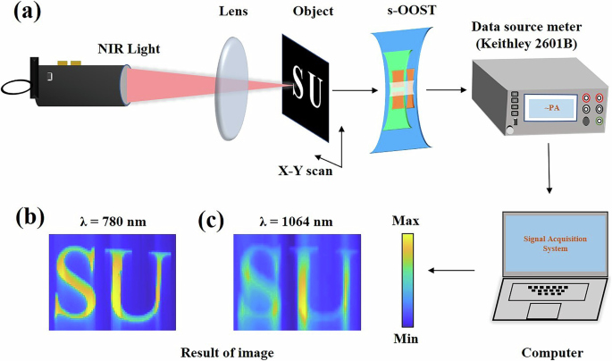
a Schematic illustration of the NIR imaging system using the s-OOSTs as the sensing pixel. b Image obtained from the 780 nm NIR imaging system. c Image obtained from the 1064 nm NIR imaging system.
Self-adaptive image memory, polychromatic optical communication and security
The s-OOSTs can be used for image recognition and memory. The “learning-forgetting-relearning” behaviors under light (365-1050 nm) stimulation were performed by applying different periods of successive light pulses to the s-OOSTs. Figure 6a shows the levels of ΔPSC under “learning (50 successive pulses of light)-forgetting (removing the light for ~50 s)-relearning (20 successive pulses of light)” process with different wavelengths. After a period of learning by applying 50 successive pulses of light (t = 200 ms, Δt = 200 ms), the ΔPSC increased to 20.6 nA (365 nm), 14.73 nA (465 nm), 10.5 nA (520 nm), 5.54 nA (620 nm), 3.41 nA (850 nm) and 2.38 nA (1050 nm), respectively. After removing the light, the ΔPSC decreased and gradually stabilized. It reflects that the s-OOSTs have good memory ability for light signals. After the relearning period with much fewer pulses (20 successive pulses of light), the s-OOSTs reached a higher ΔPSC than that after the first period of learning strength, indicating that the s-OOSTs have certain associating and relearning ability under light regulations. Moreover, after the relearning period, the forgetting time increased to > 60 s. This indicates that the s-OOSTs can reduce the learning time and increase the memory time through training. As the wavelengths of the stimulating light increased, both of the ΔPSC and forgetting time increased, revealing that increasing the wavelength can reduce the learning time and enhance the memory ability. The similar learning results were found under 50% strain (Supplementary Fig. 25). Unlike the “Learning-forgetting-relearning” behavior under electrical pulse stimulation (Fig. 3a, b), which is caused by the slow ion migration in the ion-gel, the “learning-forgetting-relearning” behavior under light stimulation arises from the slow ICT process between donor and acceptor of the PTDPPSe-6Si semiconductor45,64. Therefore, the nonvolatility of the s-OOSTs under light pulse stimulation mainly depends on the ICT relaxation in the semiconductor itself.
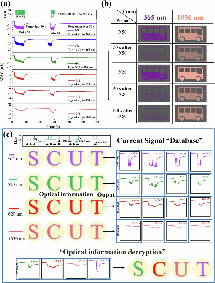
a Learning-forgetting-relearning” behaviors under different light stimulations. b Simulated bus images under 365 nm and 1050 nm light, respectively, demonstrating distinct learning, forgetting and relearning behaviors. c The application of the Morse Code “encryption” and “decryption” of the s-OOSTs.
The attenuations of the normalized ΔPSC in Fig. 6a were mapped to the changes of brightness of the images of a “bus”. Firstly, the ΔPSC was normalized according to the maximum value of ΔPSC after triggered by 50 pulses of light, and the normalized ΔPSC was recorded to form the original “bus” image (Fig. 6b, N50). Then, the shapes of the “bus” image (ΔPSC) were recorded again after first period of 50 s forgetting (50 s after N50), relearning period of 20 pulses of light (N20), second period 50 s forgetting (50 s after N20) and 100 s forgetting (100 s after N20), respectively. For the 365 nm UV light stimulation, after first period of 50 s forgetting, the image became obscure. After 20 pulses of relearning, the image became clear again, even more clear than that after first N50 learning period. After second period of 50 s forgetting (50 s after N20), the image became obscure again, but more clear compared with that after the first forgetting period (50 s after N50). Prolonging the second period of forgetting time to 100 s, the image became a little more obscure, but could still be identified.
It is worth noting that the self-adaptive image learning and memory ability of the s-OOSTs under 1050 nm NIR light stimulation was much better than that under 365 nm UV light stimulation. After relearning period under 20 pulses of 1050 nm NIR light, the image became much more clear than that after first learning period of N50. And the image was still clear even after 100 s forgetting. The self-adaptive image learning and memory abilities of the s-OOSTs under light stimulation with other wavelength are shown in Supplementary Fig. 26a. The 850 nm NIR light stimulated devices had the best image learning and memory ability, while the 365 nm UV light stimulated devices had the poorest image learning and memory ability, which is in consistence with the above PPF results (originated from the D-A ICT process). Similar results can be found under 50% strain (Supplementary Fig. 26b). This phenomenon implies that the s-OOSTs may have the ability to indentify the wavelengths of light, which is of great significance for visual adaptive sensing of an object with different colors. To demonstrate the potential application of the s-OOSTs in optical information processing and optical communication, presynaptic light pulses representing Morse codes were employed to obtain the ΔPSC responses to English letters. During the test, the pulse widths of the short signal and long signal were set to 200 and 1000 ms, respectively. The pulse interval of the same letter is 200 ms. Figure 6c represents the ΔPSC responses of the unstretched s-OOSTs triggered by the Morse code of the letters “S”, “C”, “U” and “T” with light wavelength of 365 nm, 520 nm, 620 nm and 1050 nm, respectively. The ΔPSC responses of the 50% stretched s-OOSTs triggered by the Morse code of the letters is shown in Supplementary Fig. 27. Every letter displayed a distinct ΔPSC response under different-wavelength light pulse, even under 50% strain. Finally, a group of light message composed of different light wavelengths (colors) “S”, “C”, “U” and “T” was interpreted. Compared with the traditional photoelectronic synaptic transistors, the s-OOSTs have the wavelength identification ability (that is, “color” identification ability) that can further improve the “encryption” and “decryption” security for the optical communication. This property demonstrates that our s-OOSTs have great potential in applications polychromatic optical communication and optical information security for the stretchable artificial vision systems, and may eventually make a breakthrough in the next generation of intelligent neuromorphic sensing/computing-in-memory integrated systems.
Discussion
In summary, a broadband (365–1050 nm) responsive s-OOST based on intrinsically stretchable, high-mobility, narrow-bandgap, high-relaxation-time organic semiconductor (PTDPPSe-6Si) was constructed to achieve brain-inspired memory/computation and retina-inspired visual perception/adaptation. The s-OOSTs exhibited high transconductance (86 mS) at a low voltage (−1 V) and could stand against 50% multidirectional strain. Its notable channel current brought high-density non-volatile multi-conductance states that were suitable for neuromorphic computation. Furthermore, the s-OOSTs can be stimulated by the light from ultraviolet (UV) to near-infrared (NIR) (365 nm–1050 nm), which is the widest wavelength response ever report. The relaxation time of the s-OOSTs changes greatly with the wavelengths of the incident light, making the devices possess additional abilities of light plasticity, color identification and visual self-adaptation similar to human retina. Moreover, synaptic performance was investigated at low temperature and vacuum condition. The broadband spectrum response makes it successfully image the letters “SU” in NIR environment with high contrast ratio in a single-pixel scanning imaging system, which verifies the feasibility for near-infrared sensing and visual response of the single s-OOST devices. Finally, multi-wavelength (365nm-1050 nm) optical synaptic plasticity was investigated for the imaging memory, polychromatic optical communication and information security. A series of “bus” images and letters (coded by wavelength) with different colors were identified and memorized by the s-OOSTs. The work paves a way for constructing an artificial system with dual modes of neuromorphic computation and visual perception, which are important for the next generation of intelligent sensing and computing-in-memory integrated systems.
Methods
Preparation of dextran sacrificial layer
The dextran solution was prepared by adding 1 mg dextran powder (Macklin, average Mw 20,000) to 20 ml deionized water, then heating to 60 °C and stirring for 6 h. The thermoplastic polyurethane/dimethylformamide (TPU/DMF) solution was prepared by adding 1 mg TPU (Macklin, C80 A) to 4 mg DMF (Sigma-Aldrich, 98%) solution, then heating to 80 °C and stirring for 8 h. Firstly, the glass substrate was treated by oxygen plasma for 10 min to obtain a hydrophilic interface. The dextran solution was spin coated onto the substrate at a speed of 1000 rmp to form a 200 nm dextran film as a water-soluble sacrificial layer. Then, the TPU solution was scarped onto dextran film surface to form a 200 μm TPU film as a substrate.
Preparation of ion-gel
Material
Acrylamide (AAm, 99%) and 2-Hydroxy-4’-(2-hydroxyethoxy)-2-methylpropiophenone (Irgacure 2959, 99%) were purchased from Shanghai Titan Scientific Co., Ltd. 2,2,2-Trifluoroethyl acrylate (TFEA, 98%) was purchased from Shanghai Qinba Chemical Co., Ltd., China. 1-Ethyl-3-methylimidazolium bis(trifluoromethylsulfonyl)imide ([EMIM][TFSI], 98%) was obtained from Monils Chemical (Shanghai) Co., Ltd., China.
Fabrication
The ion-gel was prepared by mixing 0.23 g AAm (Shanghai Titan Scientific Co., Ltd., 99% purity), 1.03 g TFEA (Shanghai Titan Scientific Co., Ltd., 98% purity), 1.89 g EMIM-TFSI (Monils Chemical (Shanghai) Co., Ltd., China) and 2 mg photoinitiator, and stirring thoroughly to obtain a uniform solution. Then pouring the solution onto the substrate, and irradiating it under an ultraviolet lamp for 2 h to obtain intrinsically stretchable ion-gel dielectric layer.
Preparation of the s-OOSTs
Firstly, PTDPPSe-6Si was dissolved in chloroform (5 mg mL−1) and was spin-coated on TPU substrates at 2000 rpm for 40 s. Then the polymer film was subsequently annealed at 100 °C for 30 min under nitrogen. The MWCNT was purchased from Xianfeng Nano Co., LTD., with a diameter of 20–40 nm, length > 5 μm, and a mass fraction of 10 wt.%. Then MWCNT film (150 nm) was patterned by spraying with MWCNT solution through a shading mask to form the source/drain electrodes and the side gate electrode. The channel width was 1000 μm and the length was 300 μm.
Electrical and mechanical performance testing
The s-OSSTs were characterized using a semiconductor parameter analyzer (B1500A) and a pulse generator (DG4202). The stretching test was using a flexible-tensile machine. Light source was purchased from Taiyi Optoelectronics Co., Ltd.
Responses