Gate modulation of the hole singlet-triplet qubit frequency in germanium
Introduction
Utilizing hole spin states in strained germanium (Ge/SiGe) gate-defined quantum dots for qubit operation has developed rapidly over the past several years, as groups have demonstrated fast two-qubit logic1, singlet-triplet encodings2. and a four-qubit quantum processor3. The success of these experiments can partly be attributed to the various advantages of holes for spin qubit encoding4. In stark contrast to electrons, the two topmost valence bands in Ge are well separated in energy due to strain and 2D confinement. The light effective mass (0.054 me5) of holes in the topmost band and the absence of valley degeneracy allows us to easily access the two highest hole states for spin encoding. Furthermore, Ge hole spin coherence times benefit from their weak hyperfine interaction with surrounding nuclear spins. Finally, because of their strong spin-orbit coupling and site-dependent g-tensors, Ge hole quantum dots do not require the fabrication of micromagnets, advancing their potential for scalability and integration into current industrial semiconductor facilities4.
Most double quantum dot singlet-triplet qubit studies have focused on encodings between the singlet (leftvert Srightrangle) and unpolarized triplet (leftvert {T}_{0}rightrangle) states2,6,7,8. In this work, we detail the dynamics of the S − T_ subspace, which has been less studied thus far9,10,11. Furthermore, we explore the tunability of the hole g-tensors by varying the electrostatic potential generated by the barrier gate bridging the two quantum dots. As quantum computation with Ge hole spins critically depends on the g-tensor, the ability to manipulate the g-tensor becomes a valuable asset for a spin qubit encoded in this system.
Results
Singlet-triplet evolution in a DQD
A scanning electron microscope image of the device studied is shown in Fig. 1a along with the Ge/SiGe heterostructure and metal gates in Fig. 1b. The strained Ge quantum well is 16 nm in width and located 55 nm below the surface. For more details regarding the heterostructure, see ref. 5. A two-dimensional hole gas is first created in the Ge well by applying a negative voltage to a global top gate situated above the heterostructure. The double quantum dot (DQD) is then formed underneath plungers P1 and P2 by applying appropriate voltages to the neighboring barrier gates, where the middle barrier voltage VB controls the coupling between the two dots. Varying the plunger voltages controls the chemical potential of each dot, allowing us to reach the few-hole regime (Fig. 1c), where all experiments were performed at the (1,1)-(0,2) anticrossing (Fig. 1d). The hole occupation of both dots was detected by the nearby SET (left half of the device) labeled in Fig. 1a. For convenience in describing this DQD system, we define the relative energy of the two quantum dots as the detuning ε = eα2VP2 − eα1VP1 where αi converts the voltage applied to Pi to the change in the energy levels between the two dots. Figure 1d illustrates the detuning axis on the stability diagram, where we define ε = 0 at the (1,1)-(0,2) boundary.
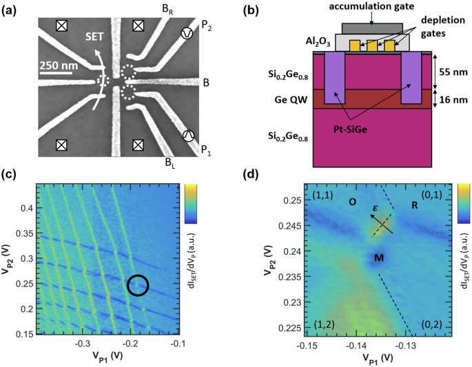
a SEM image of lithographically defined gates identical to the device used in this study. b Heterostructure of the device showing the Ge quantum well packed between two Ge rich SiGe layers. Ti/Au depletion gates are deposited on top along with an Al global accumulation gate. c A typical stability diagram with the circle highlighting the (1,1)-(0,2) anticrossing. d All experiments were completed at the (1,1)-(0,2) anticrossing, where (n,m) denotes the hole occupation for each dot. Point R was used to reset the DQD, M for measurement and initialization, and O for coherent operation between the singlet and triplet states.
When the system passes the ε = 0 detuning line into the (1,1) charge configuration, the (0,2) singlet state hybridizes with the (1,1) singlet due to the tunnel coupling between the quantum dots: (leftvert Srightrangle =sin left(Omega /2right)leftvert {S}_{02}rightrangle -cos left(Omega /2right)leftvert {S}_{11}rightrangle). Here, ({scriptstyleOmega} =arctan left(frac{2sqrt{2}{t}_{c}}{varepsilon }right)) is the mixing angle between the two singlet states. In addition to (leftvert Srightrangle), Fig. 2c depicts the three triplet states that compose the four lowest energy levels in the (1,1) charge configuration. A simple block magnet situated near the device’s PCB provided the field necessary to lift the degeneracy of the three triplet states, generating an estimated fixed global out-of-plane field of 1.2 mT and in-plane field of 4.4 mT measured at the device’s position (∣B∣ = B = 4.6 mT points θ = 15° out of the x-y plane). This tilted field differs from previous qubit experiments on this heterostructure where B was completely in-plane, allowing for a unique perspective into the hole spin states3,11. Importantly, this magnetic field splits the polarized triplet (leftvert T_rightrangle) from (leftvert {T}_{0}rightrangle) by the average Zeeman energy of the quantum dots ({overline{E}}_{z}).
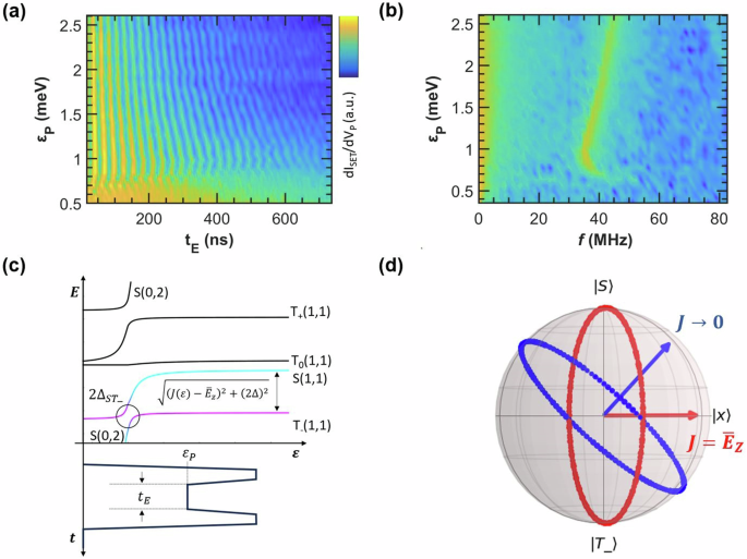
a The SET signal as a function of the detuning and evolution time, illustrating coherent oscillations between (leftvert Srightrangle) and (leftvert T_rightrangle). The chevron pattern located near 1 meV arises from the S − T_ anticrossing defined by the energy splitting ΔST_, while oscillations at large detunings are controlled by the average Zeeman energy of the two dots: ({overline{E}}_{z}). b Fourier transform of the coherent oscillations in (a), illustrating the S − T_ energy splitting as a function of detuning. c Energy levels (not to scale) of the singlet and triplets as a function of detuning. The Ramsey pulse used is shown below as a function of time and detuning. d Bloch sphere depicting the two rotation axes for the S − T_ subspace. When εP is at the S − T_ anticrossing, the system undergoes X rotations (red axis). For large detunings, a combination of X and Z rotations are performed (blue).
Beginning at M in Fig. 1d, the system is first initialized into the (0,2) singlet state. A voltage pulse was then applied to P1 and P2 to quickly separate the holes and create a small admixture between the (1,1) singlet ({scriptstyleleftvert Srightrangle} =frac{1}{sqrt{2}}(leftvert uparrow downarrow rightrangle -leftvert downarrow uparrow rightrangle )) and polarized triplet (leftvert T_rightrangle =leftvert downarrow downarrow rightrangle) states. Once the holes were separated, the system was pulsed to various operation detunings εP and allowed to evolve for a time tE between (leftvert Srightrangle) and (leftvert T_rightrangle) (Fig. 2a, c). We use εP to refer to the change in detuning applied by the pulse, which is offset from ε by the readout position (εr) at point M: ε = εP + εr. The qubit frequency (Fig. 2b) is given by the energy difference between these two states at the operation detuning: hf = ΔEST_, which plateaus to roughly ({overline{E}}_{z}) for large detunings.
For smaller operation detunings, the energy splitting reaches a minimum at the S − T_ anticrossing, where it approximately equals 2ΔST_. We define ΔST_ as the coupling between (leftvert Srightrangle) and (leftvert T_rightrangle) at the S − T_ anticrossing. By varying the operation detuning εP from 0.5 to 2.5 meV, we sampled the energy splitting between the two lowest states for both regimes. The existence of this minimum leads to the observed chevron pattern at 1 meV in Fig. 2a, which has been seen in previous S − T_ works and absent from studies coherently manipulating the S − T0 states2,6,7,8,9,10,11.
To understand these dynamics, we utilize a Hamiltonian describing the ({leftvert Srightrangle ,leftvert T_rightrangle }) subspace that was derived in ref. 12 and is a reduced form of the full model used in ref. 9. To leading order, it takes the following form:
We define the exchange energy ({scriptstyle{J}(varepsilon)}=-frac{varepsilon}{2}+sqrt{frac{{varepsilon }^{2}}{4}+2{t}_{c}^{2}}) as the energy difference between (leftvert Srightrangle) and (leftvert {T}_{0}rightrangle). The coupling of the S − T_ states (Δ) emerges from two sources: a spin-flip tunneling process induced by the spin-orbit interaction (Δso) and the anisotropy of the g-tensors (ga) that is primarily determined by the difference of in-plane g-factors: (Delta =| {Delta }_{so}sin left(frac{Omega }{2}right)+{g}_{a}{mu }_{B}Bcos left(frac{Omega }{2}right)|)9,12. The anisotropy between the in- and out-of-plane g-factors of a quantum dot has been previously observed, where the in-plane g-factors (g∥) were measured to be a few tens to hundreds of times smaller than their out-of-plane counterparts (g⊥) for holes in Ge/SiGe substrates9,13. The (leftvert T_rightrangle) state splits from (leftvert {T}_{0}rightrangle) by the average Zeeman energy, ({overline{E}}_{z}=overline{g}{mu }_{B}B), where (overline{g}) is the average g-factor of the two dots projected onto the axis of B.
With this Hamiltonian, we can solve for the frequency of the S − T_ evolution: ({scriptstyle{f}}=frac{1}{h}sqrt{{(J-{overline{E}}_{z})}^{2}+{(2Delta )}^{2}}). At the S − T_ anticrossing, (J={overline{E}}_{z}), and f is controlled by Δ, where X rotations are performed around the Bloch sphere (Fig. 2d). For large detunings, J → 0, leaving f to be determined by the average Zeeman energy and S − T_ coupling, and the qubit rotates near the z axis. The larger the ratio (frac{{overline{E}}_{z}}{Delta }) becomes, the closer this axis aligns with the z direction. We note that with control over the orientation of the magnetic field, it is possible for Δ → 0 at specific detunings, resulting in perfect Z rotations12.
After manipulation, the separated holes were reunited in the (0,2) charge configuration at M for spin readout of the final state using Pauli spin blockade. The system is then reset at R before repeating the cycle again. For a detailed explanation of each step of the pulse, see the Supplementary Material.
Dephasing and relaxation
We first analyzed the dephasing and relaxation of this qubit by measuring ({T}_{2}^{* }) and T1. For each εP in Fig. 2a, the S − T_ evolution was fit to a Gaussian damped sinusoid (P=A{e}^{-{(t/{T}_{2}^{* })}^{2}}cos (omega t+B)+C{e}^{-t/D}+E), where ({T}_{2}^{* }) is the inhomogeneous dephasing time. For example traces and details relating to this fit, see the Supplementary Material. After extracting ({T}_{2}^{* }) as a function of εP (Fig. 3a), a clear dependence on the pulse height is seen. This behavior can be understood with a simple model describing the influence of charge and magnetic noise on the fluctuations in the energy difference between the two states2,6:
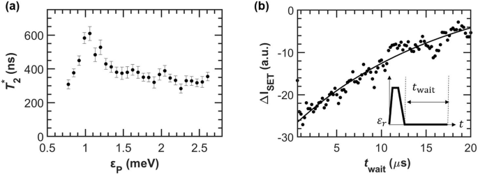
a ({T}_{2}^{* }) as a function of detuning. Linecuts in Fig. 2a are fit to the curve ({P}={{A}{e}^{-{(t/{T}_{2}^{*})}^{2}}}{rm{cos}} ({{omega}{t}+{B}})+{{C}{e}^{-t/D}+E}), where the dephasing time ({T}_{2}^{* }) is extracted and plotted in (a). Error bars equal one standard deviation of the uncertainty in ({T}_{2}^{* }) from this fit. This decoherence can be understood as a contribution from two noise terms with the simple model shown in Eqn. (2). From this model, we estimate δΔrms = 0.8 and (delta {overline{E}}_{z,text{rms}}=3) neV. b A T1 measurement where the change in SET current is recorded as a function of wait time at the measurement point M. We extract T1 from the fit (P=A{e}^{left(-t/{T}_{1}right)}+B) (solid line) and calculate T1 = 17.2 ± 3.2 μs. Inset: the pulse used to observe this decay.
At the S − T_ anticrossing where the qubit frequency reaches a minimum, the system is insensitive to first-order to fluctuations in ε due to charge noise. This protection leads to the maximum in ({T}_{2}^{* }) seen at 1 meV in Fig. 3a. However, the qubit is still susceptible to electrical noise affecting the dot g-factors and tunnel coupling as well as magnetic noise afflicting B. We can estimate the magnitude of this noise combination from Eqn. (2) using the fact that (J={overline{E}}_{z}) at this detuning. Under this condition δE = 2δΔrms, where we define δΔrms to include the noise sources pertinent to tc, ga, and B, leading to
For large operation detunings, the energy separation between the S − T_ states reaches a parallel regime (Fig. 2b), which diminishes the charge noise contribution to δE. In this regime, ΔEST_ approximately equals ({overline{E}}_{z}), where the combined electrical and magnetic “Zeeman” noise affecting (overline{g}) and B limits ({T}_{2}^{* }). We estimate this parameter using Eqn. (2) again:
In general, the T1 spin relaxation time is known to be orders magnitude longer than ({T}_{2}^{* }) in Ge-based semiconductor QDs at the operation point1,3,14, and we believe this system is similarly limited by ({T}_{2}^{* }). However, to determine adequate integration times for the projective measurement at the (2,0) readout point εr, the system’s T1 at εr was measured by varying the wait time at εr (Fig. 3b). For these measurements, the system was allowed to completely dephase at the operation detuning εP before being pulsed back to the readout window for a variable amount of time (see inset of Fig. 3b). We fit the resulting exponential decaying curve shown in Fig. 3b to (P=A{e}^{-(t/{T}_{1})}+B) and find T1 to be 17.2 ± 3.2 μs, which is comparable to experiments done in S − T0 qubits2.
Gate modulation of the singlet-triplet frequency
We now focus on modulating the coherent evolution of the S − T_ states by adjusting the voltage applied to the barrier separating the two quantum dots. Over a 22 mV range in voltage, Fig. 4 illustrates the dramatic transformation the S − T_ oscillations undergo. As the middle barrier voltage VB is increased, the S − T_ oscillation frequencies undergo an interesting shift seen in Fig. 4. The frequencies in the entire detuning span decrease from VB = −60 mV to −48 mV before oscillations are no longer visible at VB = −46 mV. However, as VB is continuously pushed to more positive values past VB = −46 mV, the oscillations return and now increase with VB. From the Fourier transform of these oscillations, we can isolate two quantities of interest, namely (overline{g}) from the frequency at large detuning following (f sim {overline{E}}_{z}/h) and ΔST_ from the minimum frequency near εP = 1 meV, where f = 2ΔST_/h.
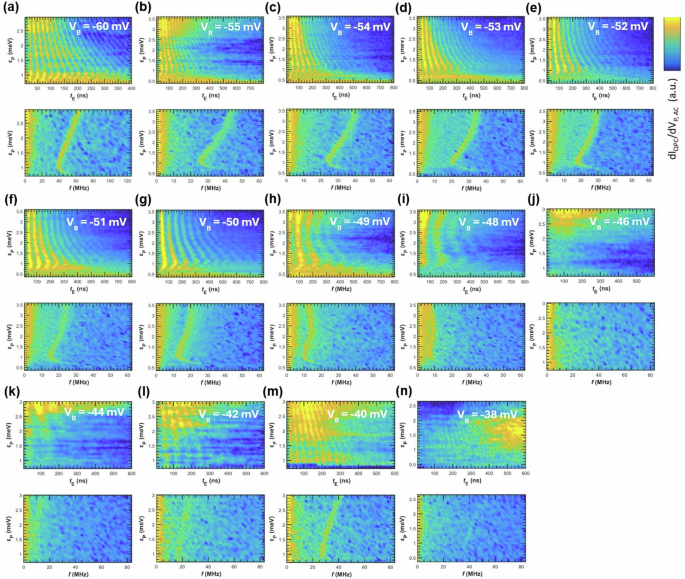
a–n The upper panel depicts S − T_ oscillations, while the lower panel shows their corresponding FFTs. Applying a more positive barrier gate voltage decreases the frequency of the oscillations throughout the entire detuning range until VB = −46 mV. Afterwards, the frequencies reverse direction and increase. The minimum and maximum frequencies correspond to ΔST_ and (overline{g}).
We would like to note that the location of the frequency minimum ε* is determined by the tunnel coupling tc and ({overline{E}}_{z}) from the condition (J={overline{E}}_{z})9:
Because ε* remains approximately constant throughout this range of VB, a decrease in tc must be accompanied by a decrease in ({overline{E}}_{z}). While it is evident from the sharper rises seen in the FFTs of Fig. 4 that tc changes with VB, a similar change in ({overline{E}}_{z}), and therefore (overline{g}), is necessarily present. The existence of this minimum frequency marking where (J={overline{E}}_{z}) also serves the purpose of justifying (J < {overline{E}}_{z}) at larger detunings. In this regime, the average Zeeman energy plays the major role in determining the S − T_ evolution frequency. Therefore, we can use the frequency at large εP in Fig. 4 to extract the dependence of (overline{g}) on VB.
Discussion
Figure 5 captures the main experimental findings of the paper. From the analysis described above, we find both ΔST_ and (overline{g}) strongly depend on the gate voltage of the barrier gate VB. Both quantities can be varied nearly an order of magnitude with a modest voltage adjustment of around 12 mV. In addition, interestingly enough, both ΔST_ and (overline{g}) can either increase (for VB >−48 mV) or decrease (for VB >−48 mV) as a function of VB. The observations show that the qubit frequency can be modulated considerably by a single gate. On the one hand, it provides an effective means to electrically control the singlet-triplet qubit frequencies, on the other hand, it shows that the qubit is susceptible to a small variation of the gate-voltage. In either case, it would be useful to understand the mechanism of such gate voltage modulation.
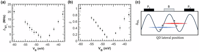
a ΔST_ as a function of barrier voltage. Values are extracted from the minimum frequency of the FFTs shown in Fig. 4. b (overline{g}) is extracted from frequency at large detunings in Fig. 4 and plotted versus the barrier voltage. Both parameters show a strong dependence on the barrier gate voltage. This behavior can be explained by the dots moving through a non-uniform strain environment, which directly impacts the g-factors of each dot. Error bars for (a) and (b) are calculated from the linewidth of the Fourier transform data. c Cartoon depicting the ΔHL profile underneath the confinement gates due to the effects of strain.
In the literature, a leading mechanism for g-factor changes in Ge quantum dots are accomplished through altering the admixture of light-hole (LH) states into the predominantly heavy-hole (HH) ground state of the Ge quantum dot. While it is well known the upper valence bands in Ge/SiGe heterostructures are composed primarily of HH states due to a large HH-LH splitting ΔHL4, an accurate understanding of the g-tensor in many Ge materials requires the consideration of the LH bands9,15,16,17,18,19,20,21. To understand the consequences of this mixing, it is beneficial to first examine the g-factor components of both bands in the case of 2d confined holes in Ge. As described in refs. 16,20,22,23, for the pure HH state, the out-of-plane g-factor is ({g}_{perp }=6kappa +frac{27q}{2}) and the in-plane component is g∥ = 3q, where κ = 3.41 and q = 0.07 are the magnetic Luttinger parameters. Note this κ and q result in the large anisotropy of the g-tensor: g⊥ ≫ g∥. Conversely, for pure LH states, g⊥ = 2κ and g∥ = 4κ. Comparing these two bands, the LH state has a smaller g⊥ but greater g∥ relative to the HH state. Therefore, when increasing the LH admixture in the ground state of the quantum dot, we expect a decrease in g⊥ and an increase in g∥, which has been experimentally observed for various mixing mechanisms9,16,17,23.
As discussed, ΔST_ can be altered either by the spin-flip tunneling strength (Δso) or the anisotropy term (ga) that primarily relies on the difference of in-plane g-factors between the two quantum dots. One expects the spin-flip tunneling process to continuously decrease as the dots are pushed further apart by VB24,25. Since we observe that ΔST_ can either increase or decrease as a function of VB, we assert ga is responsible for the change in ΔST_. Additionally, ΔST_ following the same trend as (overline{g}) points to a common mechanism underlying both behaviors.
Due to the large anisotropy between g⊥ and g∥, (overline{g}) is dominated by its out-of-plane component ({overline{g}}_{perp }). With an increase in HH-LH mixing, we then expect a decrease in (overline{g}) through a reduction in g⊥ for either dot. On the other hand, the in-plane g-factors are the leading order terms defining ga, where a more similar g∥ between the two dots diminishes ga. That is, when (| {g}_{parallel }^{L}-{g}_{parallel }^{R}|) reduces, so does ga. This can be accomplished when the mixture of LH states for the left and right dot change by different amounts to bring ({g}_{parallel }^{L}) closer to ({g}_{parallel }^{R}). Importantly, this mixing of the HH and LH states can explain both trends we observe in Fig. 5.
How can a small gate-voltage change in our structure alter the HH-LH mixing and consequently the g-factors? Here we would like to discuss one possible cause where a non-uniform strain profile in our device can lead to the change of HH-LH mixing as VB is varied. This proposal is motivated by the recent experimental work of Corley-Wiciak et al.26 on a strained Ge quantum well heterostructure, similar to that used in the current experiment. Strain originates from the differences in thermal contraction between the gate electrodes defining the quantum dots and the substrate. This strain can both alter ΔHL and directly mix the HH and LH states, where these effects are greatest along the edges of the confinement gates20,26,27,28. In the scanning x-ray experiment, the strain profile of a gate-defined quantum dot device was mapped out in nanoscales, and a subsequent simulation shows that ΔHL and strain along the dot channel can vary as much as 4% and 0.03% respectively Although this percentage seems small at first glance, even increases in LH admixtures of 1% significantly reduce g⊥16.
Can such inhomogeneous strain profile produce the large g-factor modulation observed in our experiments? The recent work by Abadillo-Uriel et al.20 provides an excellent, rigorous description of the effects of strain on the g-tensor of a quantum dot. As the off-diagonal elements of the strain tensor (e.g., εzx and εzy) change, the g-factor corrections described in ref. 20 dictate how the g-tensor magnitude and orientation shift. Because the magnetic field remained fixed in this experiment, the measured g-factor will then change accordingly. Given that the magnetic field in our experiment was tilted only ~ 15° from the sample plane combined with the large g-tensor anisotropy of this system, these strain variations can significantly influence the effective g-factor. We then arrive at a reasonable qualitative picture shown in Fig. 5c: the dependence of ΔST_ and (overline{g}) on VB can be explained by adjusting the dots through a variable strain landscape, where we estimate the right dot shifts ~36 nm laterally between −60 mV and −48 mV (see the Supplementary Material). The fluctuating strain introduces variations in the light-hole admixture, which is modulated by the strain profile beneath the gate electrodes. Consequently, the measured g-factors are also affected by this modulation.
We would like to caution the reader that our arguments here are primarily qualitative, providing a potential explanation for the experimental observations. To achieve a quantitative comparison between our experimental data and theoretical predictions, finite-element simulations would be required to model the thermal contraction-induced strain profiles and their effects on the g-factor in the specific device used for this experiment. Additionally, experimental determination of material parameters related to thermal contraction and the original g-tensor-prior to accounting for the inhomogeneous strain-would be necessary.
We would like to note that in addition to strain, we have considered the deformation of the quantum dot in-plane confinement potentials as a source for the observed g-factor variation. As described in refs. 9,18, asymmetry in this potential can lead to mixing between the heavy- and light-hole states, resulting in g-factor corrections that scale with the asymmetry of the confinement strength: δgx,y ~ ∣ωx − ωy∣ and δgz ~ ∣ωx − ωy∣2 ≲ 10−2 9. While this explanation is plausible for the behavior of ΔST_ due to the already small values of the in-plane g-factors, it does not capture the large variation in (overline{g}), which is dominated by g⊥ and insensitive to elliptical confinements. Furthermore, the observation that both ΔST_ and (overline{g}) follow the same trend (decreasing until VB =−48 mV) suggests the same mechanism is responsible for both. However, we would like to stress that our intent with focusing on strain is not to rule out this and other explanations of HH-LH mixing. We rather wish to illustrate a reasonable picture that encourages the community to consider the strong variation in g-factors present.
In summary, we have explored the coherent oscillations in a Ge hole double dot between the singlet, (leftvert Srightrangle), and polarized triplet state, (leftvert T_rightrangle). The dephasing time of this manipulation strongly depends on the operation detuning with a maximum of ({T}_{2}^{* }=600) ns, while the spin relaxation time at the readout point was measured to be T1 = 17.2 μs. The maximum in ({T}_{2}^{* }) coincides with the minimum in the S − T_ energy splitting, where the system is insensitive to the noise disturbing J and ({overline{E}}_{z}). Furthermore, we observe the frequency of evolution between these spin states can be heavily modulated through the voltage of the middle barrier separating the two dots. We show a dynamic dot position over a variable strain profile is a possible explanation for the qubit’s frequency dependence on VB. These results suggest strain can be exploited to fine-tune qubit frequencies in Ge. Furthermore, if a variable frequency profile is not desired, the sensitivity of the g-tensor to the quantum dot position can be mitigated by reducing strain in the system, such as by defining gate electrodes with palladium instead of gold to closer match the thermal response of Ge29.
Methods
Device preparation
The device was fabricated on top of a Ge/SiGe heterostructure with the strained Ge quantum well buried 55 nm beneath the surface. Ohmic regions were patterned with photolithography and the wafer was dipped in buffered HF (BOE) to remove the thin capping layer of SiO2. These regions were then metallized with 60 nm of Pt through e-beam evaporation. We used e-beam lithography to pattern all device leads and a second e-beam evaporation to deposit 5/45 nm of Ti/Au. A 100 nm insulating layer of Al2O3 was grown through atomic layer deposition, and a subsequent global top gate was patterned with photolithography. This was followed by a final e-beam evaporation of 100 nm of Al to form the global accumulation gate. The device then underwent a forming gas anneal at 420 C for 1 h to repair defects in the oxide and anneal the Pt Ohmic regions into the substrate.
Measurement setup
The device was cooled in a Triton dilution refrigerator with a base temperature of 48 mK. All SET current measurements were performed with an SR 830 Lock-in amplifier. When measuring stability diagrams, the lock-in excitation voltage was applied to both plungers and the current through the SET was fed back into the lock-in for integration and demodulation. A voltage pulse to each plunger was supplied by a Tektronix AWG 610 with its pulse frequency modulated by the lock-in. With the lock-in integration time set to 100 ms, 5000 pulse sequences were averaged for each data point during the spin manipulation measurements. All measurements using the AWG pulse were made with no lock-in excitation voltage applied to the plungers. The magnet used was the model B444-N52 produced by K&J Magnetics, Inc. and attached directly next to the device’s PCB. A Hall probe measured the magnetic field at the device’s position on the PCB.
Responses