Fabrication and characterization of low-loss Al/Si/Al parallel plate capacitors for superconducting quantum information applications
Introduction
Superconducting qubits employ Josephson junctions, inductors, capacitors, and transmission lines to realize physical systems exhibiting quantum properties with discrete energy levels that can be used for computation1,2,3. Quantum computation using superconducting qubits has been shown to be possible through milestone demonstrations moving toward quantum advantage4,5. Studies demonstrating large-scale qubit integration6 have shown that superconducting qubit technology is promising, and is presently accepted as a leading candidate to achieve large-scale, fault-tolerant quantum computation7.
The Josephson junction and the reactive components of qubit circuits are made from superconductors and insulators that are dissipationless in principle; however, microscopic contamination, such as undesired oxides and residues at surfaces and interfaces, can serve as dissipation channels that cause decoherence in real systems8,9. These oxides and residues are known to host two-level systems (TLS)10, which may exchange energy with qubits and are understood to be the dominant decoherence source in many real devices11,12,13,14.
Coherence times in transmons, one type of superconducting qubit which consists of a Josephson junction shunted by a capacitor, have dramatically improved in recent years due to the integration of new materials and mitigation of surface loss15,16,17. Mitigation of surface loss through the design of the transmon geometry has proven effective, where large, planar capacitor structures are often used to dilute the participation of the surfaces and interfaces. These large (typically millimeter scale) devices tend to outperform more compact capacitor structures such as parallel-plate and inter-digitated designs18,19. However, a major disadvantage of larger planar capacitors is a reduction in scalability, both due to the increased footprint on the chip and the need to address stray fields that couple devices to other resonant modes on a chip, as well as the packaging environment20,21. In addition, these large devices have electric field energy residing at surfaces that are exposed to the ambient atmosphere and contamination sources during processing, storage, and packaging steps, which brings consistency, repeatability, and age resilience into question.
Many of these issues may be addressed by switching to parallel plate capacitor (PPC) geometries composed of superconductor/insulator/superconductor (SIS) sandwiches. PPCs offer advantages over planar capacitor geometries: the electric field energy is mostly contained in the tri-layer structure with little participation in surface regions exposed to the atmosphere, and are also inherently more compact22,23. However, having the field energy contained within the dielectric region of the sandwich places a high demand on the loss properties of the dielectric and its interfaces with the superconductor13.
Fabrication of PPCs and Josephson junctions from SIS tri-layers with deposited dielectrics or vacuum gap capacitors has been demonstrated24,25,26,27,28; however, devices made using tri-layer processes typically have high microwave loss and are not used for applications such as transmons with high coherence times. Conventional growth of planar SIS tri-layers is difficult, largely due to materials considerations in growing a high-quality dielectric on a superconducting metal. Interestingly, at the time of this writing, the best performing PPC from the standpoint of low-loss microwave performance was made by exfoliating 2-D materials rather than direct tri-layer growth29,30.
In this work, an alternative approach is used to create parallel plate capacitors by etching the capacitor dielectric out of Si substrates31, which has been established as one of the lowest loss dielectrics available32. The process presented in this work takes advantage of the highly anisotropic crystallographic etching of Si(110) substrates with potassium hydroxide (KOH) to form high-aspect-ratio fin structures with flat Si{111} sidewalls which are contacted with aluminum to form the PPC. Using Si(110) substrates to fabricate fins having Si{111} sidewalls allows high aspect ratio structures to be fabricated without the need to develop anisotropic dry etch processes optimized for low microwave loss. Moreover, the Si(111) surface is known to be desirable for the growth of high-quality epitaxial aluminum33. Here, Si fins have been incorporated as the capacitive element in both lumped element resonators and transmons. We find that the Si fins are high performing with figures of merit including low power internal quality factor (Qi) of lumped element resonators, qubit quality factor, and qubit T1 times meeting or exceeding the state-of-the-art for comparable devices mad`allel plate capacitor technology.
Methods
Lumped element resonator and transmon design
Frequency multiplexed lumped element resonator chips and transmon chips with multiplexed readout resonators were fabricated on the same 50.8 mm wafer. Having both resonator and transmon chips fabricated together allows for independent characterization of the Si fin PPC and the transmon. 3D simulations of the resonators and qubits were performed using finite element analysis.
The lumped element chip design consists of 8 resonators inductively coupled to a central feedline that is measured in the hanger configuration. Each lumped − element resonator consists of a metalized section of a Si fin (capacitor), which is shunted by a 15 μm wide Al thin-film wire inductor having an inductance of 4.29 nH and stray capacitance of 84.1 fF determined by simulation. For the devices presented here, 81−84% of the total capacitance of each lumped element resonator is from the fin capacitor. The frequency of the resonators is controlled by lithographically incrementing the metalized length along the fin capacitor, which is linearly related to the device capacitance.
The transmon chip layout consists of 6 nominally identical transmon qubits coupled to frequency multiplexed readout resonators. Devices were designed to employ Si fin parallel plate capacitors shunted by Josephson junctions. The transmons were designed to have anharmonicities α/2π = 300 MHz, qubit-readout coupling constants g/2π = 100 MHz, and EJ/EC = 50. While this design was not made to minimize areal footprint, the approximate footprint is 0.01 mm2, significantly lower than the footprint of commonly used capacitor designs optimized for high coherence times which typically fall in the range of 0.2–0.5 mm2 with some designs even exceeding 1 mm2 19[,34.
The readout resonators are quarter − wave coplanar waveguide (CPW) resonators inductively coupled to a central feedline and capacitively coupled to the fin transmons. In this design, both the coupling capacitance and the transmon capacitance are realized using metalized sections of the same Si fin, demonstrating the convenience of the Si-fin process to construct capacitive elements.
Device fabrication
Fin capacitors are fabricated on Si(110) substrates using a combination of dry and wet etching closely following the process outlined in a previous work31. As-received substrates were cleaned before LPCVD growth of 100nm low-stress silicon nitride (SiNx) that serves as a hard mask. The fins are patterned using electron beam lithography(EBL) and a negative resist followed by dry etching to pattern the LPCVD nitride. The fin patterns are aligned so that the long axis of the fin is parallel to the major flat of the Si(110) wafer, which is critical to obtain the desired flat {111} sidewalls and high aspect ratio structures.
After resisting stripping and wafer cleaning, the wafer was immersed in a solution of 45% KOH (by weight) in water held at 87 °C for 2 minutes to anisotropically etch the Si. This procedure results in approximately 3 μm etching into the substrate with approximately 40 nm of undercut on each side of the SiNx hard mask. The resulting fin structure consists of a 2.2 μm tall parallel-plate region having uniform thickness near 220 nm with flat Si{111} sidewalls and a tapered base region having an approximate height 0.8 μm. The tapered base region of the fin forms naturally as a result of the anisotropic etch and may enhance its structural stability.
Dry etching processes e.g. the Bosch process, may also be used to generate high aspect ratio silicon structures35, though resulting sidewall contamination and structural damage may be sources of microwave loss. The simple wet etch procedure employed here circumvents the need to develop dry etch processes for low microwave loss while allowing for a self-aligned deposition to isolate the capacitor plates using the undercut on each side of the SiNx hard mask.
Following the formation of the Si-Fin capacitors, the wafer was cleaned with solvents, and the silicon native oxide was removed with a buffered oxide etch (BOE). After the BOE etch, the wafer was rinsed in DI water before immediately loading in a high vacuum for aluminum deposition. Aluminum was deposited in two 50 nm thick depositions at ± 25° from the wafer surface normal and aligned to coat the sides of the fins. This procedure results in 100 nm of aluminum metal deposited on the wafer surface and 50 nm on the sides of the fins. The undercutting of the fins below the SiNx hard mask was used to shadow the aluminum during deposition to form a self-aligned break in the metallization near the top of the fins. Transmission and scanning electron micrographs which clearly show this self-aligned break in the aluminum layer near the tops of the fins are included in the prior work by Goswami et al.31.
Following aluminum deposition, the metal layer was patterned using optical lithography and wet etching. A standard spin-on photoresist was used, using a spin process that results in a layer thickness of approximately 1 μm on an unpatterned wafer. On wafers with patterned fins, the resist profile is nonuniform near the fins due to the topography. In order to accurately transfer patterns onto the wafer, extra exposure doses were applied near the fins as needed to clear resist residue. After photolithography, the 100 nm thick Al layer was wet-etched using a phosphoric and nitric acid-based aluminum etchant at room temperature. Notably, the SiNx hard mask and the Al layer deposited on top of it were not removed from the fins. Microwave measurements of SiNx have shown the material to have several orders of magnitude higher loss than pure silicon14,36, so it is expected to contribute loss channels in these devices as well.
Al/AlOx/Al Josephson junctions were deposited using a standard EBL/Dolan bridge process37 employing a PMMA/PMGI bi-layer. The target dimensions of the junctions was 100 nm x 100 nm. As previously stated, resist profiles are nonuniform in proximity to the fin capacitors, so junction dimensions were calibrated on a separate wafer by patterning junctions at varying distances from the ends of the fins and measuring dimensions with atomic force microscopy. It was found that placing junctions at distances greater than 30 μm from the ends of the fin resulted in reproducible junction dimensions within 10% of the targeted values.
Following EBL exposure and development, the wafer was loaded in an electron beam evaporator for Josephson junction deposition. Prior to bottom electrode deposition, the exposed areas of the wafer were ion milled to remove native oxide from the Al metallization layer and create transparent contacts to the junction. A 35 nm thick bottom electrode was deposited at + 14. 7°, oxidized at 180 mTorr in pure O2 for 10 minutes to form the tunneling barrier, followed by deposition of the 75 nm thick bottom electrode at −14.7°. After junction deposition, protective photoresist was spun on the wafer which was diced down to 7.5 mm x 9.5 mm die. Individual chips were then selected and the aluminum layer from junction deposition was lifted off. The finished junctions measured after dicing had room temperature resistances near 9.3 kΩ suggesting an approximate junction critical current of 30 nA and Josephson inductance of 11 nH. Figure 1 shows optical micrographs and circuit schematics for both the lumped element resonator and transmon devices as well as a scanning electron micrograph of a fabricated transmon.
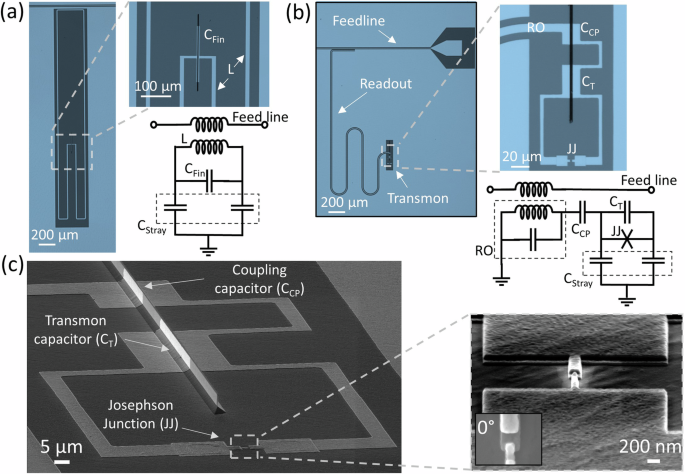
a, b Optical micrographs and corresponding circuit schematics for Si-fin lumped element resonators and transmons respectively. The functional components of the fin transmon are indicated and illustrate the capacitive coupling of the fin transmon to the readout resonator (RO). c Scanning electron micrograph of a Si-fin transmon. The insets show the Josephson junction region in higher magnification.
Measurement setup
After lift-off, cleaned chips were wire-bonded with aluminum wire and packaged in a 2-port package constructed of Au-plated OFHC Cu for low-temperature RF measurements. All microwave measurements were performed in a dilution refrigerator having a base temperature of 35 mK. The attenuation and amplification setup used for both resonators and qubits is similar to that presented by McRae et al.14. Lumped element resonators were characterized using a vector network analyzer (VNA) by fitting the power-dependent S21 spectra of the resonators using the diameter correction method (DCM)14,38. Qubits were measured in the time domain using QICK software running on a Xilinx/AMD ZCU216 RF SoC board with a measurement configuration similar to that presented by Stefanazzi et al.39.
Results and Discussion
Figure 2a shows the measured resonant frequency of the lumped element resonators as a function of metallized length along the Si fins. The data suggests the expected linear dependence of ({(1/{f}_{r})}^{2}) on capacitor length. Given the inductance value of 4.29 nH determined from simulations, the slope of the interpolated line may be used to estimate the capacitance per unit length (C0) of the fin structures which is found to be 2.1 fF/μm. Extrapolating the linear fit to zero fin length (L = 0) gives a resonant frequency of 8.97 GHz, in reasonable agreement with simulation results yielding a self-resonance of the inductor loop at 8.3 GHz.
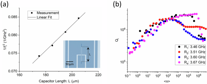
a Measured resonant frequency vs metallized capacitor length (L) for LERs. The inset includes an optical micrograph of a device with the dimension L indicated. Electromagnetic simulations of the inductor loop suggest that the fin structure contributes 81–84% of the total resonator capacitance. b Extracted internal quality factor (Qi) plotted against the estimated photon number in the cavity of the four resonators measured in (a).
A crude parallel plate approximation of fin capacitance using the measured fin height and width of 2.2 μm and 220 nm, respectively, yields ≈ 1.0 fF/μm for a silicon dielectric constant of 11.7. This significantly lower value reflects the contribution of stray and additional capacitance near the base of the fin to the total capacitance of the structures. Notably, the electric fields from metallization at the base of the fin are predominantly contained in the Si substrate rather than at the material surfaces.
Power-dependent S21 of the lumped element resonators was also measured and is included as Fig. 2b. Internal and coupling quality factors (Qi and Qc) were extracted from the S21 data, and the cavity photon number was then estimated using Qi, Qc, and the measured input line attenuation.
Referring to Fig. 2b, the lumped element resonator Qi reaches a maximum at intermediate powers and anomalously decreases with increasing power. This effect is attributed to Cooper-pair breaking in the superconducting aluminum14,40 at higher RF drive power and has been reported before in similar structures30. Qi values near the single photon level are observed to be very good, with several points exceeding 500 k, which, to the authors’ knowledge, is the current state-of-the-art for superconducting resonators made using parallel plate capacitors30.
All 6 qubits on the separate transmon chip were found to be functional, and characterization results are included as Table 1. Anharmonicity (α) was computed using the measured values of f01 and f02/2 obtained from continuous-wave qubit spectroscopy measurements. f01 and f02 denote the frequencies corresponding to the 0 → 1 and 0 → 2 energy transitions respectively. The coupling constant g was estimated by measuring the frequency shift of the readout resonator between the bare and coupled states (punch-out)41, using ωcoupled − ωbare = g2/Δ, where Δ is the detuning between the qubit and resonator. The coupling constant g may also be calculated using the measured dispersive shift from the 0 → 1 transition and employing the approximation χ ≈ g2/Δ − g2/(Δ − α). We obtain similar but slightly higher values of g using the dispersive shift approximation with a somewhat larger spread between devices. The EJ values used to estimate the EJ/EC ratio were computed using measured values of the qubit frequencies and anharmonicity. Likely due to a defective junction, the resonance of Qubit #1 was measured to be much higher than the other qubit frequencies, colliding with the readout resonator frequency and preventing extensive characterization.
Transmon anharmonicity, (α/2π) and qubit to readout coupling constant, (g/2π) were observed to be quite uniform and near the targeted values, which is notable as these parameters are determined by the fin capacitors. The transmon T1 values were measured to be near 20 μs with mean T1 values for the 6 devices ranging from 11 to 26 μs. Figure 3 shows T1 histograms from qubits #2 and #5 taken over the course of several hours showing temporal fluxuations in T1 times typical of transmons42,43 The corresponding qubit quality factors (Q = ωT1) are in the range 350 k–750 k, which are reasonably close to the measured low-power internal quality factors of the lumped element resonators as shown in Fig. 2b. Notably, qubit quality factor is expected to be independent of qubit frequency in contrast to T1 time and is taken to be a better figure of merit. Ramsey measurements were also performed, and ({T}_{2}^{* }) was measured to be near 5 μs. The low ({T}_{2}^{* }) values observed may be due to photon shot noise in the readout cavity, which is largely determined by the measurement environment and transmon design parameters including readout resonator linewidth and dispersive shift rather than the transmon capacitor.
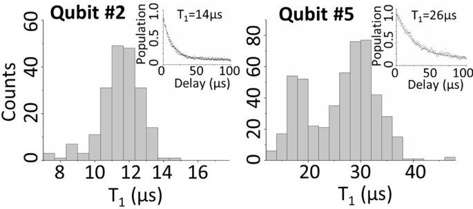
The histogram for qubit #5 appears bimodal, likely due to the intermittent interaction of the qubit with two-level systems. The insets show example T1 traces along with exponential fits. Each T1 measurement takes approximately 2 minutes and the total measurement time for qubits #2 and #5 was 8 hours and 20 hours respectively.
Purcell time was estimated using the approximation TPurcell ≈ Δ2/(g2κ), where κ is the spectral linewidth of the readout resonator. Referring again to Table 1, the measured T1 values are quite close to, and in some cases even exceed the estimated Purcell limit. This discrepancy is not necessarily nonphysical, as the Purcell rate estimation used here relies on a simplified model that does not include the experimental S21 background, modeled admittance of the resonator, and neglects the effects of higher-order resonances in the readout. Including higher-order resonances when modeling spontaneous emission has been shown to increase calculated Purcell times when qubits are detuned to frequencies below the readout, as is the case for the measurements presented here44. While the Purcell estimation raises the question of whether the T1 measurements provide an accurate assessment of device performance, it does establish a lower bound on the intrinsic quality factor of the Si-fin transmons, which may be reassessed with new devices following trivial modifications to the readout resonator to increase the Purcell time.
In conclusion, a fabrication process where parallel-plate capacitors are constructed from low-loss Si substrates has been evaluated for superconducting quantum computing applications. The Si-fin capacitors were incorporated in both lumped element resonators and transmons using established fabrication techniques. RF measurements of the resonators and transmons were performed at 35 mK and show that the devices are high performing: meeting or exceeding the state-of-the-art for comparable devices made using parallel-plate capacitors, with low-power Qi of the best lumped-element resonators exceeding 700k and the best transmon quality factors exceeding 750 k.
The computed Purcell time of the transmons was comparable and in some cases even greater than measured T1 times, suggesting the intrinsic quality factor of these transmons is likely higher. Moreover, the presence of stray capacitance in the LE design suggest that the intrinsic quality factor of these resonators may be higher as well, which implies that the figures of merit for the devices presented here should be taken as a lower bound. The Si-fin geometry allows for convenient and accurate capacitor definition as the capacitance is determined by the metallized length along the fins which is set using optical lithography in a subtractive process. The process presented may be used for applications that require a scalable process for compact, low-loss capacitors.
Responses