Magnetoelectric effect in van der Waals magnets

Introduction
The magnetoelectric (ME) effect was discovered a century ago and entered a renaissance with the advent of multiferroic materials1. ME effect manifests as the electrical control of magnetic polarisations or, reversely, the magnetic regulation of electrical polarisations. Such a feature intrinsically reflects the coupling of spin and charge degrees of freedom or more. As such, the ME effect is significant in both the fundamental physics of correlation and device applications, including magnetic sensors, logic and spintronic devices, and tunable microwave filters.
Before going straight into the ME effect found in vdW magnets, it would benefit the public if we discuss the more traditional multiferroic physics often discussed in the context of 3D magnets. A more usual definition of multiferroic is based on the linear ME effect that couples two otherwise independent degrees of freedom, spin and charge. This coupling, in principle, allows the control of charge by spin or vice versa, of which potential applications have been the source of much enthusiasm in the field. A dominant mechanism behind this interesting physics is the spin current model, where a noncollinear spiral magnetic structure produces an electric dipole via inverse Dzyalloshin-Moriya interaction2. Another equally viable mechanism is through a spin-lattice or magnon-phonon coupling3. Another noteworthy point about the 3D multiferroic materials is the classification. Two popular schemes are used: type I/II multiferroic and proper/improper multiferroic. The many multiferroic compounds can be divided into two groups4: type I multiferroics, where the ferroelectricity and magnetism occur at different temperatures and with different mechanisms, and type II multiferroics, where a magnetic order causes ferroelectricity.
Unlike these 3D multiferroic materials5,6, recent two-dimensional (2D) van-der-Waals (vdW) magnets7,8,9,10,11 pose the new potential to develop a more colourful landscape of the old-yet-classical ME effect and inspire many new opportunities in designing/manifesting/utilizing the ME effect from diverse angles of view. Most importantly, its intrinsic two-dimensionality offers a unique possibility that would otherwise be difficult, if not impossible, using bulk materials. In this review, we deliberately take a much broader view of ME effects than typically adopted in discussing 3D multiferroic materials. The benefit of adopting this broader approach is that it will allow us to cover more diverse and novel phenomena. This way, we can highlight some fascinating opportunities with the spin-charge coupling in 2D vdW magnets.
For example, NiI2 has been discovered as the first vdW multiferroic stable to very thin layers with a second harmonic generation response maintaining in a free-standing bilayer12 and even an hBN substrate-supported monolayer13. The ME physics of vdW magnets can be extended to other richer quantum effects such as quantum entangled magnetic exciton14. Another manifestation of the ME effect resides in NiPS3, where NiPS3 hosts an XXZ-type antiferromagnetic spin texture and, most importantly, a unique sharp magnetic exciton from the Zhang-Rice singlet to triplet transition15. A careful examination reveals that a small charge transfer occurs driven by a hybrid spin transition and a spin-orbit entanglement, eventually leading to an electrical dipole polarisation of roughly 0.1 ~ 0.2 µC/cm2 per NiS6 octahedron and consequent magnetic exciton15. This atomic ME effect is the origin of the strong spin-charge coupling, as reported earlier16, demonstrating a unique case of how the ME effect can arise from new quantum many-body phenomena.
Another interesting aspect of the ME effect in vdW magnets is its potential application in spintronics. For example, a novel atomic ME effect also exists in a ferromagnetic metal, e.g., the topological vdW perpendicular ferromagnet Fe3GeTe217. The atomic ME coefficient was theoretically investigated in terms of its symmetry and Berry curvature of the topological bands with spin-orbit coupling17. Surprisingly, such ME effect can be reflected in its free energy formula and greatly modify the spin-related free energy landscape, significantly lowering the switching barrier and reducing the switching coercive field correspondingly17. The large Berry curvatures lead to a gigantic intrinsic spin-orbit torque (SOT)17,18,19 by current in Fe3GeTe2 itself, reaching around 50 Oe/(mA/μm2)17. Such SOT value is about 100 times larger than conventional ferromagnet/heavy-metal composite systems, guaranteeing a highly efficient nonvolatile switching by current in its magnetic memory devices20,21. This Fe3GeTe2 case forms another case of bridging the underlying ME effect to fascinating quantum/topological properties and advanced spintronic applications.
These above scientific cases directly manifest the intrinsic ME effect at the atomic scale. More generally, the ME effect relates to any electrical manipulation of magnetic properties and vice versa. There are many interesting examples in the vdW magnet field; the most prototypical one is solid/ionic gating22,23,24,25,26,27. Gating can induce more electron or hole carriers in the system, shifting the Fermi level, altering the correlations and mediating the magnetic interactions in many vdW magnets22,23,24,25,26. In addition, constructing vdW hetero- or homo-structures based on vdW magnets can be another effective way to engineer the ME effect28,29,30.
This review aims to introduce these scientific examples and discuss these results in the context of the ME effect in vdW magnets. In this way, we want to emphasize the new insights and opportunities that 2D vdW magnets bring to advance and enrich the ME effect with a fresh viewpoint. Moreover, we provide more outlooks and a few examples of the ME effect’s revolution using quantum combinations and designs of vdW magnets. At the same time, we want to bring attention to several new concepts like quantum, topology, correlation, symmetry, etc., to leverage the atomic ME couplings.
Atomically thin multiferroic NiI2
Multiferroic materials show a coexistence of magnetic and ferroelectric order. The multiferroic systems provide an efficient route for controlling magnetism through an electric field and vice versa. Controlling magnetic order via an external electric field consumes less energy and complexity than controlling via a magnetic field. The vdW magnetic systems develop new paradigms for high-density magnetic memory due to their tiny volume and effective control of the magnetic state using external stimuli. Therefore, exploiting the vdW multiferroic material will provide promising candidates for future high-density, eco-friendly memory devices.
It is noteworthy that several halogenated compounds such as NiI2, CoI2, MnI2, and NiBr2 exhibit multiferrocity in the bulk crystals31,32,33. The multiferroic order of NiI2 persists down to the bilayer12 and even the two-dimensional limit at the specific condition13,34 in experiments. Bulk NiI2 has two successive magnetic phase transitions: the paramagnetic-to-antiferromagnetic transition at TN1 = 76 K and the helimagnetic transition at TN2 = 59.5 K (Fig. 1a). At the helimagnetic state, it develops a proper-screw spin helix with propagation vector Q = (0.138,0,1.457) in reciprocal lattice units. In such a noncollinear structure, the inverse Dzyaloshinskii-Moriya (DM) interaction or the spin-dependent metal-ligand hybridization induces nonzero electric polarisation. The induced electric polarisation is perpendicular to the magnetic propagation vector Q, developing in-plane ferroelectricity with six possible ferroelectric domains.

a Magnetic susceptibility of NiI2 with two successive phase transitions: the paramagnetic-to-antiferromagnetic transition at TN1 = 76 K and the helimagnetic transition at TN2 = 59.5 K. b In-plane ferroelectricity (P) with helimagnetic spin order. (Fig. 1a is reproduced from Fig. 1e in Ref. 14; Fig. 1b is reproduced from Fig. 1b in Ref. 12).
The optical second harmonic generation (SHG) measurements reveal its multiferroicity from the broken inversion symmetry in bulk and few-layer NiI2. The broken centrosymmetry from the electric dipole contribution gives rise to the nonzero SHG signal. The intermediate antiferromagnetic phase shows a small six-fold anisotropy pattern reflecting the triangular lattice symmetry. On the other hand, the multiferroic phase represents a two-fold symmetry with an enhanced SHG signal. Such an enhanced SHG corresponds to the ferroelectric order parameter, considering that SHG intensity is proportional to the square of electric polarisation. The multiferroic phase transition temperature also shows a strong thickness dependence. Figure 2 shows that the transition temperature decreases as the layer number decreases. The SHG signal persists down to the bi-layer and disappears in the monolayer. Another group also demonstrated the thickness-dependent multiferroicity in few-layer NiI2 on an hBN substrate grown by physical vapour deposition (PVD)13. The birefringence and SHG signals from the ferroelectricity are consistent with the previous results down to the bilayer: decreasing transition temperature with reduced thickness. In this case, the multiferroicity survives down to the monolayer. The discrepancy between the two studies on single-layer NiI2 from different sample preparations could be attributed to the strain effect from the substrate35. The following STM study also shows that single-layer NiI2 on top of highly oriented pyrolytic graphite (HOPG) provides additional proof of the two-dimensional multiferroicity34.
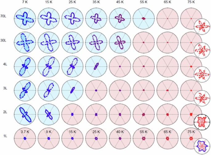
It shows different rotational anisotropy of the second-harmonic generation (SHG) pattern as a function of NiI2 thickness from 70 layers (70 L) to monolayer (1 L). Red and blue background colours highlight the transition to the polar state upon decreasing temperature. The red colour represents the non-ferroelectric state with a minute SHG response of six petals. In comparison, the blue colour represents the ferroelectric state with a significant SHG response of four petals. The ferroelectric state is maintained by an exfoliated NiI2 bilayer on the SiO2/Si substrate. (Fig. 2 is remade from Fig. 3 in Ref. 12).
The multiferroic state further induces magnetic exciton in NiI214. Optical absorption spectra reveal an exciton peak at 1.384 eV and a two-magnon sideband peak at 1.396 eV (Fig. 3). The exciton peak appears only below TN2, implying a connection to the multiferroic phase. NiI2 forms multiferroic domains in six directions, and these possible domains determine the angular dependence of exciton. Such an angular dependency of the exciton at 1.384 eV provides strong evidence of its association with the ferroelectric spiral phase. Combined with X-ray absorption spectra (XAS) and the resonant inelastic X-ray spectroscopy (RIXS), the mechanism of creation of magnetic excitons was studied. The magnetic excitons are generated from the Zhang-Rice triplet (ZRT) to the singlet (ZRS) transition. XAS reveals a relatively small charge-transfer energy of 1.498 eV, slightly larger than NiPS3 of 0.95 eV15 but significantly smaller than NiO of 4.6 eV36. Such a small charge-transfer energy is a prerequisite for the ZRT state. The RIXS and configuration interaction (CI) model will validate the ZRT to ZRS transition scenario in NiI2.
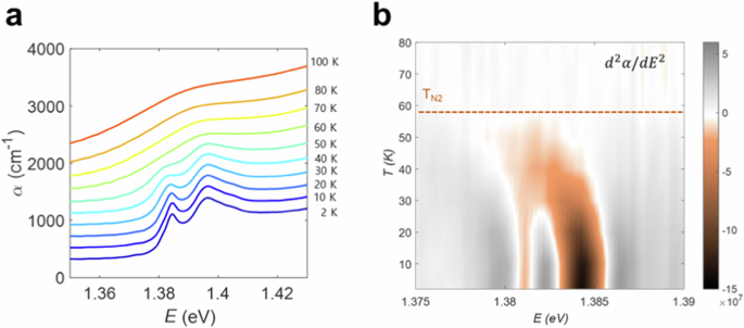
a Optical absorption of NiI2 with magnetic exciton at Ehv = 1.384 eV and two-magnon side-band peak at Ehv = 1.396 eV below TN2. b Derivative optical absorption shows a clear correlation between multiferroicity and the magnetic exciton. (Fig. 3a, b is reproduced from Fig. 2a, c in Ref. 14).
On the other hand, THz spectroscopy on NiI2 reveals two electromagnon modes at 34 and 37 cm−1 in the multiferroic phase at 2.5 K37. These energies are consistent with the energy scale of the two-magnon sideband excitation around the magnetic exciton peak. The reflection mode shows that these magnons are electric dipole active rather than magnetic dipole active. The observed electromagnon mode shines a valuable light on the origin of the very strong magnetoelectric coupling in NiI238. The following study employs time-resolved optical SHG and Kerr rotation microscopy to reveal the nature of the electromagnons. SHG is sensitive to the electric dipole polarisation, and Kerr rotation microscopy is sensitive to the magnetic order; therefore, analysing these two results gives a comprehensive understanding of the electric polarisation and magnetization components. Perturbing the multiferroic state with a laser pulse triggers coherent oscillations of the electromagnon modes. Two time-resolved optical techniques, SHG and Kerr rotation, show the emergence of an π/2 phase shift between the electric polarisation and magnetization oscillations. The estimated dynamical magnetoelectric coupling strength surpasses other multiferroics, such as CuO39. Such a substantial enhancement originates from the synergy between the noncollinear spin texture and spin-orbit interaction on the ligands and d-p hybridization compared to the phonon-mediated electromagnons.
As mentioned previously, several other vdW multiferroic systems exist besides NiI2. Future systematic studies will be helpful in most of these systems, such as the thickness dependence of multiferroicity as performed in NiI2. It is encouraging that theoretical studies predicted that some metal halides could host multiferroicity even in the monolayer limit40,41. To experimentally realize multiferroicity in monolayer or few-layer metal halides, however, there are some realistic experimental challenges to overcome, at least including issues like a proper substrate for stabilizing multiferroic states and encapsulation for preventing degradations due to their air-sensitivity. Another interesting vdW multiferroic material, CuCrP2S6 was also studied using multiple probes such as magnetization, electrical transport, and SHG measurements, expanding the vdW multiferroic investigations42,43. Further exploiting the vdW multiferroic materials will stimulate new methodologies for controlling the multiferroicity in the atomic layer limit.
Atomic magnetoelectric effect in NiPS3
NiPS3 is a charge transfer (CT) insulator that exhibits zigzag antiferromagnetic ordering16,44,45. Previous studies have estimated the CT energy to be either negative16 or within a small positive range from 0.9 to 2.5 eV15,46,47. The small CT energy, combined with strong pd–σ hybridization, causes doubly degenerate unoccupied Ni eg orbitals to mix with occupied ligand p orbitals from the surrounding six sulphur atoms. This leads to the spontaneous population of self-doped ligand holes48. The combination of a hole at the Ni site and a self-doped ligand hole forms spin-orbital entangled many-body states within the NiS6 octahedron, manifesting as spin-triplet and orbital singlet states15,47,49,50. These CT states are reminiscent of the Zhang-Rice triplet (ZRT) states observed in high-TC cuprates51,52. Recent studies suggest that the ground state of NiPS3 is a mixture of approximately 60% triplet states from the d8 configuration and about 40% ZRT states from the d9L1 configuration, where L represents the ligand hole15,47.
In this context, we examine the self-doped ligand distribution of the ZRT states within the honeycomb lattice. When ZRT states form in each NiS6 octahedron, two types of orthonormal S 3p holes can populate the sulphur sites, forming spin-triplet states with neighbouring Ni 3 d orbitals. Under zigzag magnetic ordering, two edge-shared sulphur sites emerge based on the spin configurations of neighbouring Ni ions: S1 sites with parallel spin alignments and S2 sites with anti-parallel spin alignments. At S1 sites, the two-hole orbitals share the same spin, whereas they have opposite spins at S2 sites (see Fig. 4a). Charge disproportionation between these two sulphur sites induces charge-stripe modulation, which can lead to local electronic dipole polarisation. Many-body calculations have shown that exchange correlations (Hund’s coupling) between self-doped holes can cause charge deviations of approximately 0.002 ~ 0.003|e| between the S1 and S2 sites, as shown in Fig. 4c, resulting in a local dipole polarisation of around 0.1 ~ 0.2 µC/cm2 per NiS6 octahedron15. Alternatively, atomic spin-orbital coupling, combined with non-cubic hopping and spin-orbit coupling, has generated a local dipole polarisation of about 10-5 µC/cm2 in the ZRT state under zigzag magnetic ordering50. These induced local electronic dipoles give rise to the atomic magnetoelectric effect.
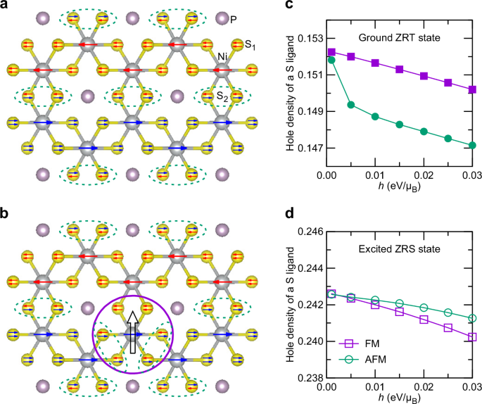
a, b Schematic diagrams of spin configurations in a the Zhang-Rice triplet (ZRT) lattice and b the Zhang-Rice singlet (ZRS) excited lattice under zigzag magnetic order in NiPS3. Large (small) red and blue arrows represent the spin directions of Ni 3 d (S 3p) holes, respectively. Green dotted ellipsoids highlight S2 sites, where two ligand holes exhibit anti-parallel spins, while S1 sites, where the two holes have parallel spins, are depicted for the other S atoms. The magenta circle indicates the locations of ZRS excitations. Due to spin flipping in one of the hole orbitals at the surrounding S sites, the transition from ZRT to ZRS states leads to polarisation reversal. It induces electric dipoles, with the direction indicated by the open arrow inside the magenta circle. c, d Hole density of an S ligand as a function of the long-range ordering field strength h, for the ground ZRT state c and the excited ZRS state d, respectively, as calculated in a Ni2S10 cluster (see details in Ref. 15). FM (AFM) refers to cases where the applied long-range ordering fields at the two Ni sites are parallel (anti-parallel). The differences in hole density between the FM and AFM cases in c and d indicate the charge modulations of self-doped ligand holes at S1 and S2 sites in the ground ZRT state and the polarisation reversal in the excited ZRS state, respectively. (Fig. 4 is remade from Fig. S9 in Ref. 15).
The atomic magnetoelectric effect contributes to the spin-charge coupling observed in optical excitations16,53,54. A prominent manifestation of this effect is the magneto-exciton behaviour in an ultra-narrow exciton peak at around 1.476 eV15,55,56,57,58,59,60. This exciton becomes optically bright only when the zigzag magnetic order is stabilized and exhibits two-fold intensity anisotropy under an in-plane magnetic field. The magneto-exciton behaviour can be explained by the emergent electric field induced by the reversal of local dipole polarisation during the transition from the ground ZRT state to the excited Zhang-Rice singlet state (see Fig. 4b, d). Additionally, these excitons show anisotropic Zeeman-like splitting in resonance with an in-plane magnetic field61,62,63. This splitting can also be interpreted as a magnetic exciton arising from singlet-triplet transitions62,63. Consequently, the atomic magnetoelectric effect in NiPS3 can present potential applications for optical spin read-out devices and two-dimensional opto-spintronic technologies56,62. The intriguing ME effect in NiPS3’s quantum-entangled many-body magnetic exciton will also motivate a more detailed examination of other magnetic exciton or spin-orbit exciton systems, such as layered RuCl364. In addition, the electronic and magnetic structure may also be strongly intertwined in similar family systems like FePS365, etc.
Current-induced magnetoelectric effect and spin-orbit torque in Fe3GeTe2
Charge current can generate spin polarisation and so imbalance due to spin-orbit coupling with the mechanisms of spin Hall effect or interfacial Edelstein effect. Such spin polarisation can exert a torque onto the magnetization, called spin-orbit torque (SOT), which conventionally occurs in a ferromagnet/heavy-metal bilayer and depends on the symmetry of the system66,67. Fe3GeTe2 represents the earliest discovered vdW ferromagnetic metal with a high Curie temperature of ~200 K and a perpendicular magnetic anisotropy68,69, and thus has been widely studied for spintronics, particularly the SOT. Conventional protocol of SOT has been applied in a Fe3GeTe2/Pt system70,71. At the same time, a different type of gigantic intrinsic SOT17 in Fe3GeTe2 itself has also been established in recent years. The following paragraphs discuss such gigantic intrinsic SOT by current and the underlying atomic ME effect related to band topology.
Monolayer Fe3GeTe2 has three unique symmetries, including C3, mz and my. A theoretical work18 examined its SOT and found that all the SOT coefficients will be cancelled out regarding symmetry except for a constant Γ0. This SOT term can be turned into its free energy formula. Another theory and experiment combined work17 develops at the same period. The theory found that the SOT term can change the spin-related free energy landscape and reduce the perpendicular magnetic anisotropy by lowering the switching barrier for spin up-to-down transition. In addition, they started from the Kubo formula and derived a formula for calculating the SOT strength. Note that this derivation process handles a question of how much spin accumulation is produced per current, reflecting the microscopic ME effect. The calculated SOT strength, or in the language of the ME effect: the atomic ME coefficient (Γ0) is surprisingly found to be as large as ~30 Oe/(mA/μm2). The derived ME formula highlights the effective spin accumulation or the Berry curvature accumulation per current in this system17. Therefore, the obtained large ME coefficient17 is consistent with the previously reported large Berry curvature of FGT’s topological bands72,73. In the experiment (Fig. 5a–c), a giant coercivity reduction by the current was discovered after subtracting off the Joule heating’s contribution using three different but consistent methods. Such substantial coercivity reduction directly results from SOT-reduced magnetic anisotropy and switching energy barrier, ultimately reflecting the strong atomic ME effect. They estimated the atomic ME coefficient from coercivity reduction to be 50 Oe/(mA/μm2), which is close to the theoretical calculation. The ME-related SOT scenario was coherently supported by three approaches: coercivity reduction, theoretical calculations and in-plane angular magnetoresistance. This bulky SOT in Fe3GeTe2 has also been confirmed by another work from an independent group using the second harmonic technique for electrical transport74.

a Increasing current induced substantial reduction of coercive field. b Large coercivity reduction after Joule heating’s contribution subtracted off. c Spin-orbit torque (SOT) magnitude extracted from coercivity reduction for devices of varying thickness. The net SOT magnitude (blue points) shows no noticeable thickness dependence, with device thickness ranging from 6 to 40 nm. d SHG schematic on bulk Fe2.8GeTe2. e, f SHG response for the PP mode e shows a prominent three-fold petal, while for the SS mode f is nearly zero. It shows that inversion symmetry has been broken, mainly along the out-of-plane direction. g Comparison of SOT magnitude of different systems, where the ME/SOT coefficient is about 100 times larger than that of conventional heavy metals. h A novel type of magnetic memory has been demonstrated based on the gigantic intrinsic SOT. The switching current density and power dissipation are around 400 and 4000 times reduced compared to the conventional Pt/Co devices. i Eight multi-level states controlled nonvolatilely by tiny currents, corresponding to 3 bits in a single-device magnetic memory. (Fig. 5a–c is reproduced from Fig. 2a, Fig. S4f, and Fig. 3e respectively in Ref. 17; Fig. 5d–f is reproduced from Fig. 1a–c in Ref. 19; Fig. 5g is reproduced from Fig. 3f in Ref. 17, and Fig. 5h, i is reproduced from Fig. 3d and Fig. 5c respectively in ref. 20).
Surprisingly, the SOT coefficient is about 100 times larger than that of conventional heavy metals like Pt and Ta17, demonstrating a strong ME effect that a tiny current can produce a sufficiently large magnetic polarisation. Meanwhile, such SOT occurs in a ferromagnet Fe3GeTe2 without any heavy-metal layer and is deeply rooted in its band topology and Berry curvature17. Unlike normal metals or Weyl semimetals75,76, Fe3GeTe2 has a topological Nodal-line band structure and consequent large Berry curvature72, and thus eventually large ME effect and SOT magnitude17. One interesting question from this work17 is how to explore a new larger SOT system with band topology. For instance, the larger ME and SOT effect requires large spin polarisation by current due to large spin-orbit coupling or spin Hall effect or the Edelstein effect. These effects require large Berry curvature intrinsically in a material system from the viewpoint of theoretical calculations of Nodal-line materials. Following this logic, one would see huge opportunities to explore the gigantic ME effect in topological Nodal-line materials.
Another insight can be obtained from the symmetry perspective. Since the ME and the SOT coefficients shall conform to the crystalline symmetries, one can explore similar systems containing the same symmetries. Their SOT term will also be simplified in the same way under those symmetries to be incorporated in its free energy expression, enabling the reduction of magnetic anisotropy. Indeed, three reports77,78,79 followed the previous pioneering work17, and used another same-structure material, Fe3GaTe2, to reproduce all the physics and magnetic memory applications of Fe3GeTe2 but at room temperature. We expect more exciting similar systems regarding symmetry in the future, hosting the same ME and SOT physics.
A final issue in this fundamental ME and SOT physics is the inversion symmetry breaking: bulk Fe3GeTe2 is long thought of as centrosymmetric with layer inversion, but SOT requires inversion symmetry breaking. Previous work17 addressed this symmetry problem by considering a hidden SOT effect in analogy to the hidden Rashba effect in centrosymmetric systems80. Specifically for Fe3GeTe2, the intralayer magnetic interaction is ~1 eV, about three orders of magnitude higher than the interlayer interaction of ~1 meV and predominates the SOT without considering interlayer interference. Although it nicely explained the symmetry contradiction, it didn’t exclude another possibility that inversion symmetry can somehow be broken in actual Fe3GeTe2 materials. Very recently, the same group discovered the defect-related inversion symmetry breaking by the SHG technique19, adding another contribution to the intrinsic SOT in bulk Fe3GeTe2 (Fig. 5d–f). They found that Fe vacancy imbalance can break inversion symmetry mainly along the out-of-plane direction, reducing the space group from centrosymmetric P63/mmc to noncentrosymmetric P3m1, consistent with a related structural investigation81. The SHG response evolves from a three-fold petal to a more isotropic pattern as the Fe ratio increases from 2.8 to 3, highlighting the defect-breaking layer inversion in bulk Fe3GeTe2 single crystals.
Meanwhile, the SHG response is independent of temperature and thus purely coming from structural variations. Note that such inversion symmetry breaking is weak, however general it is in similar systems of layer inversion. Moreover, it may affect band topology and other symmetry-related quantum characteristics and hints at other inversion-symmetry-breaking-required phenomena, such as nonlinear optical and electrical response, nonreciprocal transport, and diode effect. Fe3GeTe2 can also be regarded as the first topological vdW ferromagnetic polar metal ever discovered.
All the above discussions paint a complete physical picture of the atomic ME and intrinsic SOT effect in a single Fe3GeTe2. These ingredients enable highly efficient magnetic memory with processed developments. In 2021, a novel type of conceptual magnetic memory device20 has been proposed and systematically demonstrated based on this principle (Fig. 5g-i). The magnetization switching by current is highly efficient and also nonvolatile: the switching current density and power dissipation were reduced by 400 and 4000 times compared to conventional Pt-based devices20. Moreover, multi-level states have been readily controlled by tiny current nonvolatilely in the device, which shows around eight states corresponding to 3 bits in a single device, thus enhancing the single-device information capacity and reducing computing cost20. Inspired by these two SOT works17,20, another group succeeded in the real-space imaging of the above switching process by current and the measurement of the domain motion velocity82. In 2024, three different works reproduced the same physics and spin memory chip devices using the same-family material Fe3GaTe277,78,79 at room temperature. Finally, the same group initializing these intrinsic ideas realized the all-vdW three-terminal SOT-MRAM device, where the SOT-writing and TMR-reading process are physically separated to naturally enhance the design flexibility and device endurance, which is closest to an industrial SOT-MRAM architecture. With their fascinating ME and SOT physics and abundant device application demonstrations, the vdW magnets are expected to expand the ME effect towards more exciting spintronic applications.
Electrical gating on vdW magnets and magnetic control of their electronic properties
In a broad sense, the ME effect can be defined as any electrical control of magnetic properties and, reversely, the magnetic control of electrical properties. Under this context, the most outstanding ME scientific case is the electrical gating of vdW magnets benefiting from its 2D materials’ nature. In light of vdW magnetic insulators, CrI3 (Fig. 6a, b) and CrGeTe3 (Fig. 6c, d) are most popular in this aspect. For example, monolayer CrI3 is an Ising-type ferromagnet whose magnetization can be changed by a solid gating voltage22. Bilayer CrI3 is an A-type antiferromagnet with an out-of-plane easy axis, where the spins are aligned parallel intralayer for each layer, but anti-parallel interlayer22,23. Solid gating a bilayer CrI3 can modulate its magnetization and even realize the antiferromagnetic to ferromagnetic transition under a finite or zero magnetic field22,23. The saturated magnetization of CrGeTe3 was also prominently changed in a gating experiment24. Moreover, a bipolar tunable magnetization was reported and ascribed to the moment rebalance in the spin-polarised band structures of CrGeTe324.
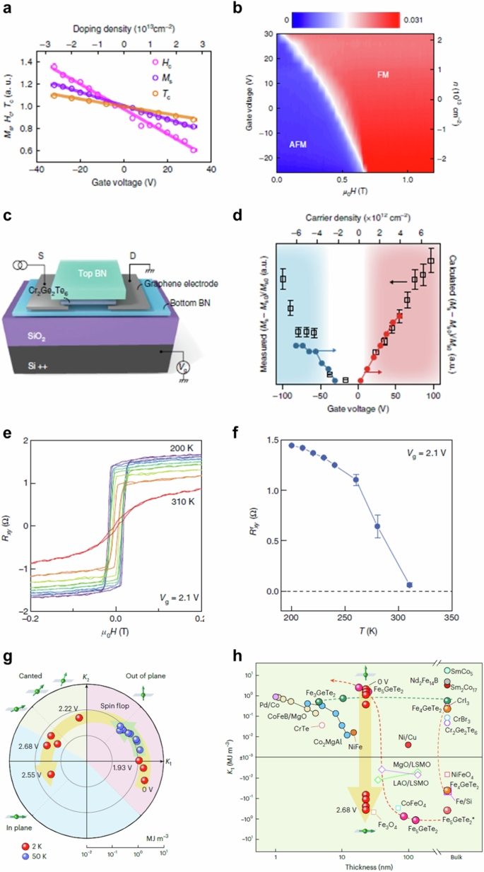
a Monolayer CrI3’s saturated magnetization, coercivity, and Curie temperature can be linearly reduced by increasing gate voltage. b Gating a bilayer CrI3 leads to a antiferromagnetic to ferromagnetic transition. c Back gate schematic for CrGeTe3 nanoflakes. d CrGeTe3’s saturated magnetization can be enhanced by both positive and negative gate voltages. e, f Ionic gating on a four-layer Fe3GeTe2, where the Curie temperature was boosted to 310 K at a gate voltage of 2.1 V. g, h Ionic gating on a Fe5GeTe2 nanoflake tune the magnetic anisotropy from an out-of-plane to in-plane easy axis continuously. The K1’s magnitude changes widely across a five-order range. (Fig. 6a, b is reproduced from Fig. 2c and Fig. 3b respectively in Ref. 22; Fig. 6c, d is reproduced from Fig. 3a and Fig. 5d respectively in Ref. 24; Fig. 6e, f is reproduced from Fig. 4a, b in Ref. 25; Fig. 6g, h is reproduced from Fig. 4a, b in ref. 26).
For vdW magnetic metals, ionic gating is much more efficient than solid gating, as reported in many works. For a typical ferromagnetic metal Fe3GeTe2 (Fig. 6e, f), one group developed the Al2O3-assisted technique to exfoliate few-layer and monolayer Fe3GeTe2. It measured their anomalous Hall effect when applying ionic gating down to monolayer25. The magnetization and coercive field have been greatly modulated during the electrical gating. Most strikingly, for a four-layer Fe3GeTe2, the Curie temperature has been enhanced to ~310 K, much larger than even the bulky Curie temperature of ~205 K in bulk Fe3GeTe2. For another near-room-temperature ferromagnetic metal Fe5GeTe2 (Fig. 6g, h), ionic gating can even continuously tune its magnetic anisotropy and demonstrate a gradual transition of an out-of-plane easy axis to an in-plane one26. It is noted that both carrier doping and electric field can affect magnetism, each of which may be dominant for different experiments. Therefore, careful designs and delicate experiments should be performed regarding this fundamental issue. For instance, the carrier doping effect dominates in some cases, such as in the Refs. 22,23,25,26, while the electric field effect plays significant roles in several other cases24,83. These four cases are interesting enough to reveal the electrical gating modulation of magnetic properties in vdW magnets, where the saturated magnetization, coercive field, magnetic anisotropy and even the magnetic ground states can be substantially modified by varying the gating voltages. These experiments leverage the charge density variation, electric field effect, Fermi level shift, correlation modification and ultimately magnetic interaction alteration to manipulate the magnetic properties, showcasing the hugely interesting ME effect by electrical means for vdW magnets.
On the other hand, magnetic control of electronic properties has also been reported in several cases with vdW magnets. For example, in bilayer CrSBr, an external magnetic field can induce the exciton energy shift and intensity change due to the spin-flip or spin-canting driven spin configuration change84. Theoretically, when spin order changes from antiferromagnetic (AFM) to ferromagnetic (FM) configuration, the interlayer hybridization enhances and leads to the conduction-band-minimum (CBM) and valence-band-maximum (VBM) splitting and consequent band gap reduction. Meanwhile, interlayer hybridization makes relaxation into the lowest-energy bright exciton more efficient and thus makes the PL process more competitive compared to the non-radiative recombination, leading to the PL intensity increase for the FM states. In addition, CrX3 (X = I, Br) is another representative material in which exciton couples with magnetic ordering85,86. In this system, PL intensity changes upon applying an external magnetic field, depending on the handedness of the incident and detected light. Such spin-selectable signals can be confirmed not only through emissions but also via current intensity measurements, for instance, using the photovoltaic effect87. In particular, CrI3 is a vdW A-type antiferromagnet and thus allows the controllability of its magnetic hysteresis curve depending on whether the layer number is even or odd. Similarly, MnBi2Te4 features either an axion insulator or a Chern insulator depending on its spin order88, providing another example of the topological ME effect.
Outlook to ME effects in vdW quantum magnetic hetero- or homo-structures
Another promising strategy for producing the ME effect is constructing vdW heterostructures by stacking ferromagnetic and ferroelectric materials. In these heterostructures, the broken inversion symmetry at the interface of the two layers can induce a significant ME effect, even if neither material individually exhibits such behaviour. This phenomenon emerges due to the coupling between the ferroelectric polarisation and the magnetic moments at the interface. For example, in the Fe₃GeTe₂/In₂Se₃ heterostructure, it has been experimentally demonstrated that applying a voltage can control the magnetic properties of Fe₃GeTe₂ through the interface coupling with In₂Se₃, thus enabling an electrically tunable ME effect30. Two other equally important works include the ferroelectric/ferromagnet heterostructures of Cr2Ge2Te6/P(VDF-TrFE)89 and Fe3GaTe2/CuInP2S690, where a voltage applied to the ferroelectric can control the 2D magnetism in cryogenic and room temperature, respectively. Similarly, in other heterostructures, the coupling between ferroelectricity and magnetism has shown potential for nonvolatile memory devices, where electric fields can control magnetic states28,29. When designing vdW bilayer structures for the ME effect, lattice mismatch is so critical that a large mismatch can weaken interlayer coupling. One solution to this problem is to create homostructures. A well-known phenomenon related to this is broken inversion symmetry induced by the sliding effect in MoS₂ homostructures, which creates a small dipole moment. In this structure, the lattice reconstruction has revealed polarisation in two anti-parallel directions. It is experimentally achieved by stacking layers at specific angles, resulting in a polarisation along the c-axis, which can be controlled electrically91,92.
Similarly, for magnetic vdW materials, stacking engineering can break inversion symmetry even in non-polar structures, thereby inducing a ferroelectric state. In such cases, the interaction between ferroelectric and magnetic ordering can be activated, offering the potential for multiferroic properties. This stacking-engineered ME effect can be applied to study strong intrinsic spin fluctuations associated with two-dimensional magnetism while overcoming material limitations like lattice mismatch. One example is to use this structure as a platform for electrically tuning magnetic domains. This enables the observation of magnetic domains and their boundaries, which is crucial in manifesting magnetic topological effects in various systems. Additionally, it aids in analysing changes in magnetic order due to variations in strain or stacking order, providing insights into ME behaviours at the nanoscale and furthering our understanding of the fundamental physics of two-dimensional magnets.
Summary
2D vdW magnets provide enormous opportunities for investigating the ME effect at macroscopic and atomic levels, including striking phenomena and underlying mechanisms. In this review, we summarise the ME effect in different vdW magnets, including multiferroic in NiI2, spin-charge correlation in NiPS3, atomic intrinsic SOT in Fe3GeTe2, gating controlled magnetism in CrI3, Cr2Ge2Te6, Fe3GeTe2, and Fe5GeTe2, reflecting diverse aspects of the ME effect’s manifestation. Finally, we also provide a promising outlook and a few cases on the ME effect in quantum hetero- or homo-structures enabled by assembling these 2D magnets, which can be an exciting new direction along this atomic ME effect topic and corresponding device applications.

Responses