Connecting physics to systems with modular spin-circuits

Introduction
The rise of Artificial Intelligence with its skyrocketing computing needs coincided with the stagnation of Moore’s Law. This clash has been driving the development of domain-specific hardware1 and architectures with a wide variety of heterogeneous systems for computing, memory, and sensing applications. In this new era, rapid and accurate tools for evaluating the potential of emerging materials, physical phenomena, and device concepts have become a crucial need. Such tools will have an impact not only in moving forward well-established computational schemes but also in opening new directions in unconventional computing paradigms2.
In this perspective, we describe a physics-based circuit approach that covers a wide range of phenomena in spintronics and magnetism using a generalized circuit theory. We show how circuit “modules” derived out of microscopic theory and phenomenological models can accurately model spin transport while accounting for magnetization dynamics.
Combining phenomenology and microscopic theory, the spin–circuit approach for spintronics has been used to model non-local spin–valves, channels with high-spin orbit coupling such as semiconductor channels with Rashba interactions, heavy metals and topological insulators, transport in ferromagnetic insulators, ferromagnet-normal metal interfaces, spin–pumping phenomena, magnetic tunnel junctions, voltage controlled magnetic anisotropy, finite temperature magnetization dynamics and others. A web page with open-source models along with open-source SPICE codes catalog these results3.
The key strength of the approach is not just about modeling phenomena, but more about its ability to combine the modules to design new circuits and structures. For example, given interface, bulk magnet, magnetization dynamics, and spin–orbit channel modules, complicated new devices can be constructed and studied (see, for example, refs. 4,5). Real-time simulation of nanomagnet dynamics coupled with transport modules allows accurate transient simulations from which device characteristics can be obtained. Powerful tools and analysis options of mature circuit simulators greatly ease a wide range of measurements for AC, DC, transient, and noise analysis. Our transport conductances are based on low-frequency (DC) analysis, but they can be dynamically controlled by changing magnetization vectors. We assume that these changes occur instantaneously, allowing the transport to be described using lumped circuit models.
Another distinguishing aspect of spin–circuits compared to powerful alternatives to model spintronic phenomena6,7 is how new devices and phenomena can be seamlessly integrated with state-of-the-art complementary metal oxide semiconductor (CMOS) transistor models. This combination allows fast, accurate, and informative evaluation of CMOS+ ({mathsf{X}}) platforms (where ({mathsf{X}}) can be any emerging CMOS-compatible technology such as spintronics, ferroelectrics, and photonics) using efficient circuit simulators (e.g., SPICE and its variants).
The spin–circuit approach evolved out of a 2-component model involving collinear spins8, which is relatively intuitive. It is as if there are two species of electrons, up and down. The charge current is the sum of up and down currents, while the spin current is given by their difference.
Less intuitive is the 4-component model with noncollinear components, 1 for charge and 3 for spin (see, for example9,10, and references therein). The 4-component model is not based on four species of electrons. Rather, it is based on two components with complex amplitudes {uv} that embody subtle quantum physics. For example, {10} represents +zspin, {01} represents −zspin, while a superposition of the two {11} represents +xspin. This can lead to quite non-intuitive results like a flux of +xspins getting converted into +zspins by a shunt path that pulls out −zspins11.
Even such non-intuitive effects are accurately captured by the 4-component model whose components represent measurable quantities given by bilinear products of u and v. For the 2-component wavefunction ψ = {uv}T with complex components:
where ρ is the density matrix at a given point in the real space representation. The charge and spin components are then given by ({rm{tr}}(rho {sigma }_{i})) where σi are Pauli spin matrices for x, y, z, and the identity matrix for charge. Then, the charge component is given by uu* + vv* while the three components of the spin are given by uu* − vv* (z-spin), 2Re(uv*) (y-spin) and −2Im(uv*) (x-spin).
The 4-component spin–circuit equations have later been converted into convenient and intuitive 4-component circuits where currents and voltages carry 3-spin and 1-charge components that are related by 4 × 4 conductances matrices. Many examples of spin–circuits to model existing and evaluate new device concepts have been performed over the years, by the authors and others12,13,14,15,16,17,18,19,20,21,22,23,24,25,26,27,28,29,30,31,32,33,34,35.
We first give a brief introduction to the spin–circuit approach discussing the basics of the transport and magnetism modules and how they interact. To illustrate how extensible and modular the approach is, we present several original examples of the approach by constructing new spin–circuits. Some of our examples are chosen in the context of a new and emerging computational paradigm with probabilistic bits, covering physics, devices, circuits, architectures, networks, reaching all the way up to the algorithms that run on this stack (Fig. 1). The ideas related to probabilistic computing came long after the spin–circuit approach but as we will show, spin–circuits have been instrumental in helping uncover new physics and new potential applications due to their modularity enabling a “plug and play” approach.

a Physics: Spin–circuits solve transport and magnetization dynamics self-consistently. b Devices: example stochastic MTJs (with spin–orbit and spin–transfer torque) using low-energy barrier magnets. c Circuits: stochastic neurons (p-bits) built out of stochastic MTJs. d Architectures: Probabilistic architectures with interacting stochastic neurons. e Networks: networks of p-bits mapped to computationally hard optimization problems. f Algorithms: powerful algorithms that use replicas of probabilistic networks to help solve these optimization problems.
Spin transport with 4-component circuits
The two main ingredients in the spin–circuit approach are transport and magnetism modules that need to be solved self-consistently. Transport timescales are typically much faster than magnetization dynamics and this allows a lumped circuit description of transport modules that are solved for each new magnetization configuration in the circuit. We first start by describing spin–transport modules.
Transport modules are naturally represented as circuits, but they need to be generalized to include spin transport. If a conductance (or resistance) based formulation for circuit theory is desired, the principled approach is to start from a quantum transport formulation to obtain related terminal currents to terminal voltages in terms of conductance matrices. These matrices are of dimension 4 × 4 in the case of spin transport relating 4-component current and voltage vectors, one component for charge and three components for spin directions (we show a concrete example in Section “Channels with spin–orbit coupling”).
The key point, however, is that a fully phase-coherent description of conductors is often unnecessary since spin conductors generally conserve spin information captured in the 2 × 2 Hermitian part of the density matrix at a real space point, but longer spatial correlations are often irrelevant and they need to be taken out by computationally expensive dephasing mechanisms. As we will show, the spin–circuit approach we discuss can combine diffusive spin conductances with coherent spin conductances, where the coherent part can often be restricted to a small “active” region of interest. This effective combination ensures that quantum transport is accounted for only when it is needed. We stress that our examples in this paper are exclusively on spin–transport, but extensions to the valley or more complicated degrees of freedom should be possible using similar approaches.
As we discuss next in Section “Two-port formulation of spinconductances”, the non-conservative nature of spin–currents necessitates care in a circuit description of spin conductances. These non-conservative currents are naturally handled by shunt conductances that are connected to grounds. The resulting circuits fully satisfy Kirchhoff’s laws and can be handled by powerful circuit simulators11,15,36. A microscopic formulation of a 4-component formulation of spin–currents was first explored in refs. 9,10, focusing on metallic and ferromagnetic channels. In our view, however, the spin–circuit formalism is much broader. Even though starting from microscopic theory may not always be necessary or possible, phenomenological 4-component spin–circuit models can still be obtained. Examples of these include spin–circuits for channels with spin–momentum locking37, such as heavy metals with giant spin Hall effect20, topological insulators20,23, magnonic transport magnetic insulators38, and others.
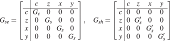
Two-port formulation of spin conductances
The 4-component conductance formulation is rooted in a 2-port description of transport. For a 2-terminal conductor, the two-port formulation relates currents to voltages. In ordinary charge conductors, the 2-port formulation simplifies due to Kirchhoff’s current law, which enforces current conservation: I1 + I2 = 0. This results in constraints like G11 = −G21 and G22 = −G12, and if reciprocity holds (G12 = G21 = G0), only one independent parameter, G0, is needed to fully describe the 2-port conductance matrix. This is why ordinary circuit theory typically does not use a 2-port formulation. For general conductances, neither reciprocity nor current conservation is guaranteed. In spin circuits, unlike charge currents, spin currents are not strictly conserved due to various relaxation processes, such as spin-flip scattering and spin dephasing, or due to coherent rotations from spin–orbit coupling and external magnetic fields. These mechanisms unbalance the spin currents entering and exiting ports, manifesting as G11 ≠ −G21 in the 2-port formulation. Nonetheless, it is still possible to represent the 2-port description in terms of a standard circuit with shunt conductances (Fig. 2). When the spin conductance is reciprocal (G12 = G21 = G0), the system can be represented with shunt conductances Gsh1 = G11 + G0 and Gsh2 = G22 + G0 at each terminal. These shunt conductances capture the losses from spin relaxation or coherent rotations, analogous to how shunt elements handle signal losses and dissipation in microwave circuits39. This reciprocal assumption simplifies the circuit representation, as it allows symmetric handling of currents at both ports. For non-reciprocal spin conductors, additional elements such as dependent sources may be required to capture the asymmetric nature of spin current flow40. We will examine an example of a non-reciprocal conductance in channels with spin–momentum locking in Section “Channels with spin–orbit coupling”. Modern circuit simulators like HSPICE can also take in the constitutive 2-port relations directly to describe conductances, so both of these representations may be useful.
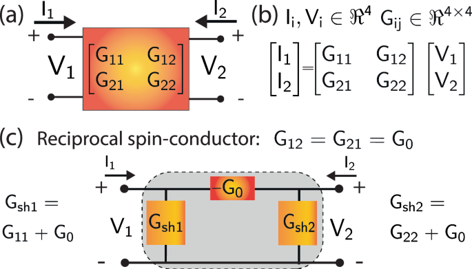
a Any 2-terminal spin conductor can be formulated in terms of 2-port conductance matrices between its terminals. b The currents and voltages are related to each other by 4 × 4 conductances Gij and currents and voltages are 4-component vectors. c Unlike charge currents, spin conductors may exhibit non-conservation of currents (I1 + I2 ≠ 0) and non-reciprocity (G12 ≠ G21). Here, we show an example of a reciprocal spin conductor (G12 = G21 = G0). Even with the conservative nature of spin currents, it is possible to obtain a circuit description by introducing shunt conductances from the terminal to the ground to account for losses through spin–relaxation or coherent rotation mechanisms.
The 2-port formalism is entirely general and agnostic to where the conductances Gij come from. The examples we consider in this paper cover widely different regimes from coherent quantum to semi-classical diffusive transport. The conductances can originate from microscopic, phenomenological theory or experiments.
Ferromagnet-normal metal interface
For many spintronic devices, a key component is the ferromagnet-normal metal interface (F∣∣N), where the spin–transfer-torque effect occurs. A four-component circuit formulation of the F∣∣N interface can be obtained from scattering theory or the non-equilibrium Green’s function formalism9,36,40. The F∣∣N interface consists of a series and a shunt component (Fig. 3a) that both depend on the orientation of the ferromagnet. When the ferromagnet points in the +z direction, these conductances are given by:
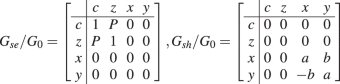
where G0 is the interface conductance, P is the interface polarization, a, b are the real and imaginary coefficients of the “spin-mixing conductance”, respectively. The form of these conductances is intuitive: the series conductance creates spin-polarized spin currents when subject to a charge potential, and shunt conductances are responsible for absorbing transverse spin currents that result in the spin–transfer–torque effect.
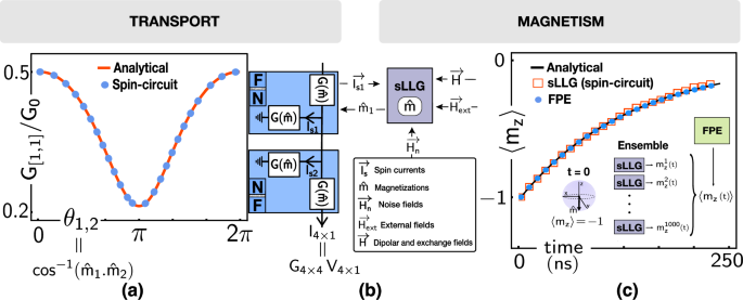
a An example spin–valve built out of two interfaces is shown. Numerical results obtained from spin–circuits are compared with theory9 where the charge conductance shows magnetoresistance as a function of the relative angle between the ferromagnets. b Spin–circuit model illustrating the interaction between the magnetization dynamics (modeled by sLLG) and transport modules. The transport model receives two magnetization vectors from the stochastic LLG and produces 4-component spin currents carrying charge and spin information. sLLG receives spin currents and magnetic fields and produces a magnetization vector. c sLLG results are benchmarked with the Fokker–Planck equation (FPE). One thousand low-barrier nanomagnets (with a very small perpendicular magnetic anisotropy) are prepared in the −1 direction and left to relax. The average magnetization (leftlangle {m}_{z}rightrangle) is measured over time and compared to FPE and the analytical solution (see text).
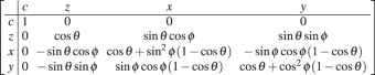
Naturally, in settings where transient behavior needs to be examined, conductances need to be modified in conjunction with moving ferromagnetic magnetization vectors. This can be carried out by a standard rotation matrix that leaves the charge components (cc) unchanged but modifies spin components. Expressing magnetization in spherical coordinates, an arbitrary magnet direction (θ,ϕ) can be reached via ({G}_{{sh,se}}={[{U}_{R}]}^{T}left[{G}_{{sh,se}}right][{U}_{R}]), where the rotation matrix [UR] is given by11:
In circuit simulators, we first obtain a fully paramaterized rotated conductance that receives instantaneous magnetization directions for transient simulations.
As a simple example that demonstrates the modularity of such spin–circuits, Fig. 3a shows a metallic spin–valve where the relative angle between the ferromagnets is changed. In this case (and in many cases involving spin–circuits), the charge conductance (or the c–c component) of the equivalent conductance can be analytically calculated (see Eq. 124 in9 with (a=2Re left({G}_{uparrow downarrow }/{G}_{0}right)), while the imaginary part b is set to 0, which is typical for metallic interfaces). Figure 3a shows the magnetoresistance effect on the charge conductance, where the analytical result is compared to a numerical one obtained from a circuit simulator (HSPICE).
This example shows the magnetoresistive change in the charge conductance, but the spin–circuit also captures important spin current information that can be readily extracted. Technically, what we illustrate here is a metallic spin–valve. Remarkably, multiplying two conductance matrices instead of adding them in series seems to capture the non-trivial magnetic tunnel junction physics19. The intuition behind this is the exponential decay of conductance across two tunneling interfaces in series Geq ∝ G1G2 which seems to generalize to matrix conductances.
The spin–valve example we show in Fig. 3 may seem elementary however the approach is more general. Recently, ref. 41 analyzed a complicated magnetic tunnel junction design with two synthetic antiferromagnetic layers (four ferromagnets) using the same approach, obtaining results in agreement with experimental features observed in similar systems42.
Channels with spin–orbit coupling
Other than the FM∣NM interface, the transport conductances we consider in this paper are generally based on 4-component spin–diffusion equations. As another example of how coherent quantum transport can be distilled into spin–circuits, we now examine channels with spin–orbit coupling. Consider the following Hamiltonian with Rashba and Dresselhaus terms for a 2D semiconductor43:
Here, H0 represents the kinetic energy term of the electrons in the 2D electron gas (2DEG), typically described as H0 == ℏ2k2/2m* where ℏ is the reduced Planck’s constant, k is the wavevector, and m* is the effective mass of the electrons in the 2DEG. The terms α and β denote the strength of the Rashba and Dresselhaus spin–orbit coupling, respectively. These terms lead to spin–momentum locking, where the effective magnetic fields seen by the electron depend on its momentum. Given this microscopic Hamiltonian, it is possible to derive 4-component 2-terminal conductances required for the 2-port formulation using the non-equilibrium Green’s function (NEGF) formalism40,44:
where ({left[{G}_{mn}right]}^{alpha beta }) denotes the conductance matrix element between terminals m and n for α and β that go over charge and spin (z, x, y). The prefactor q2/h involves the electron charge q and Planck’s constant h. The trace operation, denoted by tr, is taken over spin indices. Here, GR and GA are the retarded and advanced Green’s functions, respectively, and Γm and Γn are the broadening matrices at terminals m and n. The matrices Sα and Sβ are spin projection matrices corresponding to the spin components, including charge, z, x, or y spins. The Kronecker delta, δmn, ensures that the first term contributes only when m = n. Eq. (3) can be considered the spin-generalization of the well-known Landauer formula, obtained from NEGF. In the Supplementary Information, we show, numerically and analytically, that for a 1D ballistic conductor (ky = 0), at a conducting energy, the Hamiltonian of Eq. (2) results in G11 = G22 = (2q2/h)I4×4 where G0 is 2q2/h and −G12/G0 (in the c, z, x, y basis) is:
where we introduced (gamma ={tan }^{-1}(beta /alpha )) and (theta =sqrt{{alpha }^{2}+{beta }^{2}}(2{m}^{* }L)/{hslash }^{2}), for a channel length of L. It is easy to check that for β = 0, this conductance expresses coherent precession around the y-axis, and for α = 0, it expresses coherent precession around the x-axis. Assuming periodic boundary conditions across the width of the sample, it is also possible to include transverse modes (ky ≠ 0) to get an averaged-out conductance for 2D channels, but we do not attempt this here40,45. Alternatively, a direct 2D NEGF calculation with fixed boundary conditions can be used to derive the conductance matrix using Eq. (3).
Another interesting aspect is the non-reciprocity of spin conductances naturally arising in systems with spin–momentum locking. Applying Eq. (3) to get G21 results in a conductance matrix where θ is replaced by −θ, due to the momentum dependent effective magnetic fields induced by spin–orbit terms. These conductances can then be used in circuit simulators to model coherent, active regions with spin–orbit coupling, along with FM∣NM interfaces that describe magnetic contacts, which can then be combined with self-consistent magnetization modules. All of this makes analyzing practical devices such as the Datta–Das transistor46 or persistent spin helix states (when α = β43) much more convenient than a full coherent quantum transport treatment.
Equation (3) assumes coherent conductance over a length of L. Therefore, spin–orbit conductances to describe a conductor of length (2L) cannot be obtained by combining two conductances in ordinary circuits, and a new coherent conductance description over (2L) is needed. Interestingly however, multiplying the rotation submatrix of two conductances in series achieves a rotation of (2θ) about the rotation axis, which is what would be obtained from a coherent description of a channel length of (2L). This is reminiscent of multiplied FM∣NM conductances to get the correct MTJ physics rather than metallic spin–valves whose physics can be obtained by inverting the conductance matrices and adding them in series to get the equivalent 4 × 4 resistance matrix. The multiplication trick could allow an effective spin–diffusion theory of coherent 4 × 4-conductances (see an alternative direct attempt to obtain a diffusive quantum theory of Rashba spin-orbit coupling in ref. 47), in networks representing arbitrary geometries. Unfortunately, however, the multiplication of conductances in series is not amenable to standard circuit theory.
We presented a specific example of channels with spin–orbit coupling, however the NEGF formulation of Eq. (3) is entirely general and can produce spin conductances for other types of systems starting from microscopic Hamiltonians.
Magnetization dynamics via Landau–Lifshitz–Gilbert equation
For device analysis, the transport captured by spin–circuits typically needs to be solved self-consistently with magnetization dynamics. Large ferromagnets in experiments typically contain many domains, and to get realistic dynamical behavior, sophisticated “micromagnetics” tools need to be used6. These tools solve partial differential equations that are hard to combine with circuit simulators. Our approach is to assume monodomain magnets and use the stochastic Landau–Lifshitz–Gilbert (sLLG) equation to model magnetization dynamics. This approximation gets better as magnets are scaled down to small dimensions, but more importantly, it allows magnetism and transport modules to be readily coupled in circuit simulators. Moreover, as we show in Section “Two-port formulation of spinconductances”, multiple monodomain LLG modules can be combined to describe the multi-domain physics of nanomagnets, in principle. The single sLLG model incorporates finite temperature physics, dipolar and exchange coupling, and spin–transfer torques.
The sLLG equation is a non-linear 2-dimensional ordinary differential equation where the magnetization evolves on the surface of the unit sphere48,49,50,51,52:
where α is the damping coefficient, q is the electron charge, γ is the electron gyromagnetic ratio, ({overrightarrow{I}}_{s}) is the received spin current. N is the total number of spins in the free layer, N = MsVol./μB, where Ms is the saturation magnetization, μB being the Bohr magneton. In addition to all the fields (uniaxial, demagnetization, external magnetic fields, strain-induced anisotropy fields, etc.) that go into the effective field (overrightarrow{H}), the effect of thermal noise also enters as a fluctuating magnetic field with the following properties:
where T is the temperature, kB is the Boltzmann’s constant, and μ0 is free space permeability. The noise is assumed to be independent in all three dimensions.
To solve the sLLG equation using powerful circuit simulators, we express the LLG equation in the form of coupled capacitors: CdV/dt = I16,53 where the voltages map to magnetizations and non-linear current sources map to the different terms in the LLG equation (see the Supplementary Information for details). Note that our approach does not use linearization or make any approximation: through the use of non-linear and state-dependent current sources, the full LLG equation is solved in circuit simulators. The numerically challenging transient noise simulations can be handled by reformulating existing noise models that are used for resistor noise in HSPICE54.
Solving the stochastic LLG requires care, especially if done in closed-source circuit simulators. The time dependence of noise fields, the choice of convention in integration (Itô vs Stratonovitch), and the way the variance of the noise enters HSPICE may not be obvious. Our approach to such uncertainties is to rigorously benchmark the sLLG by its corresponding Fokker–Planck equation (FPE)50,55,56. For a magnet with cylindrical symmetry, the time-dependent FPE reads50:
as long as the external fields h and spin currents i are defined to be in the ±z direction. τ is the normalized time, τ = (1 + α2)/(αγHk)/t, where α is the damping coefficient, Hk is the uniaxial anisotropy constant, γ is the gyromagnetic ratio, and t is the real-time. Δ represents the energy barrier of the magnet normalized with kBT.
To benchmark our sLLG solver in HSPICE with FPE, we consider an ensemble of low-barrier nanomagnets all prepared in the mz = −1 direction, which are then left to fluctuate on their own in the absence of any fields and currents. We perform 1000 independent (with identical parameters) sLLG simulations and numerically plot the average mz component as a function of time. The same quantity can be obtained from a numerical solution of the FPE, which solves for ρ(τ, mz). We then integrate ρ to obtain (leftlangle {m}_{z}(tau )rightrangle =intrho ({m}_{z},tau ),d{m}_{z}). The FPE sLLG comparison is shown in Fig. 3c with excellent agreement. Further, both numerical methods can be compared to an analytical expression for the average mz (following a similar approach in57:
Equation (7) is also shown as the analytical solution in Fig. 3 in agreement with FPE and sLLG. These toy examples demonstrate the validation of our numerical solvers by matching the stochastic Landau–Lifshitz–Gilbert (sLLG) simulations with the Fokker–Planck equation (FPE), which are further compared against analytical predictions.
Natural antiferromagnets with spin–circuits
As mentioned earlier, our approach to magnetization dynamics necessarily assumes the monodomain approximation. Could spin–circuit models be built out of coupled magnetizations? We answer this question in the context of natural antiferromagnets (AFM) by matching the experimental antiferromagnetic resonance behavior observed in MnF258. Figure 4a, b shows the two coupled atomic sublattices and the corresponding spin–circuit model. The exchange fields between two magnets can be obtained from an energy model of the form59:
where the effective field that enters the LLG becomes:
In the spin–circuit, the exchange fields are assumed to change “instantaneously” for the two coupled LLGs. The tools available to circuit simulators make measuring the AFMR frequency highly convenient. We apply an external DC magnetic field along the z-axis, sweep the frequency of an external AC magnetic field (perpendicular to the z-axis), and measure the transient response of the mz components of the constituent spins. The frequency of the AC field at which this response is maximum is recorded as the AFM resonance frequency at that DC field. Interestingly, this is not too different from how the AFMR is measured experimentally.
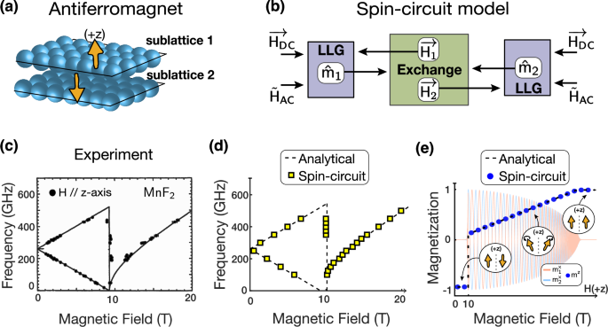
a Sketch of an antiferromagnet where two sublattices with opposing magnetizations. b Spin circuit model of the AFM with two antiferromagnetic layers analyzed by two LLGs coupled with exchange interactions. c Experimental results for AFMR in ({{mathsf{MnF}}}_{2})58. d Numerical results obtained from spin–circuits for AFMR, compared to known theory. e Easy-axis (z) component of the magnetization vector analysis over an external magnetic field applied in the +z direction. At a critical field, the sublattice spins enter the “spin–flop” region, where they both develop a small mz component in the direction of the magnetic field. In all cases, spin–circuits provide excellent agreement with known theory.
By linearizing the coupled LLG equations, two sets of AFMR frequencies can be obtained60,61:
where HK is the uniaxial anistropy of individual sublattices, Hext is the external magnetic field, and γ is the gyromagnetic ratio for the electron. In Fig. 4c, d, we observe that around 10 T, the coupled AFM spins enter the interesting “spin–flop” region where they each develop a small mz component and start processing about this axis (Fig. 4e).
As Fig. 4 shows, all of this physics is captured by the spin–circuit formalism quantitatively. The availability of AC/DC sources, transient and AC simulation options offer a convenient platform to study magnetization physics in a modular manner. The ability to combine such magnetic models with materials and transistors makes the spin–circuit approach appealing.
Engineered antiferromagnets with non-local spin valves
Next, we show an example non-local spin valve (NLSV) setup that couples low-barrier nanomagnets (LBMs) to engineer a “Heisenberg machine” using spin–circuit models. The setup we consider here has recently been proposed theoretically62, and to the best of our knowledge, no experiments involving LBMs and NLSVs have yet been performed. Our main point is that modular spin–circuits can be useful to motivate new experiments, provide quantitative insights into new physics and estimate energy and delay metrics before the physical realization of a proposed system.
In previous sections, we described how we could model magnets by coupling the transport model (F∣∣N) with magnetization dynamics obtained through the sLLG equation. For channel materials used in NLSVs, we now introduce the Normal Metal (NM) model, describing spin–diffusion in channels without any spin–orbit coupling. The NM model consists of a π-network with two shunt conductance Gsh separated by a series conductance Gse as shown in Fig. 513:
where Gc = ANM/(ρNML), Gs = ANM/(ρNMλs)csch(L/λs), and (G{prime} ={A}_{NM}/({rho }_{NM}{lambda }_{s})tanh (L/2{lambda }_{s})). ANM denotes the area, ρNM is the NM resistivity, L is the length, and λs is the spin–diffusion length. These matrices are obtained from microscopic spin–diffusion equations, accounting for the non-conservative nature of spin currents through the shunts.
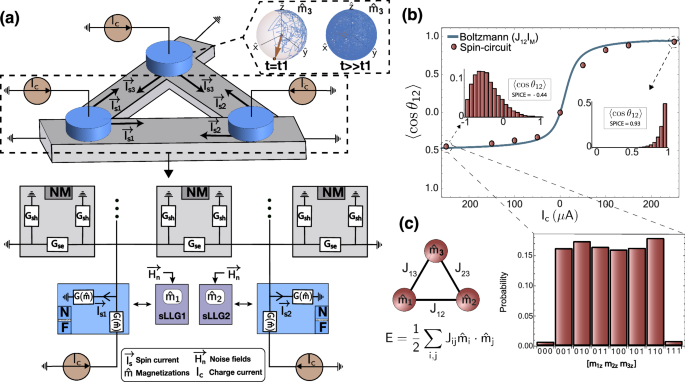
a Physical structure consisting of networks of LBMs. A charge current is injected from LBMs going to a nearby local ground. Spin currents polarized in the direction of fluctuating LBMs are routed to one another. Inset shows an example of how magnetization dynamics (hat{m}) evolve over time for an LBM with low perpendicular anisotropy. The bottom panel shows the spin–circuit corresponding to the physical structure. b The average of the relative angle between LBM 1 and LBM 2 is measured as a function of injected charge currents, showing ferromagnetic (at positive Ic) and antiferromagnetic (at negative Ic) coupling. The numerical results are compared with those obtained from the Boltzmann law obtained from the Heisenberg Hamiltonian. This correspondence between the unitless Heisenberg Hamiltonian and spin–circuit requires a mapping factor IM with units of currents (see text and ref. 62). c A histogram of three LBMs at large negative currents where for better illustration the magnetizations (hat{m}) are binarized by thresholding at ({hat{m}}_{z}=0). The system shows frustration in the antiferromagnetic configuration.
In this example, we stick to spin–isotropic channels without any spin–momentum locking, however, experiments with heavy metals that exhibit Giant Spin Hall Effect63 have been successfully modeled with spin circuits11,20.
The basic idea of the coupled NLSVs in Fig. 5a is to engineer a system of LBMs that interact via pure spin currents. To achieve this, a charge current passes through each magnet with a nearby ground. Then, spin–currents polarized in the instantaneous direction of the magnetization of the LBMs are sent toward neighboring LBMs. The key point is to design a system that takes samples from the classical Heisenberg model:
where Jij are the interaction terms, and mi are 3D-magnetization vectors. Finding low-energy (or equilibrium states of the Heisenberg Hamiltonian for probabilities pi ((propto exp (-E/kT))) is computationally challenging. As such, engineering a system of LBMs to sample from the classical Heisenberg model can be useful for optimization and/or sampling problems. The read-out mechanisms or practical applications of this system are beyond the scope of our discussion here and can be found in ref. 62.
From a modeling perspective, the system shown in Fig. 5a is quite challenging: one needs to model the NLSV transport where charge and spin–currents are modeled properly. Moreover, a self-consistent solution of stochastic LLG equations with transport modules is needed. In the presence of incoming spin–currents that are transport-dependent, the sLLG equations provide magnetization vectors that control the interface conductances. The spin–circuit approach allows a seamless implementation of this highly complicated physical system. As shown in Fig. 5, the magnitude and the sign of the injected charge current control the degree of correlation between two magnets (1 and 2). When the injected charge currents are negative, the coupling between the three LBMs exhibits antiferromagnetic coupling, as shown in Fig. 5c, as would be expected from the engineered interactions obtained from a Heisenberg model with negative couplings.
Functional spin–circuits with transistors
So far, the spin–circuit examples we considered have been based on spintronic building blocks with increasing sophistication, albeit without the use of any transistors. An emerging trend in the field in the beyond Moore era of electronics is the notion of domain-specific computation where conventional, complementary metal-oxide semiconductor (CMOS) transistors are augmented with emerging technologies (({mathsf{X}})) to create CMOS+ ({mathsf{X}}) systems, where ({mathsf{X}}) can stand for anything from spintronics, photonics, memristors, superconducting circuits, and others. In this section, we show how a probabilistic bit with stochastic MTJs combined with CMOS components64,65 can be modeled and characterized within our spin circuit formalism.
Figure 6 shows how a new type of stochastic magnetic tunnel junction can readily be modeled and analyzed using the spin–circuit approach, in conjunction with state-of-the-art transistor models forming a p-bit building block. Typically, magnetic tunnel junctions employ a fixed layer such that the resistance of the junction correlates with the magnetization of a free layer. With the emergence of probabilistic computing66 and the need for fast, energy-efficient, and scalable random number generators, a recent approach has been to design sMTJs with no fixed layers41,67,68.
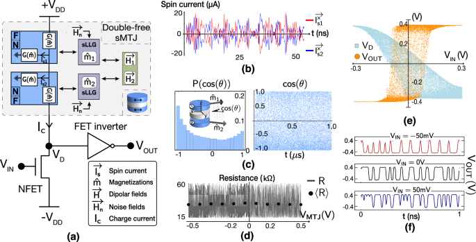
a Self-consistent magnet and transport model combined with transistors to model a probabilistic bit. b Time-dependent spin currents are produced from the transport model that goes into the sLLG modules. We show the x-axis component of spin–currents for magnets, 1 and 2. c Histogram and time fluctuations for the (cos (theta )) between mz components of magnet 1, 2 for the double-free-layer sMTJ. Slight anti-parallel tendency is due to the dipolar coupling which is not completely overcome by thermal fields. d Resistance of the sMTJ is measured while the voltage is swept from −0.5 to 0.5 V over 1 ms. The discrete data points are average resistances over 500 ns showing the roughly bias-independent characteristics of the device. e The drain node (({{mathsf{V}}}_{{mathsf{D}}})) and the output of the inverter (({{mathsf{V}}}_{{mathsf{OUT}}})) are measured while the input (({{mathsf{V}}}_{{mathsf{IN}}})) is swept from −0.3 V to 0.3 V over 1 ms. The output of the inverter shows the binary stochastic neuron behavior. f Digital output fluctuations over time for the probabilistic bit output at different bias conditions for ({{mathsf{V}}}_{IN}).
Typically, physics-based device models cannot easily be interfaced with transistor models, whereas the SPICE formulation of spin–circuits allows seamless integration with CMOS. Figure 6 shows such a combination where a spin–valve made out of two LBMs is connected to an n-MOS transistor. Here, we use FinFET models from the open-source predictive technology models (PTM)69, in principle, however, any other FET model could be combined with spin–circuits. When we combine spin–circuits that carry 4-component currents and voltages with ordinary circuits that only carry charge currents, we only attach the charge current terminals to each other, since any other spin information can be ignored in extended charge circuits. The double-free layer sMTJ exhibits an interesting voltage-independent resistance profile70. This behavior is reproduced by the spin–circuit model where the two symmetric layers receive spin–currents with opposing signs (Fig. 6b), leading to nearly uniform fluctuations (Fig. 6c) and weak voltage-bias dependence (Fig. 6d). Voltage bias independence is shown to be favorable in p-bit circuitry to obtain a clear sigmoidal response in the face of device-to-device variations. The slight asymmetry favoring an anti-parallel configuration stems from the dipolar coupling between the easy-plane magnets, which is included in the spin–circuit simulation (following the methodology in ref. 67). Later work suggests that building sMTJs out ofsynthetic antiferromagnet (SAF)-based free layers can remove this zero-field dipolar coupling entirely41.
Finally, Fig. 6e, f shows the full input–output characteristics of what has been called a probabilistic or p-bit71 that is obtained from our full model. These simulations demonstrate the tunability of randomness at different bias voltages. An important point to stress is that the tunability does not arise from spin–transfer–torque effects modulating the free layer magnetizations, but rather from the changing transistor conductance by an analog input voltage.
The combination of magnetization dynamics, dipolar and thermal noise fields, 4-component interface conductances, and transistors in a sound powerful circuit simulator shows the power and flexibility of the spin–circuit approach. We believe the approach eases the prediction and device-circuit level evaluation of new types of spintronic devices. In the case of double-free-layer sMTJs (first with double-free layers67 and then with double-free SAF layers41), spin–circuit theory predicted the key qualitative features of these devices that have later been experimentally demonstrated42,70.
From spin–circuits to systems
So far, the spin–circuit examples we illustrated are all at the device or the circuit level. The combination of spin–circuits with transistors unlocks a much larger space of possibilities including the realization of energy and area-efficient p-bit networks. As a final example, we describe a hybrid system where a true random number generator (TRNG) augments a low-quality pseudo-random number generator (PRNG) (even though our modeling in SPICE will use PRNGs for the sMTJ part of this circuit, the RNG quality used for this purpose will be much higher than that of an LFSR without noticeable differences between an actual MTJ, see ref. 65 for details). Figure 7 shows the p-bit circuit from Fig. 6 triggering a digital p-bit (Fig. 7a, b) to generate a tunably random behavior (whose average is shown in Fig. 7c).
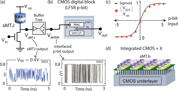
a An sMTJ-based binary stochastic neuron (p-bit) is interfaced with a digital CMOS-based circuit to trigger a digital p-bit emulator. The bottom panel shows SPICE results for the analog fluctuations at the drain (VsMTJ) of the NMOS transistor. b Rail-to-rail stochastic fluctuations are obtained after a buffer tree (VINTER) is inserted between the single sMTJ-based p-bit and the large digital CMOS block. CMOS block contains a low-quality and inexpensive pseudo-random number generator (PRNG) along with a look-up table to obtain tunability. This hybrid setup with the sMTJ circuit increases the quality of randomness that can be obtained from the digital p-bit block alone (see ref. 65). c Tunability of the heterogeneous structure as a probabilistic bit is shown with time-averaged VOUT over 1000 ns in SPICE. d In the future, millions of sMTJs can provide nearly-free true randomness to CMOS underlayers for various probabilistic computing applications.
The motivation is to increase the quality of randomness that is extracted from inexpensive linear feedback shift register (LFSR)-based PRNG by clocking the PRNG with random arrivals of sMTJ fluctuations. This setup was realized using physical sMTJs in a recent experiment that established the concept65. Considering the expensive nature of PRNGs, augmenting them with the true randomness of millions of sMTJs in integrated CMOS+ ({mathsf{X}}) systems (Fig. 7d) seems desirable.
The CMOS block consists of a PRNG and a lookup table (LUT) for the hyperbolic tangent function consisting of thousands of transistors. The CMOS design is synthesized from the open-source ASAP7 Predictive PDK72 and the details of how this synthesis is performed can be found in ref. 65.
The bottom panels of Fig. 7 show simulations obtained from this hybrid circuit where a single sMTJ-based circuit drives thousands of transistors. An important detail, immediately captured by the spin–circuit approach is that of loading. Without a “buffer tree” where several stages of inverters distribute the capacitive load of the CMOS p-bit that is seen by the single sMTJ-based circuit, the clocking does not work. These nontrivial loading effects at the interfaces of physics-based and digital systems are naturally captured by the powerful spin–circuit approach that is otherwise easy to miss. In addition to loading, key circuit and system metrics such as energy delay can be reliably calculated for many types of exploratory systems.
To verify the functionality of the synthesized p-bit, we probe the drain voltage in Fig. 7a to observe the sMTJ random telegraph noise when biased at V50/50, followed by the rail-to-rail output of the buffer tree in Fig. 7b. In Fig. 7c, we plot the probability of the p-bit output being 1 against the decimal equivalent of p-bit input, matching the expected sigmoidal behavior. This system represents an energy-efficient and scalable p-bit model, which has demonstrated significant potential in offering scalable solutions to complex, previously intractable problems65,66.
Conclusion
We have described the spin–circuit approach connecting the microscopic physics of spins and magnets all the way up to circuits and systems. We believe that such a physics-based, modular, CMOS-compatible modeling approach will be critical in evaluating and exploring new hardware systems in the beyond-Moore era of electronics. Despite the wide focus of this paper, there are many other spintronic phenomena that have been modeled by spin–circuits, and we did not get into these, e.g., full compute life-cycle modeling of skyrmions and domain walls73. Beyond spins, a similar circuit framework for new and emerging phenomena can be constructed. Extensions may include pseudospins, valley currents30, superconductivity, photonics, and qubit systems74. A diverse set of such phenomena can all be analyzed within the context of powerful, industry-standard transistor-compatible circuit simulators while being rigorously connected to the underlying physics beyond empirical compact models. In the new era of electronics, such extended spin–circuits could enable a rapid and robust evaluation of emerging CMOS+ ({mathsf{X}}) systems.
Responses