Improving the thermoelectric performance of scandium nitride thin films by implanting helium ions
Introduction
Transition metal nitrides (TMNs) thin films have been widely studied in the past decades for a wide range of applications1,2,3,4,5, taking advantage of their excellent mechanical6,7, plasmonic8,9, piezoelectric10,11 and, more recently unveiled, thermoelectric properties11,12,13. Among them, ScN was extensively investigated as it exhibits a semiconducting behavior with an indirect bandgap of 0.9 eV and direct bandgap of 2.2 eV14,15,16,17,18,19, a high hardness of 21 GPa20, a substantial wear corrosion resistance and an elevated melting point standing above 2600 °C11,21. Unlike conventional III-V nitride semiconductors, ScN crystallizes in a NaCl structure-type with an octahedral Sc coordination, leading to N 2p orbital dominance at the top of the valence band and predominant Sc empty 3d t2g states at the bottom of the conduction band22,23,24,25. While it is well known that native defects such as N vacancies and incorporated impurities like ON substitutions can alter the electronic band structure, it turns out that the latter is relatively rigid25. Consequently, such defects only impact the position of the Fermi level, freely shifting towards valence or conduction bands depending on the nature of the doping. As N vacancies or unwanted impurities like O or F act as electron donors, the Fermi level lies in the conduction band, leading to n-type degenerate semiconducting behavior in most sputter-deposited ScN films. The reported carrier densities fall in the 1018 – 1022 cm-3 range, mainly depending on the O at. % incorporated during deposition22,25,26,27,28. Unwanted O impurities are hardly avoidable, owing to both a low, negative ON formation energy, and a high affinity of Sc with O24.
In the last decade, a number of studies have proved ScN to be a promising low dimensional thermoelectric material13,23,26,27,28,29,30,31. Thermoelectric materials allow the direct conversion of thermal energy into electricity using the Seebeck effect, the process being reversible32. The thermoelectric performance of such materials is assessed by the figure of merit zT = S²T/ρ(({kappa }_{e}) + ({kappa }_{L})), S being the Seebeck coefficient, ρ the resistivity, ({kappa }_{e}) the electronic thermal conductivity, ({kappa }_{L}) the lattice contribution to the thermal conductivity and T the absolute temperature. The improvement of the figure of merit often arises from a reduction of the thermal conductivity while maintaining favorable electrical transport properties through a maximized power factor PF = S²/ρ32. The reported power factors for n-type ScN are as high as 2–4 mW·m−1·K−2 at about 800 K13,23,26,27,28,30,31, competitive with current state-of-the-art materials such as Bi2Te333, PbTe34, or SiGe35 in their respective temperature range. The thermal conductivity of ScN, however, is relatively high with a value of about 12 W·m−1·K−1 at room temperature, preventing ScN to exhibit competitive zT values so far (0.2‒0.3 at 800 K)11,13,22,31. Attempts to reduce the thermal conductivity was conducted by alloying ScN with several metals such as Mg or Nb but resulted in either no thermal conductivity reduction (Mg doping)30 or degradation of electrical properties (Nb doping)36, preventing further zT improvements.
An effective way to reduce the thermal conductivity is to introduce defects in the material. That can be done by taking advantage of the ion implantation technique in low dimensional materials. The ion implantation process is particularly interesting for thermoelectric outcomes as it leverages from two beneficial synergistic effects: (i) the fine tuning of the charge carrier concentration by controlling the implanted dopant doses, and (ii) the reduction of the lattice thermal conductivity through phonon scattering by inducing point defects or nanocavities. Studies conducted on implanted/irradiated nanosized silicon, where the nature and behavior of generated defects are well understood, have demonstrated that these defects can effectively reduce or even control the lattice thermal conductivity37,38. Furthermore, this technique has already proved to be truly promising to improve thermoelectric properties, as recently reported39,40,41,42,43,44,45,46.
The thermoelectric properties of irradiated and implanted ScN with different ions were investigated in recent years. Tureson et al. have implanted Mg+ in (111) ScN grown on c-sapphire substrate, where a notable threefold thermal conductivity reduction was observed after room-temperature implantations47. An irradiation of ScN thin films by Li+ ions was conducted by Rao et al., yielding a halved thermal conductivity in the 300–950 K temperature range46. The power factor was maintained at a decent value of about 1–2 mW·m−1·K−2, resulting in an overall preserved figure of merit. More recently, an implantation of non-electrically active argon ions into ScN thin films at room temperature resulted in a drastic reduction of the thermal conductivity, from 12.5 to 3 W·m−1·K−1 at 300 K for as-implanted samples45. The use of heavy noble gas ion was motivated by the large ballistic effects providing both point defects and extended defects48. Noble gas are indeed known to form complex-like defects with atomic vacancies49,50,51, further adding scattering centers for phonons and thus having a strong impact on the lattice thermal conductivity. Complex-like defects result from the aggregation of vacancies, leading to vacancies clusters which are stabilized by the presence of implanted helium atoms50. The electrical transport properties were strongly impacted, and subsequent high temperature annealing revealed a partial recovery of the defects, demonstrating the extensive impact of defect recombination on the transport properties45.
Ion implantation has shown potential as an effective technique for enhancing thermoelectric properties by introducing defects in materials, although the specific mechanisms governing these improvements remain to be fully elucidated. Building on previous work with argon-implanted ScN thin films45, we extend this investigation to helium, a lighter noble gas. Given the significant differences in mass and radius between argon and helium, differences in implantation-induced defects and their subsequent effects on transport properties could be expected. SRIM simulations confirm that each argon ion creates over ten times more vacancies than helium ions, suggesting that the lighter helium could lead to distinct defect characteristics and thermal behavior.
In this study, we investigate the electrical and thermal transport properties of helium-implanted ScN thin films, with a particular focus on the stability of implantation-induced defects under different annealing conditions. By correlating these properties with microstructural changes observed through electron microscopy, we aim to shed light on how helium implantation affects defect formation and recovery. Ultimately, we identify the optimal annealing process that maximizes the thermoelectric performance of ScN films, providing new insights into the role of defect engineering in enhancing material properties for thermoelectric applications.
Results and discussion
According to ERDA characterization, the composition of the as deposited film is estimated to be ScN0.95(1) with the presence of about 3.5(2) at. % oxygen content. At this doping level, a degenerate semiconducting behavior is expected due to the shifting of the Fermi level in the conduction band. Structural characterizations by means of Transmission Electron Microscopy (TEM) were carried out on the reference sample as shown in Fig. 1, and confirmed the epitaxy of the (111) oriented ScN film on the (0001) Al2O3 substrate, including the presence of twins due to the epitaxial relation between the film and the substrate. Further details on the microstructure of the reference film are reported in a previous study45.

a Bright field TEM micrograph of a reference sample of ScN thin film deposited on a Al2O3 substrate. The columnar nature of the two growth variant type grains can be observed in the inset a. Electron diffraction patterns of both ScN and Al2O3 are displayed in the inset b and c, respectively, confirming the epitaxy relationship between the film and the substrate.
Figure 2 presents a TEM micrograph of the ScN film implanted with He ions at a damage level of 1 displacement per atom (dpa). Diffuse black dots can be observed, suggesting the presence of He implantation-induced defects. The diffraction picture recorded from this micrograph indicates that no part of the sample was amorphized, the crystallinity of the film being preserved as shown by the well-defined diffraction spots and the absence of amorphous rings (Fig. 2b). The columnar nature of the film grains is also maintained, with well-defined grain boundaries, despite the clear presence of defects.

a Bright field micrograph, b Electron Diffraction pattern of the area along the zone axis [(bar{1}10)].
Figure 3 presents the temperature dependence of electrical resistivity and mobility for both reference and helium-implanted ScN films. As expected, the reference sample exhibits metallic conductive behavior, typical of a degenerate semiconductor, due to high doping levels resulting from the presence of oxygen impurities. The charge carrier concentration remains constant throughout the temperature range, with a value of 2.2(2) × 1021 cm−3, consistent with previously reported studies on ScN films grown under the same conditions45,48. After helium implantation, a notable shift in conduction mode was observed, with the resistivity decreasing as temperature increases—a behavior also seen in argon-implanted films with the same damage level (1 dpa)48.

Resistivity (a) and charge carrier mobility (b) measurements of the ScN reference and He-implanted films. Point-like defects induced by implantation of He ions are recovered when a temperature of approx. 750 K is reached, similar to Ar-implanted ScN thin films43. The charge carrier concentration were measured to be constant over the whole temperature range. Double arrows indicate that the measurements are reversible while single arrows characterize irreversible measurements due to partial defect recovery. Standard deviations are 4% and 5% for the resistivity and mobility, respectively.
Two types of defects emerged after helium implantation: point-like defects and complex-like defects. The data in Fig. 3 shows two measurements from 80 K to 750 K performed successively, the second measurement thus being conducted after an in situ annealing at 750 K, a temperature where the point-like defects have recovered. In region I (Measure #1, T < 400 K), the resistivity and mobility are cyclable, indicating that point-like defects concentration remains constant. As the temperature exceeds 400 K (region II, 400 K < T < 720 K), point defects start to recover, resulting in irreversible changes to transport properties. At temperatures above ~720 K (region III), only complex-like defects remain and dominate the resistivity and mobility. Once the point defects have fully recovered, metallic-like behavior is restored, as seen in the second set of measurements (Measure #2, Fig. 3a). In region I, both point-like and complex-like defects influence transport, while in region III, only complex-like defects remain active. Point-like defects mainly affect the conduction mechanism, whereas complex-like defects act as charge trapping. Indeed, the charge carrier concentration remains constant at 1.0(2) × 1021 cm−3 across the 80–750 K range, indicating that the ~50% reduction in carrier density results exclusively from complex-like defects: point-like defects do not act as carrier traps45,48. The point defects only affect the conduction mechanism and also contribute to a decrease in electron mobility (Fig. 3b)48.
These findings indicate that helium implantation has similar effects on transport properties as those observed previously with argon implantation, in particular concerning the changes in conduction mode48. It should be noted that despite substantial differences in concentration (0.05% for Ar and 1% for He) and atomic mass (40.0(1) AMU for Ar and 4.0(1) AMU for He) between the two studies, the nature of the implantation-induced defects remains quite similar. On the other hand, these experiments were conducted at the same damage level of 1 dpa. Therefore, the influence of ion implantation on the electrical transport properties appears to be primarily governed by the level of damage introduced in the material rather than the quantity/type of the noble gas implanted.
To further understand the conduction mechanism, the resistivity was plotted as ln (ρ) = f(1/T) (Fig. 4a) and ln (ρ) = f(1/T1/4) (Fig. 4b) and different models were fitted and compared with the literature. The as-implanted resistivity can be fitted with an Arrhenius law in the region II (Fig. 4a), yielding an activation energy of the point-defect recombination of 130(10) meV. That value is slightly larger than the activation energy of the point defect recombination generated by Ar or Mg implantation ions (about 90 meV for both)47,48. In addition, the fitting of the ln (ρ) = f(1/T1/4) curve in the low temperature range (region I) with a Variable Range Hopping model as proposed by Mott and Davis52, yielded a Mott temperature of TM = 5 K (Fig. 4b). This value is in the same order of magnitude than that of Ar-implanted ScN films with an equivalent damage level of 1 dpa (TM = 1 K). According to Mott’s model, the Mott temperature is related to the localization parameter Lc of the defects as TM ~ A /(NF Lc3), (A being a constant and NF the density of states at the Fermi level). Consequently, the increase in the Mott temperature suggests a decrease in the localization parameter Lc, calculated to be approximately 36 nm based on an estimated density of states N(EF) of about 1021 eV−1·cm−3, according to the calculations of the position of the Fermi level by Mu et al.53. Hence, it can be deduced that the He-implanted films exhibit a slightly larger defect density than Ar-implanted films despite the large difference in gas concentration. This is consistent with the fact that the Mott temperature increases with the fluence, hence with the number of implanted ions and generated defects54. Conversely, TM is reduced when the film undergoes an in situ annealing (between 400 K and 750 K) due to the recombination of the defects. These differences motivated further investigation into the microstructural properties of the He-implanted ScN.

a ln(ρ) = f(1/T), yielding an energy activation of the defect recovery process of EA = 130 meV, b ln(ρ) = f(1/T1/4), fitted using a Mott law, unveiling a Variable Range Hopping (VRH) conduction behavior with a Mott temperature of TM = 5 K.
TEM micrographs of the as-implanted ScN film with helium ions in bright field, out of zone axis and in Fresnel conditions are presented in Fig. 5. By playing with the focus, the presence of nanocavities of about 10–20 nm, eventually resulting from He bubbles, can be detected. Such cavities are dispersed along the growth direction, suggesting that these inclusions are favored near the grain boundaries. These cavities are thus formed in the He as-implanted ScN films, while being only observed after high-temperature annealing in the case of Ar-implanted ScN45. Noble gases are known to form complexes with vacancies within implanted solids, forming voids or bubbles upon aggregation that occurs either during implantation or upon post-implantation thermal treatment55. It is reasonable to assume that the formation of vacancy-noble gas complexes is favored in the case of He due to (i) the large number of available vacancies and the mobility of helium (lower atomic radius rHe = 0.31 Å compared to rAr = 0.71 Å), and (ii) the concentration of He ions used (~1%) being 20 times larger than that of Ar (~0.05%) for an equivalent level of damage (1 dpa). The presence of such complexes, which are considered precursors to cavity formation and are favored near grain boundaries, accounts for the formation of nanometric cavities in these regions.

a Under-focused and b over-focused bright field micrographs, unveiling the presence of nanocavities (5–20 nm) induced by He species on the as-implanted sample. The cavities are aligned with the grain growth, suggesting that their formation is favored in the grain boundaries regions.
The presence of nanocavities in the film after He-implantation are expected to have a significant impact on thermal properties, as nanoinclusions are well-known to act as scattering centers for phonons56. Furthermore, annealing the sample at high temperatures is anticipated to affect these cavities through thermally activated diffusion mechanisms. Figure 6 shows a TEM micrograph of the He-implanted sample annealed at 1273 K. After high temperature annealing, the nanocavities remain present with a notable increase in size, evidenced by the presence of larger, aggregated cavities of approximately 40 nm (compared to 5–20 nm before annealing). Their formation is still favored along the grain growth direction explained by an easier diffusion along the grain boundaries.

Bright field micrographs under 3-waves configuration, showing the presence of the He-implantation-induced nanocavities. The cavities distribution in the film is still aligned along grain boundaries. However, the density of nanocavities has increased compared to the as-implanted sample.
The investigation of the complete transport properties of the as grown and annealed implanted ScN films with different thermal treatment is presented in the following sections to assess the influence of such inclusions and their thermal history on the thermoelectric properties.
The temperature dependence electrical resistivity and the electron mobility from the reference ScN film, He-implanted and annealed at various temperatures samples are depicted in Fig. 7. The so-called in situ annealing sample refers to the sample measured once up to 750 K (Fig. 3). The electron mobility of the 750 K in situ annealed (few seconds) film and the 673 K annealing (10 min) film are very similar, the slight differences between these two samples being attributed to the kinetics of defect recovery. Annealing at higher temperatures (1273 K) provokes a recovery of complex-like defects, leading to further recovery of the electrical resistivity and carrier concentration close to those of the reference film. Despite the recovery of charge carrier concentration, the electron mobility remained unchanged compared to the in situ annealed sample. The reduced and unchanged mobility of the annealed samples suggested that residual microstructural defects, such as cavities (Figs. 5 and 6), persist in the sample and act as scattering centers for electrons.

a Resistivity and b mobility curves of the ScN Reference (black), He-implanted and in-situ annealed at about 750 K (point-like defects recovered – red), He-implanted then annealed at 673 K (blue), and He-implanted then annealed at 1273 K (green) films. The charge carrier concentrations were measured to be constant over the whole temperature range. Standard deviations are 4% and 5% for the resistivity and mobility, respectively.
To understand further the scattering mechanism resulting from the presence of such cavities and nanostructure, a modeling of the mobility curves was performed according to the Matthiessen law displayed in Eq. (1) with (mu (T)) the temperature dependent mobility, and ({mu }_{{Latt}}(T)), ({mu }_{{GB}}(T)), ({mu }_{R}), and ({mu }_{D}) the lattice, grain boundaries’, residual impurities’ and implantation-induced defects’ contributions to the mobility, respectively.
The fitting of the as-grown reference ScN curve indicates that the electron mobility is primarily driven by electron-phonon interactions (µLatt (T) = β T−3/2) and residual impurities (({mu }_{R}=14-15) cm2·V−1·K−1). The grain boundaries (({mu }_{{GB}}(T))) appeared to be negligible, which is consistent with a recent study on the electron mobility in ScN57. The implantation of He results in a drastic reduction in mobility, which becomes almost constant over temperature (Fig. 8). The modeling of this curve could be accurately carried out adding a supplementary term in the Matthiessen’s law (({mu }_{D}=8-9) cm2·V−1·K−1), which dominates the mobility scattering mechanisms. High-temperature annealing at 1273 K results in a slight increase in this value (({mu }_{D}^{1273}=10-11) cm2·V−1·K−1) and alters the lattice mobility pre-factor (β). This is consistent with the structural changes and their evolution upon subsequent annealing observed by TEM analysis. Hence, the presence of nanocavities and localized defects play a dominant role in the charge carriers scattering mechanism and explains well the large reduction in mobility observed after implantation of helium species. This dominant contribution might be enhanced by the surface of the nanocavities as it was shown that the edges of nanocavities under the form of pores are dominating the scattering mechanism of electrons58.

a Seebeck coefficient and b Power factor of the ScN reference (black), He-implanted after recovery of point-like defects (in situ annealing at about 750 K, red), He-implanted then annealed at 673 K (blue), and He-implanted then annealed at 1273 K films (green). Standard deviations are 6% and 15% for the Seebeck coefficient and the power factor, respectively.
The Seebeck coefficient and power factor are displayed in Fig. 8. The absolute values of the Seebeck coefficient for all samples increase linearly with temperature, which is consistent with the degenerate semiconductive behavior. The absolute Seebeck coefficient of the He-implanted sample was doubled on the whole temperature range, reaching ‒80 µV·K−1 at 673 K, compared to ‒46 µV·K−1 for the reference at the same temperature. It can be noted that the absolute value of the slope is increased by about 80% after implantation and an in situ annealing at 750 K (red data in Fig. 8. This observation is consistent with the decrease of the charge carrier concentration after implantation which was halved. A decrease in the slope of the Seebeck coefficient was also observed in the case of Ar-implanted ScN films, the latter being however more pronounced (decrease by a factor of 3) while the charge carrier concentration was also halved after implantation45. This little difference might be explained by the fact that the complex-like defects arising from the coupling of vacancies with the noble gas (NGn Vm, n < m, NG = Ar, He), although similar in nature, induce a slightly different effect on the density of states and therefore on the electrical properties of the film. Helium atoms, trapped by the vacancy complexes, are present in a substantially higher quantity than in the case of argon implantations, due to the higher implanted concentration of the former compared to the latter. Therefore, the defects generated in the case of He are expected to have a more localized influence, which would lead to a less affected DOS near the Fermi level, explaining the slight difference in the Seebeck coefficient slopes when compared to Ar implanted ScN films45. A modest variation of the slope is observed after the annealing at 673 K, in line with the slightly decreased charge carrier concentration and mobility. However, the sample annealed at 1273 K exhibited comparable values as the reference sample. Interestingly, it can be noted that despite the very limited recovery of mobility and partial recovery of resistivity, the Seebeck coefficient is fully recovered, same as the charge carrier concentration. This result might be attributed to the fact that the density of states (DOS) near the Fermi level is not significantly modified, leading to a similar electron effective mass between the reference and the high-temperature annealed sample. On the other hand, the presence of larger size, aggregated cavities and nano-inclusions as observed in TEM micrographs after high-temperature annealing are responsible for the strong reduction of the mobility, leading to an overall increased resistivity. The resulting power factor of all samples are presented in Fig. 8. Due to resistivity rises, the power factor of the 750 K in situ annealed sample and the 1273 K annealed sample is lowered by about 18% and 42% at 600 K, respectively. However, the sample annealed at 673 K presents a very similar power factor than that of the reference film, suggesting that the microstructure of the sample at this stage, which includes small size nanocavities (about 5–20 nm), does not reduce the electrical transport properties performance.
The thermal conductivities of all samples were measured at room temperature using the modulated thermoreflectance technique. Detailed information on the fitting models of the thermoreflectance data and subsequent analysis can be found in the Methods section. The resulting thermal conductivities at room temperature are depicted in Fig. 9a, along with their lattice and electronic contributions. The reference sample exhibits a thermal conductivity of about 13(1) W·m−1·K−1, consistent with values reported in the literature30,36,47. Although the lattice thermal conductivity is dominant, the electronic contribution is significant (~23%) due to the degenerate semiconducting behavior, where free electrons substantially contribute to thermal transport. Upon implantation, the thermal conductivity is significantly reduced to a value of about 7(1) W·m−1·K−1, marking a 46% drop. This large decrease of the thermal conductivity after ion implantation is expected and has been previously reported in the literature40,42,43,44,45,46,47,59. In the present implanted ScN samples which were in situ-annealed at 750 K, annealed at 673 K and annealed at 1273 K, only complex-like defects and nanocavities are remaining in the films. As shown in Fig. 10a, both the lattice and electronic contributions to thermal conductivity are significantly impacted by those induced defects by ion implantation, acting as efficient scattering centers and strongly reducing the thermal conductivity. Complex-like defects, being much smaller than nanocavities (10–40 nm), predominantly scatter short-wavelength phonons, playing a dominant role in reducing the lattice thermal conductivity by effectively disrupting phonon transport within the grains56,60. In contrast, nanocavities scatter long-wavelength phonons due to their larger size. However, their contribution to lattice thermal conductivity reduction appears to be rather limited in this study. Despite the persistent presence of nanocavities after high-temperature annealing (1273 K), the lattice thermal conductivity is almost fully recovered at about 10.5(10) W·m−1·K−1, suggesting that long-wavelength phonons contribute minimally to overall phonon scattering in these sample series.

a Thermal conductivity and b figure of merit zT of the Reference (black), He-implanted then in situ annealed at about 700 K (red), implanted then annealed at 673 K (blue), and implanted then annealed at 1273 K samples at room temperature (green). The lattice and electronic contributions to the thermal conductivity are displayed. Standard deviations are 13% and 20% for the thermal conductivity and zT, respectively.
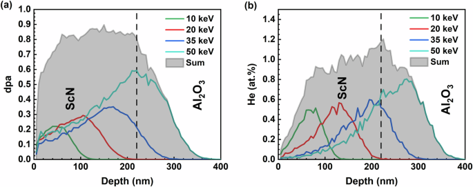
a Displacement per atom (dpa) and b concentration profiles as function of depth, calculated using SRIM code for a cumulative multi-energy He-1dpa implantation – 10 keV (green), 20 keV (red), 35 keV (dark blue), 50 keV (light blue) and the sum (gray).
Nanoinclusions, on the other hand, have a more pronounced effect on the electronic thermal conductivity. After annealing at 1273 K, the electronic contribution remains halved (about 1.5 W·m−1·K−1) compared to the reference sample, consistent with significant charge carrier scatterings at nanoinclusion surfaces, reducing the carrier mobility. The recovery of the complex-like defects after high temperature annealing leads to a partial restoration of the thermal conductivity, up to k ~ 10.5(10) W·m−1·K−1 for the sample annealed at 1273 K, as the scattering effects of these defects are suppressed. Overall, the cumulative effects of these scattering mechanisms lead to the observed strong reduction in thermal conductivity, primarily dominated by the presence of complex-like defects.
The thermoelectric figure of merit zT of corresponding samples are displayed Fig. 9b. Note that zT values presented in this study are used to compare the sample series and evaluate the relevance of the ion implantation and annealing conditions on the thermoelectric properties of ScN thin films. zT values are calculated from electrical properties that are measured in the in-plane direction while thermal conductivity measurements are performed in the cross-plane direction and most probably deviate from real values. Consequently, the absolute zT values must be taken with great care. However, the measurements being processed the same way for all samples, zT values can be compared. The implanted film experienced a 28% increased zT value with respect to the reference sample, owing to the large presence of defects which strongly reduce the thermal conductivity without reducing too much the power factor. As the PF is even greater for the sample annealed at 673 K, the zT further increased to an almost double value compared to the reference. The defects generated from a chemically inert He ion-implantation are thus sufficient to tune the transport properties in such a way that the overall thermoelectric performance is enhanced. On the other hand, an annealing at 1273 K induced a reduced power factor and recovered thermal conductivity, leading to a decreased zT value with respect to the reference. Therefore, a high temperature annealing (1273 K) of the He-implanted ScN films at 1 dpa is not beneficial for the thermoelectric performance of the films.
Conclusion
The structural and transport properties of ScN thin film deposited on Al2O3 substrates and implanted with chemically inert He ions were investigated for potential thermoelectric outcomes. A constant level of damage of 1 dpa was applied throughout the film to evaluate its impact on the properties, leading to a He concentration of about 1 at.%. TEM characterizations revealed the presence of interstitial clusters and nanocavities formed after agglomeration of He-vacancies complexes. Such cavities were present right after implantation, contrary to the Ar case, and were favorably formed in the grain boundary regions, thus following the same direction as that of the columnar grain growth. As high temperature annealing was performed, both structural and transport properties were affected, the transport being strongly dependent on the annealing temperature. Exhaustive investigation of the transport properties in each case revealed that the resistivity is manifold increased for all samples, mainly due to a strongly reduced mobility. The charge carrier concentration was reduced by half after implantation due to complex-like defects acting as trap carriers, releasing the electrons after their full recovery at 1273 K. That leads to a Seebeck coefficient identical to the reference sample, contrary to the implanted and 673 K annealed sample which exhibits about doubled Seebeck values. Consequently, the power factor was preserved for the sample annealed at 673 K, the rise of resistivity being compensated by the increased Seebeck coefficient. On the other hand, the thermal conductivity was strongly reduced for all samples, owing to defect clusters and nanocavities. That leads to significantly improved zT values, with a doubled value for the sample annealed at lower temperatures (673 K). This quite unexpected result appears truly promising as this technique can be applied to any low dimensional materials and thus opens a large window for improvement of any thermoelectric thin film. Taking advantage of chemically active species, it can be assumed that further transport properties optimization could be achieved by wisely choosing the nature of the doping ions and the implantation parameters. The ion implantation technique hence stands as a promising technique to improve the thermoelectric properties of state-of-the-art low dimensional materials.
Methods
Thin film growth and composition analysis
Epitaxial-like thin films of ScN were deposited using dc reactive magnetron sputtering in an ultra-high-vacuum chamber (base pressure 10−6 Pa), onto c-sapphire substrates maintained at 800 °C. The detailed deposition process and system is further described elsewhere47,61. The ScN films show a high electron concentration of about 1021 cm−3 due to the presence of unwanted oxygen impurities incorporated during deposition. Elastic recoil detection analysis (ERDA) characterizations were performed to assess the composition of the films, in particular determine the level of incorporation of any unwanted impurities. A 36 MeV 127I beam was employed, with incident primary ions and recoiling species striking and exiting the sample at an angle of 67.5° to the surface normal, respectively. The Potku software package62 was used to calculate the relative atomic concentration from the recorded ERDA spectra.
Implantation conditions
The 220 nm thick films were ion-implanted at room temperature using a EATON VN3206 implanter. The samples were characterized before implantation to allow comparison and assess the evolution of the structure and transport properties. The depth profiles of the implanted ions in the ScN films were simulated using SRIM 2013 software under the full-damage cascade63. A multi-energy implantation protocol was used to introduce a constant quantity of damage (called displacements per atom, noted dpa) as a function of the film depth. The level of dpa, in the range 0.8–1 dpa, was controlled by the fluences of incident ions. The energy profile extracted from SRIM 2013 simulations with helium ions is presented in Fig. 10, using four decreasing incident energies of 50, 35, 20 and 10 keV with fluences of (12times {10}^{15}), (6.4times {10}^{15}), (4.8times {10}^{15}) and (3.2times {10}^{15}) ions·cm−2, respectively. These implantation parameters allow the introduction of a constant damage level into the film (reported as 1 dpa in the next sections for clarity), the concentration of helium atoms introduced fluctuating around 1 at.%. All implantation parameters are regrouped in Table 1.
Transport properties characterizations
The in-plane electrical resistivity ρ and charge carrier concentration n were measured in the Van der Pauw configuration using an ECOPIA HMS-5500 Hall measurement system in the 80–750 K temperature range. Hall measurements were performed using a constant magnetic field of 0.580 T. The carrier mobility was extracted using the relation µ = 1∕neρ, e being the elemental charge. The Seebeck coefficient was measured up to 680 K in a classical linear four-probe configuration on a ULVAC ZEM3 apparatus using a thin film designed sample holder. High-temperature sample annealing was carried out in a home-made lamp furnace under vacuum during 10 min with a heating rate of about 20 °C.min−1.
Transmission electron microscopy
TEM micrographs were obtained from a TALOS F200S Thermofisher microscope with a tension of 200 kV. Cross-section TEM samples were prepared on an FEI ThermoFisher Helios Nanolab 660 by using the standard lift-out technique. The thickness was then further reduced using a Precision Polishing Precision System (Gatan-PIPS) to reach sufficiently thin samples.
Thermal conductivity characterization
Modulated Thermo-Reflectance (MTR) microscopy characterizations were carried out to determine the thermal conductivity of the samples64. In this optical and non-destructive method, an intensity-modulated Laser (Pump) beam is focused on the surface of the sample (Objective X50 NA 0.5) at a frequency of 100 kHz, resulting in a modulated thermal response from the sample. Another probe Laser spatially scanning the sample measure its reflectance by fetching the signal back in a photodiode. The AC reflectance component recorded by a lock-in amplifier yields a signal characterized by a given amplitude and phase characteristic of the thermal properties of the sample. The probe beam signal is fitted by a multilayer thermal diffusion model, allowing the determination of the thermal conductivity and other thermal properties of the sample such as the specific heat and interfacial thermal resistance. The modulation frequency was set at 100 kHz. The wavelength of the pump and the probe Lasers were 532 and 488 nm, respectively. A thin transducer layer of gold was deposited on each sample (~60 nm) to maximize the probe’s sensitivity to the thermal field.
The amplitudes and phases measured by MTR are leveraged to determine the thermal conductivity of all samples (Fig. 11). Clear differences can be observed between the samples, suggesting different thermal characteristics, consistent with both structural and electrical properties evolution described in the article. In particular, a broadening of both the amplitude and phase of the implanted sample is observed, which is consistent with a decreased thermal conductivity of the film layer.

a Amplitudes and b phases of modulated thermoreflectance measurements performed on the ScN Reference, as-implanted, implanted then annealed at 673 K, and implanted then annealed at 1273 K films.
As the sample was annealed, a recovery of both curves can be observed towards the reference ones, suggesting a recovery of the thermal conductivities. Detailed fittings of the curves were performed by a multi-layer model to accurately assess the thermal transport properties of the samples. Fitting curves according to this model applicated for the sample annealed at 1273 K is presented in Fig. 12. The measurements of all samples were fitted using the same method, considering the transducer layer (gold, ~60 nm thickness), the ScN film thickness (220 nm), the reduced thermal conductivity of the Al2O3 substrate near the interface, and all thermal resistance interfaces. The equivalent thermal resistance is defined as Req = thickness/thermal conductivity. In particular, the thermal resistance interface between the transducer layer and the ScN film was fixed as constant for all samples (Req = 0.167 × 10⁻⁸ m2.K.W−1). The thermal properties of the substrate were also considered as constant (with tabulated values of Al2O3). The two refined parameters were the thermal conductivity of ScN and the equivalent thermal resistance of the interface between ScN and the Al2O3 substrate. This choice can be explained by the fact that implantation of species into the substrate can lead to a decrease of the thermal conductivity of the substrate in the region close to the film (about 100 nm), thus having a significant impact on the measured amplitude and phase of the modulated signal. Fittings of both amplitude and phase led to the determination of the ScN thermal conductivity and ScN/Al2O3 equivalent thermal resistance. The electronic contribution to the thermal conductivity was estimated using the Franz-Wiedemann law.

Fitting of the amplitude (a) and phase (b) of the modulated thermoreflectance signal by a multilayered model of the He-implanted sample annealed at 1273 K. Model: Transducer Au 50 nm (Req = 0.167 10−8 m2.K.W−1); ScN film 220 nm (Req = 2.00 10−8 m2.K.W−1); Al2O3 Interface 200 nm (Req = 3.75 10−8 m2.K.W−1); Al2O3 substrate 500 µm, κ = 46 W.m−1.K−1.


Responses