Light-matter coupling via quantum pathways for spontaneous symmetry breaking in van der Waals antiferromagnetic semiconductors
Introduction
Classical light-matter interaction has been widely explored in photonics and condensed matter physics1,2,3. In photonic crystals or metamaterials, incident light directly couples to the photonic or plasmonic modes4,5,6,7,8,9, enabling the engineering of photons. Also, light-matter coupling often triggers light-induced phase transitions to metastable states of matter, described by order parameters in classical Landau theory10,11,12,13. A noticeable triumph is that, using metallic nano-antennas, the refraction of light is controlled by the phase of the refractive index at the interface, described by generalized Snell’s law4. This mechanical approach for engineering the phase of material quantities highlights classical light-matter interaction.
However, the understanding of quantum-mechanical light-matter interaction remains incomplete. The key aspect is that photons provide a phase to complex quantities of matter, such as refractive index through quantum interference14,15,16,17,18,19, leading to the phase-induced symmetry breaking of materials. When a photon is incident, two coupled channels (two dipole resonators) can be simultaneously excited, either intrinsically or extrinsically. For simultaneous excitation, the two resonators must have either identical center frequencies or overlapping spectral bandwidths, with one being sharp and the other broad. Under these conditions, the two channels can interfere quantum mechanically. In van der Waals (vdW) hexagonal antiferromagnetic (AFM) semiconductor FePS3, the conventional (or classical) linear birefringence (LB) and linear dichroism (LD) are well-known to arise from spin-charge coupling below the Néel temperature TN20,21. The classical anisotropy is also related to the emergent anisotropic dipolar polarization below TN on an isotropic background polarization according to a recent study22. Despite the coexistence of two polarizations, however, the potential for their quantum interference has not been previously explored. Importantly, this quantum interference induces a symmetry breaking of the electronic dipole moments (or polarization P), giving rise to additional LB and LD, i.e., quantum anisotropy. This quantum interference-induced effect could provide a route towards quantum phase transitions, which has not been considered carefully yet. This quantum interference effect could be further generalized to non-linear optics, where the ultrafast external fields couple to electronic order parameters, potentially leading to quantum interference between electric and magnetic dipoles23.
Here, we demonstrate that, in vdW AFM semiconductor FePS3, light-mediated quantum interference induces spontaneous symmetry breaking of electronic dipole moments (accordingly, net polarization P). The use of AFM semiconductors enables the exploration of light-mediated quantum interference between orbital quantum levels (d orbitals of Fe2+) and their mediation through spin bath below TN. The optical d–d transitions provide the isotropic polarization over the temperature and the anisotropic dipolar polarization below TN, which are key ingredients for the quantum interference. Easy thickness control of layered vdW AFM semiconductors offers additional avenues for controlling the quantum interference effect. Employing visible light allows for overriding the band gap, with the AFM nature facilitating the separation of optical d–d transitions along zigzag and armchair directions due to exchange interaction (J) below TN, thus creating an environment conducive to directional quantum interference. To capture the directional quantum interference, we utilize polarization control of linearly polarized light. We analyze our experimental data using a quantum interference model, revealing the quantum phase transition of FePS3 by spontaneous symmetry breaking.
Results
In Fig. 1, we show why vdW AFM FePS3 (particularly, below TN) is a suitable testbed for exploring light-induced quantum interference. FePS3 is a semiconductor with a bandgap of ~1.4 eV24 and exhibits antiferromagnetic properties below TN of ~117 K20,25. Light excitation induces d–d transitions between Fe2+ ions within the visible range (1.4–2.2 eV) (ref. 26). These optical transitions involve the hopping of electrons between neighboring Fe2+ ions on the hexagonal lattice (Fig. 1a). Above TN, the dipole transition is spin-independent, resulting in isotropic electron hopping along both the a and b directions. Without AFM spin ordering, the optical d–d transition occurs directly through Path I (unhindered by quantum interference, Fig. 1b), leading to isotropic polarization (Fig. 1c). On the other hand, below TN, a new electron hopping channel emerges along the a-direction (between spins of the same orientation) and the b-direction (between spins of opposite orientation)22,27,28,29, as shown in Fig. 1d. The spin ordering gives rise to conventional (classical) anisotropy, which is distinct from the quantum anisotropy discussed later. The spin-mediated optical transition introduces a second path (Path II) with a specific ΦQI (refs. 16,17,18,19) that can interfere quantum mechanically with the original path (Path I) (Fig. 1e). The interference between these two distinct quantum pathways, analogous to a double-slit experiment, gives rise to the quantum anisotropy.

a Above TN, light-induced dipole transitions (d–d transitions) occur between Fe2+ ions on the honeycomb lattice. These transitions involve the hopping of electrons between neighboring Fe2+ ions, resulting in isotropic optical transitions. The gray balls represent spin-unpolarized Fe2+ ions, and the curly arrow indicates light illumination. The symbols ta and tb denote electron hopping along the (a) and (b) directions, respectively. b Above TN, light-induced dipole transitions occur through a single quantum pathway (Path I, green line). The absence of additional states (continuum) prevents the formation of secondary quantum pathways. c Above TN, only isotropic polarization is observed (green line and sphere). Anisotropic polarization, indicated by red (a direction, ~1.6 eV) and blue (b direction, ~2.0 eV) lines, is nearly absent. The angle-dependent polarization data (inset) further confirms the isotropic nature of the polarization at these energies. d Below TN, light-induced d–d transitions become anisotropic. This anisotropy arises from two types of d-d transitions: ta between parallel spins and tb between antiparallel spins. Red and blue balls represent up-spin and down-spin polarized Fe2+ ions, respectively. e The presence of two distinct quantum pathways enables quantum interference. A second quantum pathway (Path II) emerges below TN, coupling to other states and interfering with the original Path I. This interference leads to a phase difference (ΦQI,a(b)) between the two pathways for each direction (a and b). f Strong anisotropic polarization emerges below TN, as evidenced by the cosine-like dispersion in the angle-dependent polarization (inset). The polarization aligns along the (a) direction at 1.6 eV and along the (b) direction at 2.0 eV. g–i Separation of quantum and classical anisotropy. Left (right) panels for a (b) direction. g The dielectric constant (the real part proportional to the polarization P) measured at T = 10 K < TN, corresponding to the quantum anisotropy (classical anisotropy + quantum interference effect). h Restored dielectric constant responsible for classical anisotropy. i The difference dielectric constant attributed to the quantum interference effect.
Although light does not directly couple to spin, it interacts with electronic polarization associated with d–d transitions. The Ising-type spin ordering in FePS3 induces anisotropy in this electronic polarization. Therefore, below TN, two optical excitation channels coexist: one for isotropic polarization and the other for anisotropic polarization within the spectral region of interest. We experimentally confirm the presence of significant anisotropic polarization near 1.6 eV and 2.0 eV through angle-resolved optical measurements, as shown in Fig. 1f (see Supplementary Fig. 1 for the detailed assignment of anisotropic polarizations). Because of the spectral overlap between isotropic and anisotropic optical polarizations, their quantum interference naturally arises, leading to quantum anisotropy.
Then, the crucial question is that how strong is the quantum interference effect compared to classical anisotropy? Fig. 1g-i illustrate the relative contributions of quantum and classical polarizations in FePS3 below TN. To quantify these contributions, we analyze the experimental data using a quantum interference model with asymmetric Lorentzian lineshapes, which are distorted by the quantum interference phase (ΦQI) (see Supplementary Fig. 2 and Supplementary Fig. 3 for theoretical details). By removing the effects of quantum interference from the total polarization (as a sum of classical and quantum polarizations), we restore the classical polarization (see Supplementary Fig. 4 for comparison of quantum anisotropy with classical anisotropy). In this restoration process, we attribute the polarization change to the contribution of a single dominant oscillator and then multiply the total polarization by exp(-iΦQI). We note that introducing multiple oscillators is not justified, considering the broad linewidth (~0.3 eV) of the optical d–d transition. Additionally, such a multi-oscillator model fails to accurately explain the experimental data, particularly along the b-axis. Our analysis reveals that the quantum polarization, calculated as the difference between the total polarization and the restored classical polarization, can be comparable to, or even exceed, the classical polarization, highlighting the importance of quantum interference effects. However, in the following discussion, we will focus on the total polarization, which is significantly influenced by the quantum polarization, because we cannot exclude the classical polarization in real FePS3. We will explore the impact of quantum interference on anisotropy and its potential role in quantum phase transitions.
We have several important points to highlight regarding quantum anisotropy. Firstly, quantum anisotropy does not necessitate an anisotropic initial state like FePS3 below TN (see Supplementary Figs. 2, 3 for theoretical details). Even in isotropic systems, quantum interference can arise between two spectrally overlapping optical polarizations. Secondly, while directional polarizations, as observed in FePS3 at 1.6 eV (a-axis) and 2.0 eV (b-axis), facilitate the study of quantum anisotropy, they are not strictly necessary. Quantum anisotropy can emerge from the interplay between two polarizations within a single direction (see Supplementary Figs. 2, 3 for theoretical details). However, the presence of anisotropy, as in FePS3, offers several advantages. It allows us to explore distinct energy-dependent quantum phase transitions at 1.6 eV and 2.0 eV along the a and b directions, respectively. Additionally, it enables the investigation of quantum mechanical entanglement between the two polarizations, which can be manifested as a sum rule constraint, highlighting the collaboration between optics and quantum mechanics. While isolating pure quantum anisotropy from classical anisotropy can be challenging in FePS3, the benefits of studying quantum anisotropy in this system outweigh this limitation.
Before delving into the main discussion, we briefly discuss the anisotropic polarization shown in Fig. 1. We emphasize that this anisotropic polarization, experimentally observed, originates from both intrinsic (AFM spin ordering) and extrinsic (quantum interference) factors. Initially, we focus on the intrinsic aspect, namely, the existence of anisotropic polarization at 1.6 eV and 2.0 eV, which arises from AFM spin ordering22,27,28. Subsequently, we will explore the extrinsic effect of thickness-dependent polarization strength, which arises from quantum interference. While the optical constants in the quantum interference region exhibit exotic Janus-like behavior, combining both intrinsic and extrinsic characteristics, those in the region outside of quantum interference retain their conventional intrinsic nature. In the quantum interference regime, another quantity ΦQI emerges as a new intrinsic property.
To clarify the anisotropy in FePS3 below TN, we examine the changes in the refractive index and extinction coefficient by subtracting n (T = 125 K) from n (T), as presented in Fig. 2 (see Supplementary Fig. 5 for temperature dependent n and k spectra). Interestingly, the Δn and Δk lineshapes deviate from the typical Lorentzian profiles in both directions, indicating the influence of quantum interference. We note that the Raman data do not show any change20,25, ruling out the possibility of structural phase transition-induced anisotropy. The relevant d–d transitions are schematically described in Fig. 2b, c.

a The change in the refractive index (n and k) as a function of temperature. (Left panels) Δn = n (T) – n (T = 125 K) in both (a) and (b) directions. (Right panels) Δk = k (T) – k (T = 125 K) in both (a) and (b) directions. Subscripts a and b indicate the (a) and (b) direction, respectively. The center frequencies of the Δk peaks (inside the red/blue box) correspond to the d–d transition energies U–J ≈ 1.6 eV (a direction) and U + J ≈ 2.0 eV (b direction) below TN. b Schematic illustration of the light-induced electron hopping between Fe2+ ions along the a-direction occurs at U–J ≈ 1.6 eV resulting in the Pa, in conjunction with the background Piso (left schematic). The initial ground state consists of two Fe2+ ions with a d6 configuration (six electrons in the d orbitals), while the excited state involves one Fe2+ ion with a d5 configuration and another with a d7 configuration. The curved black arrow indicates the light-induced transfer of a spin-up electron (dashed circles). The orbital configuration, including the eg and t2g orbitals, is determined by Coulomb repulsion (U) and Hund’s exchange energy (J). The Pa and Piso polarizations undergo quantum mechanical interference (right schematic). c Schematic illustration of the light-induced electron hopping between Fe2+ ions along the b-direction occurs at U + J ~ 2.0 eV (left schematic). The Pb and Piso polarizations undergo quantum mechanical interference (right schematic).
To analyze the Δn and Δk spectra, we employ a theoretical model for quantum interference that is a Lorentzian multiplied by a phase factor exp(iΦQI). To ensure the reliability of the n and k spectra, we use two independent methods: a low-k approximation without resorting a model fit and a model fitting approach based on three Gaussian oscillators (for d–d transitions) and one Cauchy oscillator (for the band gap), both of which yielded consistent results (see Supplementary Fig. 6 and “Methods” for the details). As depicted in Fig. 2, our quantum interference model precisely describes the directional Δn and Δk spectra at 30 K, 90 K, and 105 K, unlike the failure of the Lorentzian model (see Supplementary Fig. 7 for details). Here, we sequentially plot the Δna, Δka (top panel) and Δnb, Δkb (bottom panel) values at various energies on the complex plane. Their trajectories construct circular paths, but the circles are tilted from the +y-axis due to the quantum interference-induced phase ΦQI. This trend markedly differs from the Lorentz model, where the center of the circular trajectory lies on the +y-axis. Consequently, we experimentally uncover three intriguing points: (i) distinct quantum pathways are delineated for each direction and (ii) the ΦQI value remains constant over various temperatures, but (iii) the sum of their ΦQI is π. This suggests that the quantum pathways for the a and b axes are not independent.
For deeper insights, we depict a circular contour of n and k on the complex plane. This plot represents a set of (n, k) values, where the radius and phase are determined by the square root of n2 + k2 and the Tan–1 (k/n) respectively, across various frequencies. Note that the circle size and the effective phase vary with frequency. Figure 3a illustrates a series of representative contours of the refractive index and extinction coefficient for ΦQI values ranging from 0° to 300°, with a focus on highly symmetric angles. Here, ΦQI represents the tilting angle of the circular contour from the +y-axis. In our analysis, we simulate the dipole moment d(t) in the time domain by modeling the refractive index and extinction coefficient spectra with quantum interference, employing a Lorentzian model multiplied by the phase factor exp(iΦQI) (see Supplementary Notes). We set the oscillation frequency to match the dipole transition energy along the b-axis (= 2.0 eV) for FePS3. Through Fourier transformation, we convert the spectra into time-domain dipole oscillations, ensuring compliance with the Kramers-Kronig relationship [namely, ε1(ε2) to be an odd(even) function of frequency]. Consequently, the time-domain dipole moment d(t) is obtained as a real function, initiating from time zero to demonstrate causality. Figure 3b–e depict the resulting dipole moments for three different sets, namely [0°, 180°], [60°, 120°], and [–60°, 240°], where both dipole moments with a phase sum of 180° commence their oscillations simultaneously at time zero.
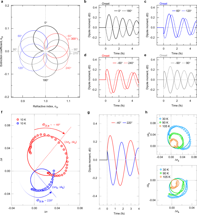
a n,k on the complex plane as a function of quantum interference-induced phase (ΦQI). The circular contour is rotated by the amount of ΦQI from the +y-axis. b–e Time-domain oscillation of the dipole moment (d)(t) for four sets of a pair of ΦQI whose sum is 180°. Vertical dashed line is the onset of the dipole oscillation. f Δn,Δk on the complex plane for FePS3 at 10 K (below TN). Dots are experimental data while circular lines are simulation results with a quantum interference model. Red color for the (a) direction and blue color for the (b) direction. The dashed lines indicate the tilting angle (namely, ΦQI) of the circular contour from the +y-axis for each (a) and (b) direction. g The time-domain oscillation of (d)(t) for FePS3 at 10 K. Red color for the (a) direction and blue color for the b direction. h Temperature independence of the constraint for quantum interference effect for the (a) direction (top panel) and the (b) direction (bottom panel).
In our experimental data, we observe the simultaneous onset of the dipole moment d(t). As depicted in Fig. 3f, the experimental Δn and Δk at 10 K (<TN) are plotted on the complex plane along with the consistent model fitting line. Specifically, the quantum interference-induced phase in the a direction is determined to be ΦQI,a = –40°, while in the b direction, it is ΦQI,b = 220°, resulting in the concurrent onset of two dipole oscillations in the a and b directions at time zero (Fig. 3g). For FePS3 below TN, ΦQI,a(b) is attributed to two quantum pathways in each a and b direction. Additionally, we observe that the dipole moments in both a and b directions satisfy the sum rule in k spectra of FePS3, where ΦQI,a + ΦQI,b = π [The missing area of k in the b direction is compensated by the increasing area of k in the a direction in Fig. 2]. This sum rule suggests a quantum mechanical entanglement between the anisotropic polarizations along the a and b directions. We note that the values of ΦQI,a(b) remain nearly constant up to temperatures below TN (Fig. 3 h). This reflects the nature of the correlation between two directional dipole moments under distinct quantum interference in the AFM semiconductor FePS3. Due to the alignment of spin (Ising type)25,30, the directional dipole moments in FePS3 are influenced by different quantum interferences, but they interact with each other to conserve the charge of the entire system.
We investigate the variation in quantum anisotropy with the thickness of FePS3 crystals to explore potential routes for controlling quantum interference and manipulating materials. Figure 4a illustrates the n and k spectra of three FePS3 crystals with different thicknesses (128 nm for S1, 156 nm for S2, and 431 nm for S3). At 125 K (above TN), where spin ordering is absent (left panels in Fig. 5a), the n and k values are relatively consistent among the three samples (S1–S3), showing their intrinsic nature without quantum interference effects (see Supplementary Fig. 8). However, below TN, the three samples exhibit differences in their n and k spectra. Particularly, at 10 K (below TN), where antiferromagnetic spin ordering is present, the n and k spectra exhibit variation among the three samples, despite the use of precise thickness for their acquisition from transmission spectra. We note that the spectral region exhibiting quantum interference displays an unconventional thickness-dependent variation in n and k values, while the region free from quantum interference shows a conventional thickness-independent behavior in n and k, ruling out any fault in the data acquisition. The individual FePS3 samples demonstrate anisotropic n and k spectra below TN, indicating the reproducibility of quantum anisotropy.

a The refractive index (n) and extinction coefficient (k) for three samples with different thicknesses (S1 with 128 nm, S2 with 156 nm, and S3 with 431 nm). Above TN (left panels), both n and k are nearly identical for three samples. However, below TN (right panels), the level of anisotropy depends on the sample thickness. b The d–d transition peaks exhibit nearly identical splitting for all three samples. The values of U–J and U + J are estimated from the peak (dip) positions in the Δk spectra in the (a) (b) direction below TN (inset: left panels for S1, middle for S2, right for S3). c Temperature-dependent linear birefringence (LB) and linear dichroism (LD) for three samples (left panels for S1, middle for S2, right for S3). d Δn, Δk on the complex plane for three samples at 10 K. Dots are experimental data, and circular lines are fitting results with our quantum interference model. Red color for the (a) direction and blue color for the (b) direction. The tilting angles (namely, ΦQI) of the circular contour are nearly identical for all the samples.

a (Left panel) Temperature independence of quantum interference-induced phase (ΦQI) for three samples. (Right panel) Thickness independence of ΦQI measured at 10 K for six samples. (Top panels) Below TN, the ΦQI value is represented by a rotation of the light-induced electronic polarization P on the complex plane. At U + J, the polarization in the (b) direction (Pb) is rotated by ΦQI,b = 220°. At U–J, the polarization in the (a) direction (Pa) is rotated by ΦQI,a = –40°. Here, we set the direction of the P vector from – to +. Above TN (paramagnetic phase), both Pa and Pb are degenerate, without pointing to a certain direction on the complex plane. Dots are experimental data and lines are guides to the eyes. The fitting error bar is extracted from the 95% confidence interval. b Phase transition of the dipole moments across TN. The light-induced PSSB,a and PSSB,b are obtained from the change in the dielectric constant ε1,a and ε2,b, according to the fact that P is proportional to ε. c Quantum anisotropy due to spontaneous symmetry breaking below TN. Below TN, the system is described by Mexican hat potential where the energy minima are infinitely degenerate along the circular rim, distinct from the conventional parabolic potential above TN. For FePS3 below TN, the order parameter-like PSSB is spontaneously pointing at ΦQI,a = –40° for the (a) direction (bottom left panel) while no preferred angle of P at the center of the potential (bottom right panel) above TN.
The results reveal that the peak positions in the a and b directions are nearly the same for the three samples with different thicknesses (Fig. 4b), showing that the peak splitting accompanied by spin ordering (i.e., exchange coupling J) is not affected by the thickness effect. The thickness-dependent n, k spectra (Fig. 4a) suggest differences in quantum anisotropy among the three samples. In Fig. 4c, the LB and LD spectra for the three samples are presented, with maximal LB values of ~0.075 (Sample S1), 0.10 (S2), and 0.125 (S3) and with maximal LD values of 0.075 (S1), 0.10 (S2), and 0.125 (S3), increasing with thickness at 10 K. One notable observation is that the broadening of the d–d transition peak20 is smaller for thicker samples.
Then, what happens in the circular contour of Δn and Δk? As presented in Fig. 4d, the circle size increases for thicker samples, consistent with the smaller broadening observed in thicker samples. Interestingly, however, the tilting angle corresponding to ΦQI is nearly identical for all three different samples. In other words, the onset of their dipole moments is identical regardless of the thickness difference of the FePS3 crystals. Their consistent ΦQI values imply that the thickness-dependent LB and LD are not directly attributed to quantum interference only.
We note that the observation of thickness-dependent n and k values is an unconventional result, because n, k are typically not considered as bulk properties (i.e., thickness-independent properties). First, we emphasize that we have accurately measured the thickness of each sample and used these values in our calculations of n and k. The thickness-dependent behavior of n and k observed in the quantum interference regime is not due to errors in thickness normalization. This is supported by the consistent n and k values observed above TN for all samples (Fig. 4a) regardless of thickness, and by the consistent n and k values even below TN in the spectral region where quantum interference is absent (see Supplementary Fig. 9). Our results demonstrate that the thickness-dependent behavior of n and k is specific to the spectral region where quantum interference occurs. Second, we rule out the cavity effect in vdW semiconductors21. Due to their high transparency, incident light travels through the sample via multiple internal reflections, resembling a cavity (see Supplementary Fig. 10). Here, despite thickness variations, all samples allow for only direct and single round-trip (when N = 1) transmissions of light. In other words, the n, k spectra considered only direct and single round-trip (when N = 1) are nearly identical to those considered infinite round-trip. This indicates that the cavity effect is unrelated to the thickness-dependent quantum anisotropy.
We propose a more realistic explanation for the thickness-dependent n and k values in the quantum interference regime: a synergy between quantum interference and sample thickness. The exotic thickness proportionality of quantum anisotropy may come from the intrinsic quantum interference effect. The magnitude of these effects is directly proportional to the number of dipole moments (i.e., polarizations) involved in the interference process, which scales with sample thickness. Our analysis indicates that the emerging anisotropic polarization below TN exhibits a similar thickness proportionality, clarifying the relationship between quantum interference and quantum anisotropy (see Supplementary Fig. 11). In contrast, the ΦQI is a thickness-independent intrinsic property, as confirmed by our experiments (Fig. 5a). Such quantum anisotropy is distinct from both intrinsic classical anisotropy and extrinsic effects like multiple internal reflections, which can be mitigated by varying the sample thickness. The thickness dependence of quantum anisotropy offers an intriguing opportunity to engineer and control the strength of quantum interference effects, enabling the exploration of new phases of matter, from bulk to thin limits.
Discussion
What is the physical significance of quantum anisotropy, particularly in the context of spontaneous symmetry breaking and quantum phase transitions? We explore this concept by considering the dipole moment of FePS3 associated with the d–d transition20,26,27,28. Above TN, where quantum interference is absent, the dipole moment P is isotropic, resulting in isotropic absorption (as depicted in the top panels of Fig. 5a). However, below TN, quantum interference alters the electronic polarization to P∙exp(iΦQI), rotated by the amount ΦQI on the complex plane. This rotation is directional in FePS3: PSSB,a in the a direction rotates by ΦQI,a = –40°, while PSSB,b in the b direction rotates by ΦQI,b = 220° (the top panels of Fig. 5a). We mention that this rotation is consistent across samples of different thickness. The preference of a certain angle for P under quantum interference is akin to U(1) symmetry breaking, which is similarly observed in superconductivity31,32.
As shown in Fig. 5b, the P in each direction shows a clear phase transition across TN. Also, the quantity P∙exp(iΦ) resembles the superconducting order parameter ψ = |ψ| *exp(iθ), where |ψ| is a square root of the super-electron density and θ is a phase factor related to the supercurrent flow33. Above TN, the isotropic P resides at the minimum (center) of the parabolic potential, as depicted in Fig. 5c. Conversely, below TN, P shifts away from the center to reach a new minimum of the Mexican hat potential through spontaneous symmetry breaking at a given ΦQI. This break in symmetry selects one of the infinitely degenerate minima encircling the Mexican hat (or Higgs) potential31,32. This viewpoint offers novel insights into spontaneous symmetry breaking and the quantum phase transition of FePS3 via quantum interference. Like correlated AFM FePS3, in other molecular or solid-state systems governed by the orbital physics, light excitation enables the control of orbital occupancy and therefore the electronic polarization P, and the quantum interference between degrees of freedom results in the spontaneous symmetry breaking with P·exp(ΦQI), allowing for quantum chemistry for the material metamorphosis by light. Understanding this physics could provide insights into longstanding puzzles in symmetry breaking phenomena such as superconductivity, magnetism, and Higgs physics.
Methods
Sample preparation
Quartz substrates (iNexus, INC.) were prepared to a size of 0.5 cm ⨯ 0.5 cm. To eliminate unwanted organic residues, the substrates underwent sonication in acetone. FePS3 flakes (2D Semiconductors) were then transferred onto the quartz substrate via mechanical exfoliation. The thickness of the transferred FePS3 flakes was verified using atomic force microscopy (AFM, Park Systems, INC.). To avoid oxidation or aging, all transfer procedures were conducted inside a glovebox with H2 O and O2 below 1 ppm.
Confocal microscope absorption spectroscopy
Temperature-dependent optical spectroscopy was conducted within an optical cryostat (Montana Instruments). A broadband white light source (OSL2IR, Thorlabs) over the spectral range of 480–4000 nm, coupled with a linear polarizer (WP25M-UB, Thorlabs) of an extinction ratio greater than 8000:1 is used. In our confocal spectroscopy configuration, a multi-mode fiber with a 50 μm core size channeled the light into a CCD spectrometer (CCS200, Thorlabs), which covers a spectral range of 200–1000 nm. This setup, combined with a 10× objective lens (M Plan Apo NIR, Mitutoyo) featuring a numerical aperture (NA) of 0.26, enabled the acquisition of optical spectra across 480–1000 nm with a focused sample area diameter of 5 μm.
Acquisition of n, k
Method I (Main text): Low-k approximation
When light passes through a flake of FePS3 exfoliated on a substrate, the transmission spectrum is described by normalizing the total transmission of the film-substrate system to that of the bare substrate. Using the transfer matrix method34,35, the transmission ({{{rm{T}}}}_{{{rm{FeP}}}{{{rm{S}}}}_{3}}) of the FePS3 thin film is expressed as:
Here, ({n}_{1}=1) is the refractive index of vacuum, ({n}_{2}=n+{ik}) is the complex refractive index of FePS3, ({n}_{3}) is the refractive index of substrate (here, ({n}_{3}approx 1.54) for quartz), d is the thickness of the FePS3 film, and λ is the wavelength of the incident light. This equation considers multiple reflections and interference effects within the FePS3 thin film system and serves as the foundation for determining n and k.
To determine the complex refractive index ((n) and (k)) of FePS3, we utilize the approximation that the refractive index (n) is significantly larger than the extinction coefficient (k) ((ngg k)) generally in semiconductors. Below is the step-by-step procedure to obtain (n) and (k).
Step I. Initial Assumption
The complex refractive index of FePS3 is given as ({n}_{2}=n+{ik}). For the initial iteration, we assume (n={n}_{0}), where ({n}_{0}approx 2.69) is an approximate constant value compatible with our various FePS3 samples. Additionally, we set (kapprox 0) for simplicity. However, we retain (k) within the exponential terms, such (exp left(-4pi {kd}/lambda right)), because even a small value of (k) significantly affects the attenuation factor due to its exponential nature. This approach simplifies the first iteration while preserving the mathematical framework needed for accurate updates in subsequent iterations.
Step II. Definition of (widetilde{A}) and (widetilde{B})
Using the ({n}_{2}), we define the parameters (widetilde{A}) and (widetilde{B}), which account for multiple reflections and interference effects in the FePS3 thin film system:
During the first iteration, ({n}_{2}={n}_{0}) simplifies both (widetilde{A}) and (widetilde{B}) to real values, reducing calculation complexity.
Step III. Quadratic equation for (k)
The transmission equation Eq. (1) ({{{rm{T}}}}_{{{rm{FeP}}}{{{rm{S}}}}_{3}}) can be expanded into a quadratic equation in terms of (xequiv exp left(-4pi {kd}/lambda right)):
where the coefficients are expressed as:
Solving for (x) gives (k) as:
Step IV. Iterative refinement
Once (k) is calculated, the refractive index (n) is updated using the Kramers-Kronig relation:
where ({n}_{0}) is the initial approximation, and ({{mathscr{P}}}) represents the Cauchy principal value over the spectral range [({omega }_{1}), ({omega }_{2})]. Updated (n) and (k) redefine ({n}_{2}=n+{ik}), making (widetilde{A}) and (widetilde{B}) complex for subsequent iterations. This process is repeated at least five times to ensure convergence.
Method II (Supplementary, for comparison with Method I): optical constant model fitting
The transmission intensity of both the FePS3 sample and the quartz substrate was measured, alongside a background signal obtained by blocking the light source. This allowed us to calculate the specific transmission for FePS3 as T = (TFePS3+Substrate − Tbackground)/(TSubstrate − Tbackground), from which the absorbance spectra were derived using the relation A = −ln(T). To further decipher the real and imaginary parts of the optical constants, we applied a modeled transfer function—incorporating six Gaussian and one Cauchy model—to the experimental transmission data (above TN).
I) Gaussian model36:
where A is resonance amplitude, E0 is resonance frequency, σ is broadening parameter equal to full-width-half-maximum, and D stands for Dawson function (Dleft(xright)=exp left(-{x}^{2}right),{int }_{0}^{x}exp left({t}^{2}right){dt},).
II) Cauchy model35:
where (lambda) is the wavelength of light, the constants from AC to EC are the dispersion parameter.
Quantum interference model
To analyze the quantum interference effect, we used the dielectric constant model as below (not a typical Lorentz model but a Lorentz model multiplied by a phase factor):
where ωp is the oscillator strength, ω0 is the center frequency, γ is the broadening factor, and ΦQI is the quantum interference-induced phase.

Responses