Adiabatic leaky integrate and fire neurons with refractory period for ultra low energy neuromorphic computing

Introduction
Computers designed according to the von Neumann separation between processing and memory, tightly synchronized by clock signals and based on a high-precision digital representation have not been conceived for the complex cognitive tasks and the extreme energy efficiency required by edge artificial intelligence (AI) applications. In-memory-computing has thus emerged as a compelling paradigm to improve energy efficiency in hardware solutions dedicated to AI. Moreover, neuromorphic computing is being actively explored as a bio-inspired approach to information processing that is based on spiking neural networks1, and is capable of sophisticated tasks including real-world sensory processing2. The essential components of neuromorphic hardware are artificial synapses and neurons (see Fig. 1), with artificial synapses being pivotal also for crossbar arrays employed in accelerators for neural network inference3,4,5.

a Sketch of an artificial spiking neuron in a spiking Hopfield neural network with self-recursion. The input spikes are weighted by the synapses and then integrated into the membrane potential, which finally fires an output spike upon reaching an appropriate threshold. b Non-adiabatic driving of a capacitor by an abrupt input voltage VIN having practically null rise and fall times (T = 0). The dissipation during each charging or discharging is (frac{1}{2}C{{V}_{DD}}^{2}) and does not depend on R. c Adiabatic driving of a capacitor by a VIN waveform with rise and fall times (T) sufficiently longer than the time constant τ = RC of the circuit. In this case, the conduction losses become proportional to τ/T and so can be arbitrarily reduced by slowing down the driving signal. Since in the charging-discharging cycle only a fraction of the supplied energy is dissipated on R, during the discharging the power supply can recover a significant fraction of the supplied energy.
Many implementations of artificial synapses have been proposed including CMOS sub-threshold circuits6,7,8,9, switched capacitors10, oxide-RAM11, and Li-ion transistors12. Moreover, in order to reduce the area and improve the energy efficiency, single-device synapses have been explored using diverse kinds of memristors13,14,15.
Capacitive synapses can enable a highly energy efficient, charge domain in-memory-computing16,17,18, and non-volatile tunable capacitors, or memcapacitors, could provide an ideal platform for such an implementation19,20,21,22. In fact, in contrast to memristors, the read-out of capacitive synapses is not inherently dissipative23,24. Nevertheless, the usual operation of capacitors, sketched in Fig. 1b, implies the dissipation in the driving circuitry of an energy comparable to the energy stored in the capacitor itself.
Thus, in the quest for a further leap forward in the energy efficiency of neuromorphic hardware and in-memory-computing, the adiabatic operation of the capacitors seems very attractive22,25.
The adiabatic operation illustrated by Fig. 1c has already been explored for logic circuits, but without reaching a significant impact. This was due to the challenges in the design of logic gates and of multi-phase power-clock generators, to the penalty in dynamic performance26, as well as to the fact that the adiabatic operation can effectively suppress the dynamic energy but not as much the static leakage energy, whose impact has become comparatively more important with the scaling of CMOS technologies and at low operating frequencies.
The adiabatic operation can be much more rewarding in neuromorphic circuits employing capacitive synapses22,25, because these bio-inspired circuits inherently target a relatively low-frequency operation and, moreover, the dynamic energy consumption tends to dominate the static dissipation due to the use of quite large capacitors.
In this paper, we expand on our previous work in ref. 27 by presenting, for the first time to our knowledge, an adiabatic Leaky Integrate-and-Fire neuron featuring an accumulation of the incoming input spikes, an exponential leakage of the membrane potential and a tunable refractory period. We report transistor-level simulations, carried out with the commercially available XP018-180 nm XFAB CMOS technology, demonstrating that our design is able to recover the charge supplied to the capacitive synapses and soma with minimal losses, in fact the circuit can reach an energy efficiency higher than 99% for the slowest resonance frequencies. Our results reveal a minimum energy per synaptic operation of 470 fJ at a 500 kHz resonance frequency with a supply voltage VDD = 1.8 V. Such an energy per synaptic operation translates into a 9× energy saving with respect to a non-adiabatic operation.
Results
The adiabatic architecture proposed in this work is shown in Fig. 2. The core of our circuit is a crossbar array of synapses which natively implements a spiking Hopfield network with self-recursion (see Fig. 2b). Nonetheless, any other network architecture can be obtained by pruning the undesired network connections, namely by setting their corresponding synaptic weight to zero. The spikes are distributed through the network based on the Address-Event Representation (AER) protocol28. In particular, both the word-lines (WL) and the neurons on the bit-lines (BL) are identified by matching identifiers, so that the spikes fired by the i-th neuron can be forwarded to all neurons through the synapses of the i-th word-line.
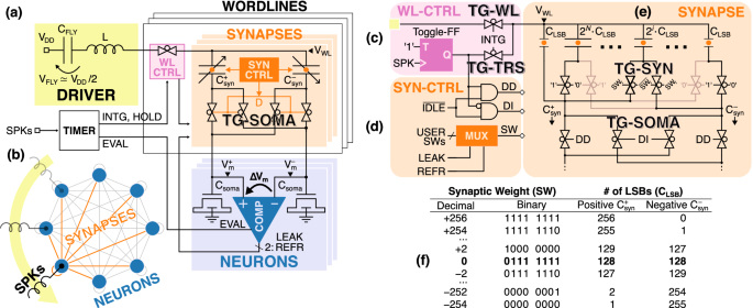
a Global architecture featuring an inductive driver (yellow) that resonates with the word-line capacitance selected by its WL controller (pink). Each word-line comprises a row of differential synapses (orange) that weigh and forward the spikes to the soma of the neurons on the bit-lines (blue), where they are integrated into the differential membrane potential (ΔVm), that is finally monitored by a comparator. b Time-multiplexing of a single driver among all the neurons of the Hopfield network. c Details of the WL controller. d Synapse controller which manipulates the internal configuration of the synapse based on the leakage and refractory period of the corresponding neuron. e Binary-encoded capacitor bank that implements the differential capacitive synapse. f Encoding of the synaptic weight and corresponding number of Least Significant Bit (LSB) capacitors that form the positive and negative synaptic capacitors (({C}_{syn}^{pm })).
In our architecture, all the energy involved in the neuromorphic computation is supplied to the neurons and synapses in an adiabatic fashion, thus greatly reducing the conduction losses in the circuit. More details about the operation of the system will be presented in the “Discussion” section. In brief, upon each input spike, an inductive driver (yellow) resonates with the target capacitive word-line, which consists of differential capacitive synapses (orange) that form two capacitive dividers with the differential soma of the neurons (blue). Thanks to the resonance, the driver can adiabatically transfer or recover energy to and from the word-lines. The supplied current is weighted by the synapses and then integrated by the soma into the differential membrane potential (ΔVm) as a function of their synaptic weight (SW). Finally, the membrane potential is monitored by the neuron comparator, which fires an output spike upon the crossing of a certain threshold.
One specific novelty of our design is its capability to make use of both the adiabatic charging and recovery phases to accumulate the incoming spikes in the membrane potential of the neurons. Following the same working principle, a synchronous spiking clock (CLK) provides the neurons with an adiabatic time-base, which is used to induce discrete inhibitions of the membrane potential, so as to achieve an adiabatic implementation of the leakage and refractory period of the neurons.
Figure 3 shows an example of the overall computation. The train of spikes from the neurons (black SPK) and clock spikes (gray CLK) in Fig. 3a are forwarded to the neurons through four different synaptic weights (SW), resulting in different behaviors of their membrane potential, which are reported in Fig. 3c–f. In particular, each input SPK increases the membrane potential proportionally to the excitatory SW, and then the membrane potential exponentially decays towards the resting state due to the CLK-driven leakage of the neuron. Furthermore, whenever the membrane potential overcomes the spiking threshold set by the comparator (dashed lines), the neurons fire the output spikes of Fig. 3b and then enter a refractory period. The black triangles show how the circuit can adjust the duration of the refractory period of the neurons, which are also reported in the figure. As a reference, the pink neuron having the highest SW as well as the shortest refractory period exhibits the most lively spiking activity.
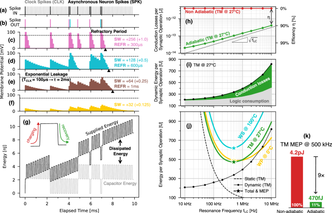
Example of the neuromorphic computation. a Synchronous clock spikes (CLK, gray) that provide a time base for both the neuron leakage and refractory period, and asynchronous spikes (SPK, black) weighted by the synaptic weights. b Output spikes fired by the neurons in (c) to (f) for different synaptic weights (SW) and duration of the refractory period (REFR). All neurons share the same time constant for the exponential leakage. g Time evolution of the energy supplied to the circuit (black) and stored in the capacitors (gray), whose difference provides the dissipated energy. Energy performance simulated from the example on the left and expressed in terms of Energy per Synaptic Operation. h Adiabatic conduction losses (green line) versus the resonance frequency fLC and corresponding adiabatic efficiency (right y-axis), defined as the saving with respect to the non-adiabatic energy dissipation (red line). i Dynamic energy per synaptic operation comprising the conduction losses (green) and the consumption of the logic (gray) plotted versus fLC. j Total ESOP extracted at the Typical Mean at 27 °C (TM, green), Worst Power at 0 °C (WP, yellow) and Worst Speed at 100 °C (WS, cyan) corners including both the dynamic and static energy contributions (reported for TM corner only). The opposite fLC dependence of the dynamic and static energies results in a Minimum Energy Point (MEP, colored stars) at fLC = 500 kHz for all corners and corresponding to 470 fJ for the TM corner. k Comparison between the nominal (TM @ 27 °C) adiabatic MEP at fLC = 500 kHz and the corresponding energy in nominal non-adiabatic mode.
Below, Fig. 3g reports the energy supplied to the circuit over time (black), as well as the total energy stored in all its internal capacitors (gray). Since the energy remaining in the synapses and neurons plays an active role in the computation, the actual dissipated energy is evaluated as the difference between the supplied and said stored energy.
The simulations on the left side of Fig. 3 were repeated for many different resonance frequencies fLC. The resulting energy performance are analyzed as a function of fLC in the right side of Fig. 3, where they are expressed in terms of Energy per Synaptic Operation (ESOP), namely normalized to the number of spikes (including clock spikes), and to the number of synapses served by each WL.
First, the left y-axis of Fig. 3h reports the total conduction losses, which correspond to the adiabatic driving efficiency on the right y-axis. Such efficiency is here defined as the difference between the conduction losses resulting from our adiabatic operation (green), and the non-adiabatic upper limit (frac{1}{2}{C}_{WL}{{V}_{DD}}^{2}) obtained by operating our circuit in a completely non-adiabatic mode (red line). A distinctive feature of adiabatic systems is the systematic reduction of the conduction losses for decreasing fLC29. As can be seen, our design results in conduction losses roughly proportional to the square root of fLC, consistently with the frequency-dependent optimization of the transmission gates discussed in “Methods” and in Supplementary Note 4. Thanks to such a frequency scaling, our adiabatic efficiency remains higher than 90% over the whole explored frequency range and even exceeds a 99% efficiency at the lowest resonance frequencies.
In Fig. 3i it is shown the dynamic ESOP, which comprises the conduction losses of Fig. 3h (green), as well as the energy consumed by the auxiliary logic (gray). The Dynamic ESOP mirrors the scaling of the conduction losses at relatively high frequencies, while it deviates at the lower frequencies as the consumption of the logic circuits becomes progressively dominant with respect to the adiabatic conduction losses.
In adiabatic systems operating at low frequencies, the static dissipation may become the dominant source of energy consumption. As such, the static power of each sub-circuit has been thoroughly evaluated for each corner, and it is reported in Supplementary Note 4 for the TM corner at 27 °C only.
Figure 3j reports the total ESOPs of all the design corners (colored solid lines), obtained by adding the dynamic energy of Fig. 3i to the static energy estimated for the full crossbar; the corners TM, WS, WP are defined and described in the “Simulation Framework” paragraph of the “Methods” section. The isolated dynamic (black dotted line) and static energy (black dashed line) are also shown in Fig. 3j, but only for the TM corner at 27 °C. The opposite frequency scaling of the static and dynamic energy leads to a Minimum Energy Point (MEP, colored stars) at a resonance frequency of about 500 kHz for all corners.
In particular, thanks to the high adiabatic efficiency reached by both the TM at 27 °C (green) and WP at 0 °C (yellow) corners, their MEPs result as low as 470 fJ and 490 fJ, respectively. On the other hand, for the WS corner at 100 °C (cyan) the MEP increases to 620 fJ, due to both higher conduction losses (owing to a higher resistance of the transmission gates) and higher static consumption (due to a degradation of the MOSFETs off-current at the high operating temperature).
As summarized in Fig. 3k, the nominal MEP yields a 9× energy saving compared to an identical circuit operated in a completely non-adiabatic mode. The detailed energy breakdown of the nominal adiabatic and non-adiabatic benchmarks can be found in Supplementary Note 5.
In Table 1, we compare the performance of our adiabatic LIF neurons with previously published neuromorphic circuits, including digital implementations30,31, mixed-signal subthreshold options8,9, and adiabatic circuits25. Mixed-signal systems tend to reach an energy efficiency higher than digital solutions, albeit at the cost of a lower configurability. Compared to the adiabatic perceptron in ref. 25, this work has both introduced novel functional aspects and achieved a lower overall ESOP. Indeed, our results suggest that the adiabatic operation is a promising option to further improve the energy-efficiency of neuromorphic circuits.
Discussion
Adiabatic resonance-driven charge recovery
The inductive driver (yellow in Fig. 2a) is tasked to transfer the energy back and forth between the power supply (VDD) and the target WL of the crossbar. In particular, the driver consists of an inductor L and a large flying capacitor CFLY, which is pre-charged at VDD/2 and should always preserve such a voltage. The operation of the driver is demonstrated in Fig. 4. The arrival of each input spike (Fig. 4a) starts the adiabatic integration phase (INTG, Fig. 4b), where the selected WL controller enables a transmission gate (TG-WL, see Fig. 2b) to connect the driver to the word-line. This triggers the resonance between the inductance L and the series of CFLY and the WL capacitance CWL. Such resonance is crucial to convert any abrupt voltage step across the inductor to an adiabatic-compatible voltage swing that drives the WL capacitance. In particular, if the WL voltage begins at GND/VDD, the connection with the driver causes a positive/negative VDD/2 voltage drop across the inductor. In turn, this triggers the rising/falling sinusoidal swing of the word-line voltage shown in Fig. 4c, which can be expressed as:
with upper and lower sign applying respectively to falling and rising. The charging/discharging of the WL is driven by the positive/negative sinusoidal current reported in Fig. 4d, which can be written as:
where t0 is the spike arrival instant, fLC the resonance frequency and IL,pk = πCWLVDDfLC is the peak amplitude of the current oscillation. Upper and lower signs in Eqs. (1) and (2) correspond to a VWL waveform starting at GND or VDD, respectively.
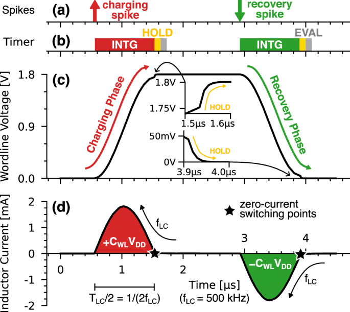
a Asynchronous input spikes that trigger either a charging or a recovery phase. b adiabatic integration phase (INTG) followed by a HOLD phase that corrects the incomplete transition of the word-line before the comparator evaluates the membrane potential (EVAL). c Word-line voltage which is alternatively charged (red) and discharged (green) at any subsequent spike. The insets show the correction during the HOLD phase. d Sinusoidal current waveform that transfers a charge CWLVDD back and forth between the supply and the WL upon each spike. The zero-current switching points are marked with a black star.
Without any external intervention, the resonance would continue to shuttle energy from the power supply to the WL during the upswing (charging phase in red), and recover that same energy back during the downswing (recovery phase in green). All the resistive elements on the path of the current would however damp such oscillation by dissipating energy via Joule heating.
In our architecture, however, the timer forces the WL controller to disable the TG-WL and so interrupt the INTG phase after a single half-period TLC/2, namely when the word-line nominally completes the charge to VDD (charging phase) or the discharge to GND (recovery phase). Such a timing ensures the zero-current switching of the TG-WL, which is a well-known requirement for achieving an adiabatic operation because it minimizes the losses when turning off the transistors32.
As it can be seen in Fig. 4, the input spikes trigger INTG phases that alternatively start with either a completely charged or discharged word-line. This behavior ensures the seamless alternation of charging and recovery phases despite the identical control signals. For clarity, we will denote the spikes that trigger a charging phase as charging spikes, and those triggering a recovery phase as recovery spikes.
After any INTG, the word-line is kept in HOLD (yellow of Fig. 4b) until the next INTG. While in HOLD, the tristate of the WL controller takes control of the word-line by enforcing and then maintaining either VDD (after a charging phase) or GND (after a recovery phase). As shown in Fig. 2b, such tristate consists of a Toggle Flip-Flop (T-FF), which inverts its output upon each input spike thus mirroring the transitions of the word-line, and then a transmission gate (TG-TRS) that disconnects T-FF during the adiabatic integration. Before the evaluation by the comparator (EVAL, gray in Fig. 4b), the HOLD phase corrects any incomplete charging or discharging of the word-line, as shown in the insets of Fig. 4c. In doing so, both the T-FF and the TG-TRS produce non-adiabatic conduction losses which, as such, depend only on the amplitude of the correction required by the WL voltage but not on the sizing of the transistors.
Capacitive synapses and soma
Our architecture employs differential capacitive synapses realized with the binary-encoded capacitor bank sketched in Fig. 2e, which gets split by a digital encoding of the Synaptic Weight (SW) in two differential synaptic capacitors, ({C}_{syn}^{+}) and ({C}_{syn}^{-}). In particular, depending on the i-th bit of the synaptic weight (SWi), a row of transmission gates (TG-SYN) connect the i-th capacitor (Csyn,i) either to the left branch to make up the positive synaptic capacitor (SWi = 1), or to the right to be part of the negative one (SWi = 0).
Such differential structure serves two interlinked purposes. First, it represents the synaptic weight in the difference between the two synaptic capacitors (i.e., (SWpropto ({C}_{syn}^{+}-{C}_{syn}^{-}))), which can be either positive for an excitatory synapse (({C}_{syn}^{+}, > ,{C}_{syn}^{-})), negative for an inhibitory synapse (({C}_{syn}^{+}, < ,{C}_{syn}^{-})), or null (({C}_{syn}^{+}={C}_{syn}^{-})). Second, it results in a total synaptic capacitance ({C}_{syn}=({C}_{syn}^{+}+{C}_{syn}^{-})) independent of the synaptic weight, thus ensuring a good tracking of the resonance irrespectively of the synaptic weight and without resorting to a large equalizing capacitor25. In the table of Fig. 2f are reported the attainable values of the synaptic weight, together with their digital encoding and their corresponding ({C}_{syn}^{+}) and ({C}_{syn}^{-}) capacitances expressed in terms of number of Least Significant Bits (LSB). More details on the variability of the capacitor bank and on the linearity of the resulting transfer function can be found in Supplementary Note 1.
Below the synapses, there is another row of transmission gates (TG-SOMA, see Fig. 2a, e) that connect each synaptic capacitor to one of the two identical capacitors Csoma that form the differential soma that acts as the bit-line shared by all WLs. The differential membrane potential ΔVm between the Csoma capacitors represents the neuron membrane potential that is finally monitored by the neuron comparator, which is described in Supplementary Note 2.
As it will be detailed in the following sections, each synapse is controlled by a synapse controller (SYN-CTRL, see Fig. 2d), which dynamically manipulates all the TG-SYNs and TG-SOMAs depending on the state of the neuron and word-line, respectively. In particular, the SYN-CTRL can dynamically set the SW to zero to ignore the incoming spikes (e.g., during the refractory period), or restore it to its user-defined value. As for the TG-SOMAs, they select which synapse ({C}_{syn}^{pm }) is connected to each node ({V}_{m}^{pm }). Moreover, the TG-SOMAs can also be disabled to put the word-line in IDLE and enable the multiplexing of the external inductor among multiple WLs (Fig. 2b).
Accumulation of charging and recovery spikes
In previous literature, the resonant adiabatic driving was successfully employed to compute Multiply-and-Accumulate (MAC) operations25,33. As sketched in Fig. 5a, in those designs the charge is adiabatically provided during an initial charging phase as the input to each branch of the WL (xi). Such inputs are then weighted by capacitive synapses (wi) and accumulated into the terminal somas shared by multiple WLs, whose voltage is finally interpreted as the result of the MAC operation (∑iwixi). Immediately afterward, the charge is recovered by adiabatically discharging the synapse-soma capacitive dividers. As a consequence, each recovery phase cancels out the effect of the previous charging phase, thus making each MAC operation independent of the previous ones.
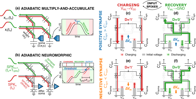
a Sketch of an adiabatic multiply-and-accumulation operation (MAC). The charge is first supplied adiabatically (red), then adiabatically recovered (green) after sampling the outcome of the MAC (blue), thus resetting the state of the integrating capacitor. b Sketch of an adiabatic neuromorphic operation, whereby an alternation of charge (red) and recovery (green) spikes are accumulated into the membrane potential of the soma. Synapse-soma capacitive dividers controlled by the signal D during the charging (red) and recovery phase (green) for either a positive synaptic weight (({C}_{syn}^{+} ,> ,{C}_{syn}^{-}), c, d in blue) or a negative synaptic weight (({C}_{syn}^{+}, < ,{C}_{syn}^{-}), e, f in orange). In (c) and (e), the larger synapse results in a greater charging of the Csoma connected respectively at ({V}_{m}^{+}) and ({V}_{m}^{-}), thus increasing and reducing ΔVm, respectively. Conversely, in (d) and (f), the larger synapse results in a greater discharging of the Csoma connected respectively at ({V}_{m}^{-}) and ({V}_{m}^{+}), again increasing and reducing ΔVm.
However, in order to implement the functionalities required by a spiking neural network, the results of many MAC operations need to be accumulated into the soma along successive computation cycles. To this purpose, in our architecture, the charging and the recovery phases have a cumulative effect on the membrane potential of the neurons, as sketched in Fig. 5b, which is crucial to compute a valuable MAC operation during both adiabatic phases. In particular, the recovery phase accomplishes both a computational task by modifying the membrane potential, and an electrical one by enabling the adiabatic recovery of the charge transferred and then stored in the WL by the previous charging phase.
The accumulation of the input spikes is achieved thanks to a proper reconfiguration of the differential structure of both the synapses and neurons. The ({C}_{syn}^{+}), ({C}_{syn}^{-}) can be connected either at ({V}_{m}^{+}) or ({V}_{m}^{-}) to form two capacitive dividers that govern the charge induced to the corresponding Csoma. In particular, the larger synaptic capacitor will induce a larger charge variation δQsoma in the connected Csoma as dictated by:
where the upper and lower signs correspond to the Csoma connected to respectively ({C}_{syn}^{+}) and ({C}_{syn}^{-}), while ΔVWL is the voltage swing at the word-line induced by the input spike, namely ΔVWL = +VDD for a charging spike and ΔVWL = −VDD for a recovery spike (see Fig. 4c).
The resulting charges in the two Csoma capacitors give rise to two single-ended potentials ({V}_{m}^{pm }) and thus to a differential voltage (Delta {V}_{m}=({V}_{m}^{+}-{V}_{m}^{-})) that represents the neuron membrane potential.
In order to accumulate the effects produced by many δQsoma on the differential membrane potential, the SYN-CTRL inverts the capacitive dividers by properly controlling the TG-SOMAs through the signal D. More specifically, the following configurations are possible: (1) direct divider used during charging spikes (D = 1, ({C}_{syn}^{+}) connected to ({V}_{m}^{+}) and ({C}_{syn}^{-}) connected to ({V}_{m}^{-})); (2) inverted divider used during recovery spikes (D = 0, ({C}_{syn}^{+}) connected to ({V}_{m}^{-}) and ({C}_{syn}^{-}) connected to ({V}_{m}^{+})); (3) IDLE mode, where D is bypassed to disable all TG-SOMAs and thus disconnect the WL. This latter configuration makes it possible to multiplex the inductor among multiple WLs.
Figure 5c,d illustrate an example for a positive synaptic weight (obtained by setting ({C}_{syn}^{+}, > ,{C}_{syn}^{-})), where the direct divider makes each charging spike charge the positive soma more than the negative one, thus increasing their differential membrane potential. Conversely, the inverted divider makes each recovery spike discharge the negative soma more than the positive one, which increases again the differential membrane potential, thus accumulating its contribution to the charging spikes. Figure 5e, f illustrate such behavior also for a negative synaptic weight (namely for ({C}_{syn}^{+} ,< ,{C}_{syn}^{-})).
By doing so, every spike yields a change δVm of the differential membrane potential equal to:
If we let sw = SW/2Nbit be the signed synaptic weight SW normalized between −1 and +1, and recall the Csyn definition ({C}_{syn}=({C}_{syn}^{+}+{C}_{syn}^{-})), the synaptic capacitances can be expressed in terms of sw as ({C}_{syn}^{pm }={C}_{syn}(1pm sw)/2) and substituted in Eq. (4) to obtain:
where c = Csyn/(2Csoma). We reiterate that, for a given synaptic weight, δVm is the same for both charging and recovery spikes.
Finally, by neglecting the neuron leakage that will be discussed in the following sections, we can estimate as NSPK = Vth/δVm the number of successive excitatory spikes necessary for a neuron to cross the threshold Vth of the comparator starting from the resting state at ΔVm = 0.
Spiking clock as adiabatic time reference
In biology, it is observed that the membrane potential of the neurons decays exponentially towards its resting potential due to the leakage of ions through the neuron membrane34. In complex SNNs, the inclusion of this leakage mechanism into a Leaky Integrate-and-Fire model (LIF, see Fig. 6a) enables the neurons to process temporally structured stimuli that carry relevant information also through the arrival times of the spikes35. This is the case for many edge applications such as real-time keyword spotting, health monitoring and gesture recognition36,37,38. Indeed, for this kind of tasks, it has been extensively demonstrated that the LIF model performs remarkably better than the simpler Integrate-and-Fire (IF) model, particularly in terms of an increased noise-robustness, better generalization capabilities and higher network accuracy39,40.
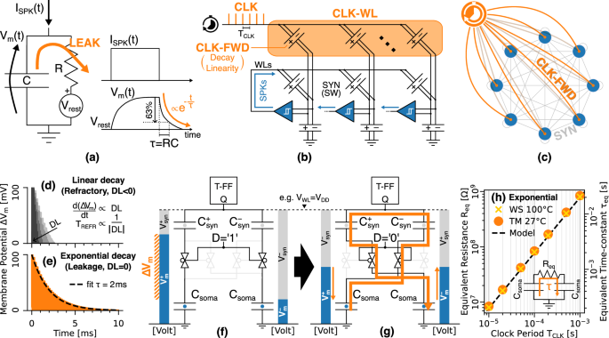
a Leaky-Integrate-and-Fire (LIF) neuron model. b Distribution of the clock spikes (CLK) to the neurons. The Clock Forwarders (CLK-FWD) of a dedicated Clock Word-line (CLK-WL) are electrically analogous to inhibitory synapses. c Network-level interpretation of the spiking clock. d, e Time decay of the membrane potential for TCLK = 100 μs, whose linearity is set by the decay linearity factor (DL) of the CLK-FWD: d linear decays obtained with increasingly negative DLs and exploited for the neuron refractory period. e exponential decay achieved with null DL and used to implement the neuron leakage; f, g Inversion of the capacitive dividers and corresponding charge sharing in the capacitors network (orange). h Resistance (Req, left y-axis) and exponential time constant (τeq, right y-axis) of the equivalent RC circuit in the inset, as a function of the clock period. The simulations of the exponential decay at the Typical Mean at 27 °C (TM, orange circles) and Worst Speed at 100 °C (WS, yellow crosses) corners agree with the model of Eq. (6) (dashed), and demonstrate the insensitivity to the operating temperature. Biologically plausible time constants in the order of the ms can be achieved with TCLK in the range of hundreds of μs.
In neuromorphic circuits, the leakage of the membrane potential is typically realized with a resistance R that discharges the soma C with an exponential time decay and a time constant τ = RC, as illustrated in Fig. 6a. In bio-inspired architectures that target both low-energy and biologically plausible time-scales, the required high effective resistance is typically realized with FETs working in the sub-threshold region9,41. Such implementations, however, are inherently dissipative and not compatible with our adiabatic approach.
For this reason, in our architecture, we devised an adiabatic implementation of the leakage, which makes use of the inductor to gradually decrease the membrane potential via adiabatic steps.
As it is depicted in Fig. 6b, a time reference is obtained by propagating through the network periodic clock spikes (CLK) with a fixed spiking rate fCLK, in addition to the asynchronous spikes fired by the neurons (SPK). The time resolution is set by the spiking period ({T}_{CLK}={{f}_{CLK}}^{-1}) of the CLKs. Indeed, the fCLK should be adequately faster than the average fSPK to approximate the desired time decay of the membrane potential by a large number of small steps given by Eq. (5).
The CLK is distributed to the neurons via an additional clock word-line (CLK-WL), which inhibits the membrane potential following a decay profile that depends on the negative Decay Linearity factor (DL) of the clock forwarders (CLK-FWD). Actually, the CLK-FWDs and their decay linearity factors are electrically and functionally analogous to inhibitory synapses with negative synaptic weights, as they both drive the membrane potential in discrete steps given by Eq. (5).
As such, our leakage implementation can be interpreted at the network level as illustrated by Fig. 6c, namely by a clocked neuron that fires inhibitory spikes with a fixed period TCLK to all the other neurons of the network.
Adiabatic neuron leakage
In order to implement a biologically plausible neuron leakage, it is necessary for the membrane potential to follow an exponential decay, whereby each discrete step gradually decreases in magnitude until the neuron returns to its resting state. Indeed, a negative decay linearity factor cannot achieve such an exponential decay, because it yields a linear dynamics with fixed voltage steps given by Eq. (5), namely a linear time dependence with a fixed rate d(ΔVm)/dt proportional to the DL, as depicted in Fig. 6d. Instead, the exponential decay in Fig. 6e can be achieved by exploiting a specific feature of the capacitive network in Fig. 6f, g occurring when DL is set to zero.
In fact, during each integration phase (INTG, see Fig. 4), the change induced to the membrane potential has two different origins:
-
1.
First, at the very start of the INTG, the inversion of the dividers from the configuration in Fig. 6f to that in Fig. 6g triggers a non-adiabatic and nearly instantaneous redistribution of charge between the ({C}_{syn}^{pm }) and Csoma capacitors that slightly reduces the membrane potential towards zero proportionally to its starting value during Fig. 6f.
-
2.
Second, during the adiabatic integration, the membrane potential varies according to Eq. (5), i.e., proportionally to either the synaptic weight (for the neuron spikes) or the decay linearity factor (for the CLK spikes).
In Supplementary Note 3, we show that the tiny change of ΔVm induced by a single event (1) can be approximated as −ΔVm⋅Csyn/Csoma, which is negligible compared to the ΔVm produced by a non-null SW or DL value during the phase (2). Still, the charge redistribution occurring in phase (1) can be exploited to achieve an exponential decay of the membrane potential by concatenating many clock spikes with DL = 0, as demonstrated in Fig. 6e. In particular, such a charge redistribution can be modeled as an equivalent resistance Req resulting in a time constant TCLK given respectively by:
as it is sketched in the inset of Fig. 6h.
This exponential decay can be easily scaled in time by the clock period TCLK, as confirmed by the simulations in Fig. 6h which are in excellent agreement with Eq. (6). Moreover, the time constant of the decay depends on the ratio between the synaptic and soma capacitors, which guarantees a stable matching independent of the working temperature, as opposed to other leakage implementations relying on discrete resistive elements9,41.
Nonetheless, if we relax the requirement for a biologically plausible exponential leakage, the linear decay can be more easily adjusted by tuning both the TCLK and decay linearity. In principle, the DL can also be trained alongside the synaptic weights to optimize the leakage behavior of each neuron, which is seen to improve the performance of the network42,43.
The leakage of each neuron is controlled by the LEAK signal, which is activated by the comparator whenever ΔVm > 0, and resets back to zero when the neuron returns to its resting state. In this latter case, the controller of the clock forwarder re-configures its DL to zero so that the CLK cannot reduce the membrane potential any further, all the while conveniently correcting any undershoot below ΔVm = 0 thanks to the aforementioned charge redistribution (Eq. (6)). The SYN-CTRL enforces a similar control to mask also any inhibitory SPK when the neuron is in its resting state. It’s important to stress that the incoming spikes cannot be masked simply by turning off the TG-SOMAs, because that would change the overall capacitance of the WL and the actual resonance frequency, thus compromising the zero-current switching of the driver.
Adiabatic refractory period
Another fundamental behavior observed in biological neurons is the presence of a refractory period that follows the firing of an output spike. During this time, the neuron is unresponsive to any additional stimuli, and so is unable to fire new output spikes. At the network level, this ultimately limits the maximum spiking activity in the network44.
In our architecture, even the refractory period is implemented adiabatically by making use of the time-base provided by the clocking spikes to keep track of the elapsed time directly in the membrane potential of the neurons. The comparator of each neuron starts its own refractory phase by raising the REFR signal when its membrane potential crosses the spiking threshold, which marks the firing of an output spike. While REFR=1, the SYN-CTRLs reconfigure all the synapses belonging to the neuron to a null synaptic weight, so as to mask any incoming input spike until the refractory phase has ended. At the same time, the decay linearity may also be changed to a different negative value to make the duration of the refractory period uncorrelated from the neuron leakage. The periodic arrival of each CLK discharges the membrane potential towards zero in discrete steps that are proportional to the programmed DL. Finally, the refractory phase ends when the membrane potential returns to the zero-voltage resting state.
In our architecture, the refractory period is implemented by the linear decay of Fig. 6d, which allows us to achieve biologically plausible refractory periods in the sub-ms to ms range45,46,47, while still maintaining the time constant for the membrane potential leakage longer than the ms48. The duration of the refractory period can be estimated as TREFR = TCLKVth/δVm, and so it depends on both TCLK and the refractory linearity factor through the δVm given by Eq. (5). This flexibility could be exploited to tailor the refractory period of each neuron on the specific application, so as to enhance the encoding capabilities of the network49.
Design scaling and perspectives
In this work, we have reported how the seamless alternation between the charging and recovery phases of the resonance-powered adiabatic driving can be exploited to implement a Leaky Integrate-and-Fire artificial neuron. In particular, we have demonstrated the main primitives required for a valuable neuromorphic computation, namely the accumulation and weighting of the incoming input spikes, an exponential leakage of the membrane potential and a tunable refractory period. These functionalities have been implemented with an adiabatic efficiency higher than 90% over a wide range of resonance frequencies, and even surpassing 99% for the lowest frequencies. The frequency scaling of the dynamic and static energy consumption has unveiled a minimum energy per synaptic operation of about 470 fJ at a resonance frequency around 500 kHz, yielding a 9× energy saving with respect to the non-adiabatic operation.
As of now, the admittedly quite large size of the capacitors employed in our design hinders a large-scale integration of the synaptic crossbar. However, more advanced technologies can offer a higher capacitance density per unit area even in BEOL capacitors and also reduce the on-resistance per unit width of the transistors, thus improving both the conduction and driving losses and, in turn, the overall energy efficiency. On the other hand, technology scaling may also bring along an increase of the static power, which is the main limitation to the reduction of the ESOP at low operating frequency in any adiabatic system.
Moreover, CMOS compatible memcapacitors, capable of a non-volatile storage of the capacitive synaptic weights, represent emerging devices that are inherently synergetic with the adiabatic operation, thus opening novel perspectives for charge-based, adiabatic neuromorphic computing.
The best validation of the circuitry solutions proposed in this work is a tape-out in the commercial 180 nm technology employed throughout our design, which is in fact our top-of-the-list item for the future work.
Methods
Simulation framework
All the results presented in this work have been obtained from transistor-level Spectre simulations carried out with CADENCE® Virtuoso® Studio version IC23.1, loaded with the commercially available XP018-180 nm XFAB CMOS technology with supply voltage VDD = 1.8 V. The simulation outputs have been post-processed through the Virtuoso ADE Explorer and Virtuoso ADE Assembler environments.
The results presented in this work have been evaluated for various operating temperatures and for the design corners provided by the technology manufacturer. In particular, the explored corners are defined as follows: Typical Mean (TM) refers to the nominal characteristics of both transistors and capacitors; Worst Power (WP) corresponds to transistors more conductive than the TM case, coupled with a lower BEOL capacitance per unit area compared to the TM case; Worst Speed (WS) refers to lower conductive transistors, coupled with a higher BEOL capacitance per unit area.
Circuit design
In this work, we implemented the synapse with a capacitor bank in the BEOL in order to ensure a very good linearity of the synaptic weight. In particular, the synapses have been designed for an Nbit = 8 resolution of the synaptic weight with an elementary, LSB capacitance of (10.0 ± 0.4) fF. This results in a full-scale synaptic capacitance (Csyn) equal to 2Nbit = 256 times said LSB, namely about (2.56 ± 0.10) pF.
On the other hand, each soma capacitor (Csoma) has an effective capacitance of around (51.0 ± 1.6) pF and has been implemented in the active silicon area using grounded minimum-sized n-MOSFETs each contributing with (342 ± 11) aF, and so leverage their higher capacitance per unit area compared to the BEOL capacitors. The variability of these capacitors was investigated by means of Monte Carlo simulations and the resulting statistical distributions can be found in Supplementary Note 1.
Indeed, despite the differential structure of the synapses, the total word-line capacitance (CWL) inevitably depends slightly on the synaptic weights due to the synapse-soma dividers. In particular, during the benchmark of Fig. 3, we estimated the total CWL as about 630 pF. Moreover, based on the technology specifications for the interconnections, the parasitics in the capacitor bank are expected to be tiny compared to the word-line capacitance and can thus be safely neglected.
The flying capacitance of the driver (CFLY) can be implemented off-chip and, as such, it was designed much larger than CWL and set to 100 μF. Such a large CFLY helps maintain stable its pre-charged VDD/2 voltage during the adiabatic resonance.
Different resonance frequencies fLC have been obtained by changing the inductance of the driver as (L={(2pi {f}_{LC})}^{-2}/{C}_{WL}), where the contribution of CFLY to the resonance condition has been safely neglected due to the condition CFLY ≫ CWL. At the MEP condition illustrated in Fig. 3j, the inductance turns out to be about 100 μH, which is compatible with an off-chip implementation and in line with previous papers25. The volume occupied by the inductor is roughly proportional to its maximum stored energy50, so namely proportional to (Lcdot {{I}_{L,pk}}^{2}), where IL,pk = πCWLVDDfLC is the peak amplitude of the current oscillation. Hence, due to the opposite fLC dependence of L and ({{I}_{L,pk}}^{2}), we expect that the inductor volume should be roughly independent of the resonance frequency.
Optimization of the transmission gates
When a capacitor C is charged or discharged by an abrupt voltage step, the conduction losses are always equal to (frac{1}{2}C{{V}_{DD}}^{2}) and so do not depend on the effective resistance R of the charging circuit. On the other hand, when such a capacitor is driven adiabatically, the conduction losses become proportional to τ = RC (refer to Fig. 1c).
In our architecture, R is the resistance of the transmission gates (TGs) present on the path of the resonant current. Hence, R can be lowered by sizing the TGs with a minimum channel length and a large channel width W. However, by enlarging W we also increase the gate input capacitance of the TGs and, in turn, the energy required to drive them. As a consequence, the total ESOP dissipated by a transmission gate involves a trade-off between the adiabatic conduction dissipation and the non-adiabatic driving losses.
We minimized the overall energy with respect to the W of each n-MOS and p-MOS of the TGs, resulting in a minimum dissipation per transistor given by:
where RDS and CG are respectively the triode resistance and gate capacitance per unit width of a minimum length MOSFET, while Ipk is the peak amplitude of the current flowing through said transistor during the resonance.
This minimum energy is achieved for an optimum width given by:
This optimization has been computed for every TG and at each explored resonance frequency, resulting in adiabatic conduction losses scaling with the square root of fLC, as also confirmed by our simulations (see Fig. 3h).
More details and numerical results about the optimization of the TGs can be found in Supplementary Note 4.
Evaluation of the energy performance
This work aimed to explore the synergy between the brain-inspired neuromorphic computation and the adiabatic operation to minimize the energy per operation of the system. As such, a thorough evaluation of the energy performance is of utmost importance to assess quantitatively the effectiveness of our adiabatic design.
The energy figures of Fig. 3 have been extracted from a transient simulation involving 100 spikes forwarded to 256 neurons either through a single WL of synapses, for the asynchronous neuron spikes, or through a clock WL, for the clocking spikes.
The 256 neurons have been grouped into four different classes based on the synaptic weight of their input synapse, where the neurons belonging to the same class share the same value of the synaptic weight (SW) and so exhibit the same profile of their membrane potential. In particular, such four weights have been chosen as +32 (+0.125), +64 (+0.25), +128 (+0.5), and +256 (+1.0) so as to emulate the different spiking behaviors shown in Fig. 3c–f.
The evaluation of the energy performance is based on three different energy components:
-
energy supplied by a tree of ideal voltage sources where each branch (B) provides VDD to a single sub-circuit, calculated as ({E}_{supply}(t)=mathop{sum }nolimits_{j = 1}^{{N}_{B}}{int}_{t}{V}_{DD}{I}_{j}(t)dt), where Ij(t) is the current supplied to the j-th branch and NB is the number of branches;
-
conduction losses on all the transmission gates (TG) computed by ({E}_{cond}(t)=mathop{sum }nolimits_{k = 1}^{{N}_{TG}}{int}_{t}Delta {V}_{k}(t){I}_{k}(t)dt), where Ik(t) and ΔVk(t) are respectively the current and the voltage drop across the k-th TG and NTG is the number of TGs;
-
energy stored in all the capacitors estimated as ({E}_{cap}=mathop{sum }nolimits_{l = 1}^{{N}_{C}}frac{1}{2}{C}_{l},Delta {V}_{l}{(t)}^{2}), where ΔVl(t) is the voltage drop across the l-th capacitor Cl and NC is the number of capacitors.
From these three contributions, we can compute the instantaneous dissipated energy as:
where we recall that Ecap can be to a large extent recovered thanks to the adiabatic operation. We note that Eq. (9) can also be used to determine the energy consumption due to the logic (Elogic).
All the aforementioned energy contributions are simulated over time and, from their final value at t = tend, the Energy per Synaptic Operation for either the overall dissipation Ediss, conduction losses Econd and logic consumption Elogic can be obtained as:
where (NSPK + NCLK) is the total number of neuron (SPK) and clock spikes (CLK), while Nneur denotes the number of neurons, also corresponding to the number of synapses served by each WL.
The ESOP of the logic includes both the dynamic and the static components. The static energy absorbed by each sub-circuit was also isolated in the overall transient Ediss(t). Hence, by subtracting such a static component from the ESOP, we could in turn identify the dynamic component reported in Fig. 3i. The breakdown of the total ESOP into the different dynamic and static contributions is discussed in Supplementary Note 5.
The extraction of the static power of each sub-circuit also allowed us to accurately estimate the total static power absorbed by the complete crossbar (see Fig. 3j), which comprises 256 synaptic WLs and one clock WL, all connected to 256 neurons.
Finally, the benchmark on the left side of Fig. 3 has been repeated in a wide range of resonance frequencies, by re-resizing the transmission gates at each frequency according to the optimized channel width in Eq. (8).
Adiabatic and non-adiabatic operating modes
Our architecture can be operated either in an adiabatic or in a non-adiabatic mode.
When operated in adiabatic mode, the energy is provided adiabatically during the integration phase (INTG, see Fig. 4) by the resonance between the capacitive WL and inductive driver. Then, we recall that every INTG phase is followed by a HOLD phase (yellow in Fig. 4b), that non-adiabatically supplies energy to the word-line to correct any incomplete charging or discharging of its voltage.
Hence, the non-adiabatic operating mode can be achieved by skipping the adiabatic INTG altogether or, equivalently, by using only the HOLD phase to supply the charge non-adiabatically to all synapses and neurons.
Therefore, we evaluated the efficiency of the adiabatic driving shown in Fig. 3h and the energy saving reported in Fig. 3k by simulating the benchmark on the left side of Fig. 3 in both adiabatic and non-adiabatic operation mode.
Our analysis confirmed that, when the system is operated in non-adiabatic mode, the energy consumption is dominated by the conduction losses in the transmission gates, which amount to about 4 pJ per synaptic operation (see ESOPcond in Fig. 3h), independently of the resonance frequency and of the sizing of the TGs. The detailed breakdown of the energy consumption in non-adiabatic mode is shown in Supplementary Note 5. Finally, we also exploited the non-adiabatic losses to accurately estimate the actual total word-line capacitance during our benchmark as ({C}_{WL}=2{N}_{neur}ESO{P}_{cond}/{{V}_{DD}}^{2}=) 630 pF, which was used to compute the inductance required to achieve each resonance frequency.

Responses