An ultra-low power wake-Up timer compatible with n-FET based flexible technologies

Introduction
Driven by worldwide Internet-of-Things (IoT) trends like remote smart systems, sensor networks and wearables, the number of electronic devices aimed to operate in environments with limited power resources is skyrocketing. Today, their contribution to the global power demand is already significant1,2,3. On-board sustainable power systems, like energy harvesters4,5, mitigate this energy distribution problem, heading towards a zero emissions horizon6.
But increasing the number of small, distributed, and sustainable power supplies cannot be done at the expense of increasing pollution and waste. Rare (e.g. Ta) and pollutant (e.g. Pb) materials are to be avoided in all these solutions7. Unfortunately, meeting these sustainability criteria implies reducing performances, both in the amount of power harvested and in the storage capacities of the secondary storage units. For example, sustainable alternatives like lead-free perovskite solar cells8,9 (as harvesters) and barium titanate thin-film capacitors10,11 (as energy storage units) typically offer lower efficiency and durability, and higher susceptibility to environmental conditions compared to their less sustainable counterparts12,13,14,15. In consequence, these options cannot supply more than a few mW (best scenarios)16,17, when using the small area available in wearables or remote sensors (e.g. 2 × 2 cm).
Solving these issues is a major research challenge worldwide18 and, in the meantime, exploiting existing solutions implies designing electronic systems capable of operating with the currently limited power budgets. The most widely-applicable strategy to reduce power consumption is switching between active and deep-sleep modes19,20,21,22 (i.e. duty-cycling). While the optimization of the active mode is very much application-specific, the optimization of the deep-sleep mode mostly consists of lowering the power consumption (i.e. reducing the leakage current) of the circuits needed to wake-up periodically. In the most extreme duty-cycling configurations, the power consumption of this wake-up circuitry is the one defining the average power consumption of the overall system23.
Waking-up periodically can be achieved using circuits like Wake-Up Timers (WUT)24,25,26 or Wake-Up Receivers (WUR)27,28,29. Figure 1a compares power consumption and area usage of the state-of-the-art circuit topologies, including WUTs and WURs implemented in Si CMOS, reporting the lowest power consumption and the area usage found in the literature. These figures show that WUTs, especially those that minimize resource usage, like ring oscillators generating low frequencies (i.e. sub-Hz to Hz range), consume less power and use much less area due to their simplicity. Therefore, integrating WUTs is usually the best option in extremely low-power scenarios or in area-constrained designs.

a Power vs Area for different circuit topologies b Schematic diagram of the proposed Wake-up Timer circuit. c Zoomed photograph of the Wake-Up timer’s flexible IC. Full layout size is 915 × 500 µm while WUT size is 432 × 194 µm. d Test platform of the fabricated flexible IC: the chip is placed in the PCB, fixed to the platform using a vacuum pump, and then the probes are attached to the bond pads.
Here, we present a WUT featuring ultra-low power characteristics that is compatible with some of the most sustainable electronic technologies available, like the metal-oxide thin-film transistors (TFTs). We designed and fabricated the WUT using pre-production release of the flexible technology from PragmatIC30, that employs n-type metal oxide TFTs based on Indium Gallium Zinc Oxide (IGZO)31,32. One of the most significant advantages of FlexICs lays in their manufacturing process. By bypassing many of the costly and time-intensive steps associated with silicon chip production, FlexICs can be produced within a remarkable cycle time of less than 48 h, while boasting a reduction in water and energy use by a factor of 100, lowering the carbon footprint by a factor of 1000, and minimizing the use of harmful chemicals. All these features make PragmatIC’s technology a suitable choice for the sustainability aims of this research33,34.
One of the major challenges associated with FlexICs is that until now, it is not possible to synthesize stable oxide-based p-type field-effect transistors (p-FETs). Instead, they are normally using resistive loads (i.e. R-NMOS topology)35. This is especially relevant in low-power designs, since the use of resistive loads involves higher power consumption and area, and increased variability from device to device compared to CMOS technology36. For these reasons, such limitations are often addressed with designs of higher complexity and optimization37 (e.g. pseudo-CMOS topologies), which replace the resistor load to balance power efficiency with functional performance. Figure 1a also reports the state-of-the-art in power consumption and area usage in ring oscillators designed in FlexICs38,39,40. Although these references generate kHz signals instead of Hz signals, these references still show significantly worse performance compared to circuits made in Si CMOS. However, the aim of this paper is to present a circuit made with FlexIC technology that seeks to reduce the gap in frequency, area, and power consumption levels, bringing them closer to those of Si CMOS circuits
This paper reports the design process of an ultra-low power WUT and its performance once implemented with the FlexIC technology from PragmatIC. WURs are not explored in this research due to the greater circuit complexity, which results in higher power consumption and larger area usage, as observed in Fig. 1a. The novelty of our approach consists in simplifying the circuit topology, by replacing the resistive load with an n-FET transistor, which reduces power consumption near to Si CMOS technology levels, for the first time with FlexIC. This enables the integration of the WUT into sustainable power generators to achieve more efficiency while keeping the environmental benefits. First, we present the design (i.e. schematic and layout) to then discuss the working frequency and power consumption of the WUT and how it varies from chip to chip, comparing it to the simulations. We also study the behavior of the circuit to variations of temperature and light, since both parameters are known to change the electrical properties of IGZO TFTs (e.g. mobility, threshold voltage, leakage current, etc.)41,42,43.
Results
The WUT comprises three modules: a ring oscillator, a frequency divider, and a level shifter (Fig. 1b). The ring oscillator consists of five inverters connected in a loop, where the output of the last inverter is connected to the input of the first one. Additionally, a capacitor loads the output node of each inverter to reduce and control the frequency generated. Meanwhile, the frequency divider is a chain of four D flip-flops structured as a bit counter, effectively dividing the frequency by a factor of sixteen. Lastly, the level shifter works as a digital device responsible for adjusting the voltage of the Wake-Up signal to the specific requirements of the external system to be controlled. The aim of the WUT is to generate a low frequency signal, with minimal power consumption, that can wake-up an electronic system.
Figure 1c presents a micrograph of the fabricated circuit, designed with PragmatIC’s 0.6 µm n-type technology. This technology offers three different electronic devices: resistors, capacitors and enhancement n-FETs. The entire module spans 915 × 500 µm², with the WUT module itself covering 20% of the total area (i.e. 432 × 194 µm²). Additionally, to facilitate testing, we included an isolated ring oscillator. The remaining area contains bond pads. Figure 1d shows the fabricated integrated circuit (IC) in the printed circuit board (PCB) used for testing. The PCB was tested on a probe station.
Design
N-type resistive load technologies present slow risetimes due to the lack of a pull-up p-type device and higher static power consumption compared to CMOS44,45,46. In this section, we discuss alternative solutions to the resistive load topology (depicted in Fig. 2a-0), suitable for ultra-low power digital and analog circuits.
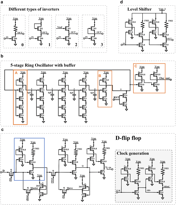
a Four different topologies for a low power inverter: a–0 standard inverter with resistive load. a–1 Diode connected n-FET. a–2 n-FET biased to control the current flowing. a–3 Cut-off n-FET configuration to utilize its leakage properties. b Schematic of the designed 5-stage ring oscillator, highlighting the 3 types of inverters used. c Schematic of the D flip-flop, highlighting the additional structure needed to meet power and timing criteria d Schematic of the Level shifter. Each circuit schematic includes the transistor’s W/L ratio, with all values expressed in micrometers.
Ring oscillator
The ring oscillator is the core module of the system. Ring oscillators use an odd number of inverters to generate a signal with a specific frequency. This odd number of inverters creates an astable circuit that continuously transitions between two states.
The frequency of one oscillation is roughly the inverse of the total time it takes for a signal to propagate through all the inverters. Therefore, the delay between the inverters is the primary way of controlling the oscillation frequency47.
In this design, the delay between the inverters mainly depends on two factors. First, the value of the capacitors connected between nodes, since higher capacitance values result in longer charging times and thus lower frequencies. There are two ways of increasing the capacitance. First, directly adding capacitors in between the inverters (and/or building the inverter gates with the highest parasitic48 capacitance possible by following the design manual from PragmatIC). Second, reducing the current that drives these capacitors, increasing the rise time and thus the time delay. To control the current supplied to such capacitors, we focused on the load component. Since p-FETs are not available in this technology, and large resistors require big areas and exhibit considerable variability, the simplest solution was to substitute the resistive load with an n-FET transistor48. Here, there are three topologies depending on how the n-FET transistor is biased:
-
1.
Diode connected n-FET (Fig. 2a-1): The gate is connected to the supply voltage. This solution provides too much current to meet the specifications.
-
2.
n-FET biased to supply a small current (Fig. 2a-2): This strategy is impractical since it needs additional circuitry to generate several bias voltages, consequently increasing the power budget.
In addition, process variations make the stable voltage references needed difficult to achieve.
-
3.
Cut-off n-FET49 (Fig. 2a-3): With this topology the only current going from source to drain is the leakage current, leading to two states:
-
a.
When transistor M0 is closed (conducting) the leakage current from transistor M1 is directed to ground, resulting in an output voltage near to 0 V.
-
b.
When transistor M0 is open (non-conducting) the leakage current from transistor M1 charges the parasitic capacitances on the output node, increasing the voltage.
Fig. 3: Performance characteristics of the wake-Up timer. 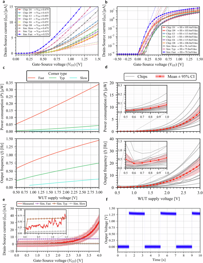
a, b Transistor characteristic curves in linear and logarithmic scales, respectively. Fitting dash-dot lines are used to calculate Vth and SS, respectively. Curves acquired with the transistor in linear region (Vds = 0.1 V) c Corner simulation results of the power consumption and frequency distribution against the supply voltage. d Power consumption and frequency distribution against the supply voltage for the 13 chips tested. e Leakage current vs Drain-Source voltage of an n-FET of 50 μm/0.8 μm size in cut-off configuration (VGS = 0 V). Data from simulations included for comparison. f Oscilloscope’s output while testing the wake-Up timer supplied with 0.7 V for the whole module and 1.5 V for the level shifter.
-
a.
This third topology (substituting the resistive load with an n-FET transistor biased in leakage mode (Fig. 2a-3)) is thus the solution that best minimizes power consumption. Nevertheless, the size of the transistors on the load and driving sides needs to be balanced. If the driving transistor leaks more current than its load counterpart, the load transistor will not be able to increase the output voltage from 0 V, because the driving transistor will drain the current to ground.
The ratio between the load and the driving transistors has been carefully matched in this design, so that the leakage current of both is minimized while the gate capacitance of the driving transistor is maximized, according to the technology’s documentation on parasitic capacitance. As a result, the output frequency decreased. Another way to reduce the frequency consists in adding more inverter stages. This has the detrimental effect of enlarging the total area: more inverters linearly increase the propagation delay, and this linear increase does not offer a substantial reduction in frequency compared to the cost in area. This is why we designed the ring oscillator with 5 inverters, as it is the minimum number of inverters required to ensure correct operation; simulations showed that using 3 inverters doesn’t work in this design.
While this ring oscillator shows picowatt levels of consumption and a reasonable area, it suffers from poor tolerance to process variations and temperature dependency. Unfortunately, in this technology the leakage current can exhibit significant variability. This implies that, despite the power consumption remaining low regardless of the process variations, the frequency of the ring oscillator can vary from chip to chip, as shown in the “Characterization” section.
Figure 2b presents the schematic of the ring oscillator in detail. The design uses three types of inverters: A and B (included in the loop), and C (that defines the output buffer). Inverters A were designed to minimize the leakage current and increase the gate capacitance as much as possible, maximizing the delay between these inverters. Inverter B was designed to deal with the extra capacitance added by the output buffer and its load transistor was optimized to handle higher leakage currents, resulting in less signal delay when compared to inverter A. However, as inverter B is directly driving the output buffer C, it plays a key role on the waveform shaping, and thus on maintaining signal integrity and an appropriate oscillation behavior. Finally, reset transistors can revert undesired stable states that may prevent the oscillation when powering on the device.
Frequency divider
The frequency divider is based on a basic asynchronous counter that eliminates superfluous transitions to reduce power50,51. The counter consists of a chain of D flip-flops, where only the clock input of the first flip-flop is connected to the WUT. The clock input of the following flip-flops is the negative output of the previous flip-flops (Fig. 2c). This design is based on the propagation of the least significant bit (i.e. each flip-flop represents a bit), where only the flip-flops that will change in the following count are effectively toggled with the clock arrival. The main advantage is that the asynchronous counter limits the dynamic power consumption to the flip-flops that toggle in each cycle. The main drawback is that every bit will toggle after the propagation delay of the previous flip-flop, and this delay can be troublesome in counters with a large number of bits. But this is not a problem in this design, because the counter works at low frequencies and can support delays of some nanoseconds (and even microseconds).
Figure 2c depicts the schematic of the frequency divider. In a chain of flip-flops, the frequency is proportional to the number of stages as:
where ({T}_{{in}}) and ({T}_{{out}}) are the input and output periods of the frequency divider, and ({n}_{{FF}}) is the number of flip-flops. Therefore, a chain of four flip-flops, Fig. 1b, divides the frequency by a factor of sixteen.
PragmatIC provides a non-validated D-flip-flop in its technology’s library. It is a common master-slave D-flip-flop designed with an R-NMOS topology. A counter, using four flip-flops from PragmatIC, supplied at 0.7 V with an input clock frequency of 1 Hz has a power consumption of ~2.46 μW in simulations, which is unacceptable for this design.
Nevertheless, taking advantage that the D-flip-flop from the technology library worked properly in simulations, the solution chosen in this design is the same as in the ring oscillator design: the circuit is slightly modified by initially replacing each resistor with a cut-off n-FET transistor.
Although the power consumption is effectively reduced, correct dimensioning of the flip-flop components is essential to trade off power reduction with reliable performance. For example, to meet the criteria in simulations, we needed to increase the leakage current by placing several transistors in parallel. This helps to increase reliability up to a certain point. Beyond this limit, further increases in current are minimal and insufficient in the worst cases. To solve this problem, a structure consisting of three transistors and one resistor was used instead of the n-FET transistor. Figure 2c shows such structure, highlighted in blue, together with the detailed transistor-level schematic of the frequency divider. This circuit was functional under all simulated cases and met the low power and high reliability criteria.
The frequency divider can work with clock frequencies of up to 7 kHz, which is adequate, considering that the ring oscillator generates a signal in the Hz range. Remarkably, the power consumption was only 6.8 nW, with each flip-flop consuming 1.7 nW, a hundredfold improvement compared to the frequency divider simulated initially. Such power consumption is obtained by supplying the counter at 0.7 V with an input clock signal of 1 Hz.
Level shifter
To operate the circuit at low power, voltages were maintained as low as possible. However, because the wake-up signal must drive external systems that operate at standard voltages, a buffer working as a level-shifter was included.
Figure 2d. shows the level shifter schematic. It uses a topology similar to that used in the frequency divider’s D-flip-flops and includes a load-side transistor paired with an R-NMOS inverter. This design choice enables the output to deliver a higher current, facilitating faster rising edge times. The level shifter can convert digital signals from 0.5 V to 6 V bidirectionally, with simulated rise and fall times of 66 µs and 77 µs, respectively, in signals of 1.2 V. To function properly, the level shifter must drive external devices with high input impedances ( > 100 MΩ). The simulated power consumption of the level shifter when shifting 1 Hz signals from 0.7 V to 1.2 V is 879 pW.
Characterization
Regarding fabricated circuits, we tested and validated 13 chips under different temperature and illumination conditions. In the following sections we present the results from the experimental test and compare them with the expected outcomes from the simulations.
Cut-off n-FET transistor
Simulations during the design of the circuit showed that using an n-FET transistor in a cut-off configuration, instead of using a diode connected n-FET or an n-FET biased with a positive gate voltage, minimizes power consumption as the transistor remains in the off state. Nevertheless, we validated the simulated results with the fabricated transistors, considering, as well, the potential impact of threshold voltage (Vth) and subthreshold slope (SS) on leakage currents.
Figure 3a, b present the transistor characteristic curves in linear and logarithmic scales, respectively. Figures also include the regression line (i.e. thin dash-dot line) used to calculate Vth and SS. The current was measured supplying 0.1 V at the drain terminal of the transistor to ensure that the n-FET is in the linear region. The results, obtained from 5 different transistors, show that the Vth ranges from 0.38 V to 0.45 V, and the SS ranges from 103.6 mV/dec to 115.8 mV/dec. These values validate that the transistor behaves consistently in the sub-threshold region under normal operating conditions, minimizing leakage currents when operated below the threshold voltage. The relatively narrow Vth range ensures that the transistors will have predictable switching characteristics, and the SS values indicate a relatively sharp transition between the off (cut-off) state and the on state, which also contributes to the low power.
Frequency and power consumption dispersion
Time counting at a limited power budget is the main goal of the WUT. For this reason, the key benchmark to characterize was the frequency generated and its associated power consumption. During the design of the WUT, the dimensions of the transistors were decided through simulations, looking for a tradeoff between power and robustness against process variability. Therefore, corner simulations using fast, typical and slow models were carried out. Figure 3c shows the post-layout simulations of the power consumption and the frequency of the WUT at different supply voltages, and at different corner cases. These results show that frequency and power consumption depend almost linearly on the supply voltage. This means that the major contribution to the power consumption is the static power, since the dynamic power consumption depends quadratically on the supply voltage. In fact, results from simulations demonstrate that the contribution of the dynamic power consumption of the WUT to the total power consumption is below 6%.
According to the simulation, the circuit can operate across a wide range of supply voltages, from 0.5 V up to 3 V; except in the slow corner case, where the circuit stops working below 0.9 V. The worst frequency and power consumption values appear in the fast corner, achieving a frequency of 1.45 Hz and a consumption of 330 nW when supplied at 3.0 V. Nevertheless, these values are still acceptable for our application. The WUT exhibits significant variability, with a tenfold difference between the slow and the fast corner cases. This variation is directly related to the use of the transistor’s leakage current to enable the ultra-low power capabilities of the ring oscillator and is further studied in the section of the “Ring oscillator”.
We assessed these predictions sweeping the supply voltage applied to the 13 chips tested from 0.5 V to 3.0 V. Figure 3d shows the frequency and power consumption measurements obtained in these tests in gray lines, with the mean values highlighted in red, and the 95% confidence interval represented by the shaded area. A comprehensive statistical analysis of the frequency and power measurements across the 13 tested chips is provided in Supplementary Table 1. This analysis includes mean values, standard deviations, variances, and coefficients of variation (CV), where CV represents the ratio of the standard deviation to the mean, offering detailed insights into the variability and performance consistency of our WUT design. The minimum supply voltage required to assure the correct function of the circuit in all the chips was 0.7 V, although results showed that most of the chips could work properly when supplied at 0.6 V. The frequency and power mean values, at 0.7 V, are 0.24 Hz and 26.8 nW, respectively, with CVs of 0.61 and 0.53. Before calculating the CV, Shapiro-Wilk tests were performed to confirm that the measured data follows a normal distribution. For frequency measurements, the CV ranges from 0.56 to 0.67, The CV for power measurements show similar values, ranging from 0.53 to 0.68. Therefore, we observe approximately 60% variability across all studied parameters.
At 0.7 V, experiments and simulations matched closely, showing frequency and power spreads across the devices between 0.1 Hz and 0.8 Hz, and between 20 nW and 170 nW, respectively. Contrary to simulations, there was no linear relationship between the supply voltage with frequency and power consumption, and both increased at higher rates for higher voltages. Given that the major contribution to the power consumption is static power, it is reasonable to assume that the leakage current might not be well modeled in n-FET transistors connected as reverse-biased diodes, leading to this discrepancy. Data in Fig. 3e shows that the leakage current in the test transistor follows a trend similar to that of the power consumption in Fig. 3d, supporting this idea. Figure 3e also includes the simulated leakage current for each corner, showing that the leakage current is modeled linearly and remains almost constant, which does not align with the more variable and increasing leakage currents observed in the measurements. This further confirms that the leakage current is not properly modeled in the n-FET transistor.
Additionally, it is also evident that both frequency and power consumption distributions from experiments in Fig. 3d spread similarly to the corner-case simulations, with near to a tenfold difference between the worst and best performing dies. Such distribution is due to the process variation on the leakage current, mainly generated by the n-FET transistors on the load-side of each gate. Since these transistors are placed near each other in the layout, their properties should be mostly affected by chip-to-chip variations rather than by process mismatches. Therefore, the close-by transistors exhibit similar properties that add up, leading to extreme cases where they collectively cause the signal to be significantly faster or slower. No alternative to narrow down this variability has been found, without compromising other vital features such as area, power consumption or absolute frequency.
Finally, Fig. 3f shows the WUT’s output signal when supplying 0.7 V to the ring oscillator and the frequency divider, and 1.5 V to the level shifter. The result is a clean and stable signal of 50% duty cycle, with similar rise and fall edges, found consistently in all the tested dies. Signal amplitude decreased slightly (down to 1.3 V), possibly because of the small parasitic resistive loads intrinsic to the measurement setup, that deviate from the ideal capacitive loads assumed by design.
Effects of temperature
At this stage, the transistor models provided by PragmatIC do not fully reflect their temperature-dependent behavior. Consequently, it was not possible to predict (and thus compensate by design) the influence of the temperature on the WUT operation. Therefore, we analyzed this aspect afterwards, in temperature-dependent experiments with the actual devices.
Initially, the effect of temperature at transistor level is studied. For this test, the transistor is biased in linear region and then the temperature is controlled, starting from 25 °C, room temperature (RT), to 85 °C in 10 °C steps. After that, the transistor is cooled down to RT. Literature reports that when temperature increases, Vth of IGZO TFTs typically decreases, which can lead to higher leakage currents and affect the overall power consumption of the circuit52. The SS also tends to worsen with increasing temperature, leading to less effective transistor switching and higher subthreshold leakage currents53. Figure 4a, b present the transistor characteristic curves at different temperatures in linear and logarithmic scales, respectively. They also include the regression line used to calculate Vth and SS. Both figures show that when temperature increases, the Vth decreases and the SS value increases, which is in line with the reported in the literature. In addition, after cooling back to RT the transistor and allowing a 20 min stabilization period, results show that the Vth and SS return to their initial values.
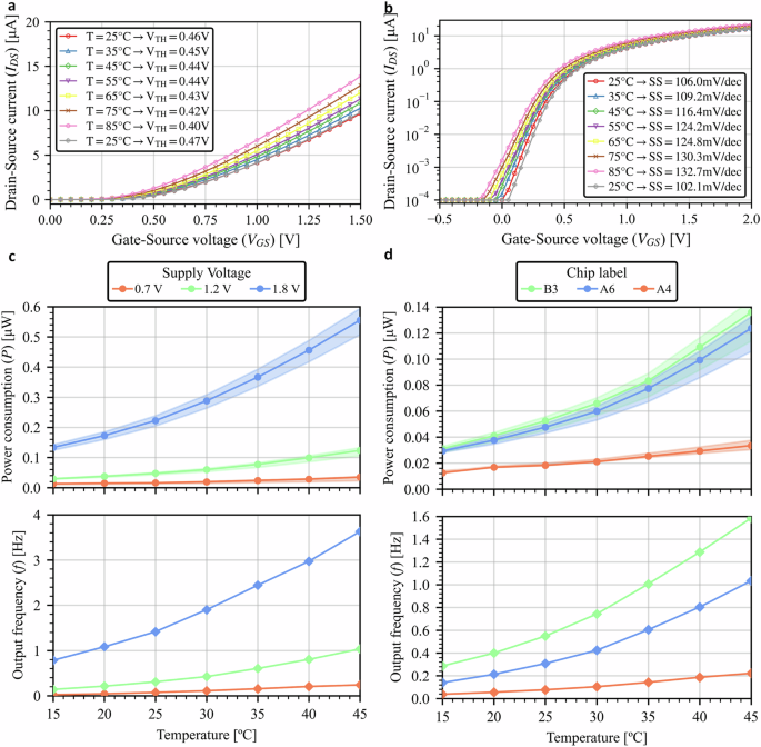
a, b Transistor characteristic curves at different temperatures in linear and logarithmic scales, respectively. Curves acquired with the transistor in linear region (Vds = 0.1 V) c Ring Oscillator’s response to temperature variations 15 °C–45 °C. d Frequency and power response of three dies (B3, A6, A4) to temperature variations. The chips were supplied at 1.2 V.
After that, the effect of the temperature on the WUT is studied. Figure 4c depicts the impact of temperature on the power consumption and output frequency of the WUT. In this test, three different supply voltages were used (0.7 V, 1.2 V and 1.8 V), in order to observe also the combined effect with the supply voltage. As expected from the transistor level results, increasing temperature significantly modifies the frequency and power consumption of the circuit, showing a fourfold increase as the circuit warms from 15 °C to 45 °C, being the worst case at the highest supply voltage and highest temperature. Additional tests to illustrate the temperature effects in different chips (3 devices at 1.2 V, Fig. 4d) showed that, despite initially having different frequency and power consumption values, their rate of change due to the temperature variations seems similar among chips. Anyhow, the WUT worked properly across the tested temperature range with an acceptable variability for the purpose of its application, as discussed below.
Effects of light
IGZO is an oxide natively sensitive to light. When illuminated, the material generates additional charge carriers, changing the behavior of the devices (e.g. variation in the transistor’s threshold voltage54) and reducing its stability and reliability (e.g. light may accelerate the degradation of the material55). Studies on the light effect on the WUT are further relevant since the chips are supplied without packaging.
Tests started in a dark environment (i.e. 0 lux set right after connecting the die with probes) maintained until the output frequency stabilized. Then, a light source (i.e. 30k lux from the LED lamp of a microscope) was turned on to observe its influence on the electrical signals. Figure 5a illustrates the result of this test in two different chips. It took more than one hour for the output frequency to stabilize to the double of its initial value. As an immediate response to the 30k lux of light, frequency drifted up again, first suddenly and later at a reduced pace. Figure 5b shows the output frequency response of the WUT to an on/off light test. The light was off for the first 30 min, then turned on for the next 30 min, and finally turned off again for the last 30 min. After each 30-minute phase, the frequency of the WUT did not stabilize, but it can be observed that by the end of the test, the WUT did not return to its initial frequency values. Similar qualitative trends were observed in the devices studied.
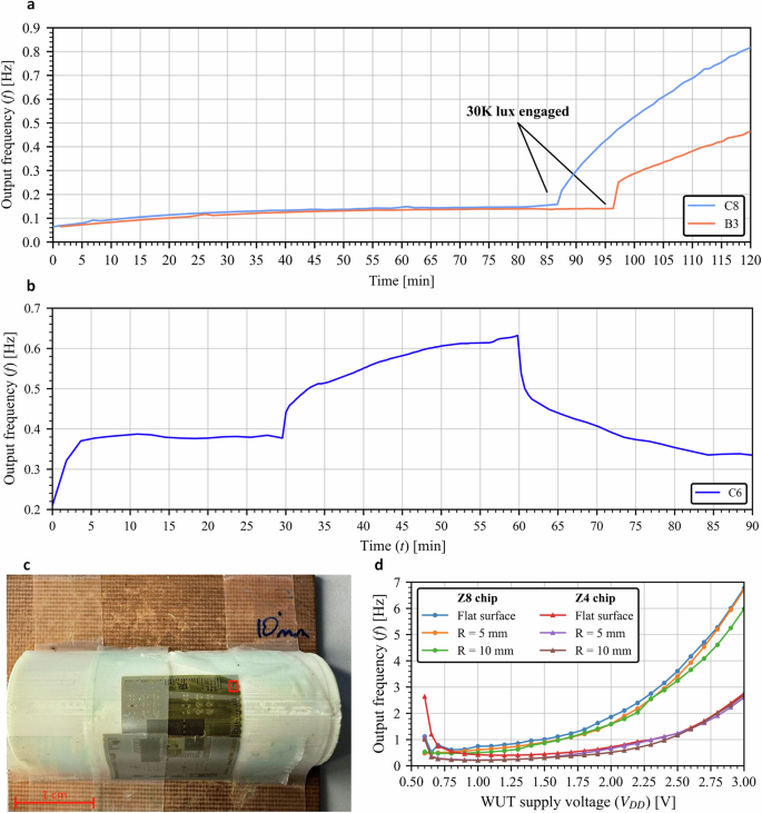
a Drift and light sensitivity effects when the Wake-Up timer is powered up. The Wake-Up timer stabilizes completely after the hour mark. At roughly the 90-minute mark, a LED lamp engages 30k lux directly onto the chip and instantly a frequency drift is noticeable. Different chips present slightly different frequency variation patterns. b Output frequency response of the WUT to an on/off light test. Light is on from 30 min to 60 min. c Test platform for tensile stress testing. The chip is placed on a 3D-printed convex piece d Output frequency response of the WUT, for two different chips (Z4 and Z8), under tensile stress testing. The chip is placed on three different surfaces: a flat surface and two convex surfaces with bending radius of 5 mm and 10 mm, respectively.
Effects of bending
The use of flexible substrates permits to apply to the designed circuits various mechanical stresses, which affects their performance. Circuits located in the upper side of the substrate were submitted to tensile stress due to the bending of the substrate in convex configuration. These tests were done by placing the WUT on different surfaces.
First, the WUT was placed on a flat surface, and then on convex surfaces with bending radius of 5 mm and 10 mm, respectively. Figure 5c shows the test setup using the convex surface with the long side of the WUT, measuring 432 microns, aligned with the direction of maximum curvature on the convex surface. With this arrangement, the WUT bends with a length-to-bending radius ratio of approximately 1/10 and 1/20, respectively.
Figure 5d shows the frequency measured with the circuit on the different surfaces for two different chips labeled as Z4 and Z8. These chips were fresh-new and untested and were selected to evaluate the performance consistency of our WUT design under bending conditions. Results show minimum frequency variations when the chips are curved. Frequency variations between chips, specially from 1.25 V to 3 V, are consistent with the results presented in Fig. 3d.
Discussion
To the best of our knowledge, this is the first report of a WUT specifically designed for FlexIC technologies. The circuit generates mean wake-up frequency of 0.24 ± 0.15 Hz, which is an ideal value to monitor periodically human-centered activities. At the same time, mean power consumption is as low as 26.7 ± 14.1 nW. These are excellent figures, considering the constraints imposed by the n-FET FlexIC technology. When compared to other similar technologies (see Fig. 1a), our WUT design achieves nearly two orders of magnitude improvement in power consumption, setting a new benchmark for power efficiency in FlexIC technologies. Although our design still consumes more power than state-of-the-art WURs and WUTs implemented in Si CMOS, the results represent a significant step toward closing the performance gap between flexible and traditional silicon-based electronics.
Out of the many different Wake-Up topologies proposed before56,57, the simplicity of the ring oscillator and the frequency divider accommodates well the limited range of devices available in the resistive-load technology. Both circuits are digital devices that, if designed with the process variations in mind, offer a robust way to indefinitely divide the resulting frequency with low power needs. Given that the ring oscillator’s area is approximately 1.5 times larger than that of a flip-flop, using a frequency divider in this design is the best option to divide the oscillator’s frequency by a factor higher than 2 without significantly increasing area usage.
Our design also shows that it is possible tackling low power applications with FlexIC in general (and with the PragmatIC’s 0.6-µm n-type technology in particular). This goes beyond the range of typical applications recommended by the manufacturer, that are illustrated in many literature examples way more complex and power hungry, like time-domain multiply-accumulate engines58 or micro-processors35.
In a gate-level comparison, other FlexIC designs report gate power budgets in the nanowatt regime34, while our gates consume picowatts. However, the rapid increase of the leakage current with the operating voltage in the PragmatIC technology calls for a word of caution when generalizing this comparison.
The CV values for frequency and power measurements indicate substantial variability in the functional behaviors. Still, this is consistent with the variability levels predicted by the simulation models provided by Pragmatic. The frequency values (at low voltages) fall within the wide range defined by fast and slow corner cases in the simulations. In contrast, power measurements vary similarly but deviate quantitatively from the predicted ranges, possibly due to known differences in the model description of the leakage current. Regarding the multiple effects that influence the value and stability of the output frequency, none of them makes it critically unreliable nor hampers its practical use. The dependence with the supply voltage can be prevented with a well stabilized voltage source. The chip-to-chip differences due to processing can be corrected after individual calibration, either adjusting the supply voltage or setting chip-specific counter limits in a dedicated register. The effects of the temperature can be similarly reverted, provided that the external circuit can access temperature information and set the appropriate temperature compensation value before entering in sleep mode. Note that the working frequencies are so slow that no self-heating is expected. So, ambient changes will be the main source of temperature variation. In addition, bending effects do not introduce significant changes in the performance of the circuit, ensuring stability even under mechanical stress. Regarding light, the most effective approach would be directly blocking it, either including top metal layers in the layout (as recommended by PragmatIC) or just using a non-transparent encapsulation.
All in all, this work demonstrates the versatility of the current FlexIC technologies and highlights the high efficiency of our proposal for energy-critical applications.
Methods
Design considerations
We began the design of the WUT with the 1.2 version of Process Design Kit (PDK) from PragmatIC, where the minimum channel length was 0.8 µm. But before layout completion, the PDK was updated to version 2.1 and the minimum channel length was reduced to 0.6 µm. In consequence, some modifications to our design were needed to adapt the schematic (i.e. modifying the values of some parasitic devices) to the new PDK and to accommodate the layout to the new manufacturing process. The new layout reduced the total size by 2/3ds.
Regarding the change in the minimum channel length, in the schematic transistors with a channel length of 0.8 µm can be grouped into four categories: transistors on the load side (i.e. drain connected to the power supply), transistors in series with a resistor, driving transistors (i.e. source connected to ground), and pass-gate transistors in the flip-flop.
In the first case, reducing the channel length slightly increases power consumption. In addition, most of these transistors have a width much larger than their channel length, therefore changing it does not result in significant improvements. In the second case, reducing channel length also increases power consumption because it lowers the total resistance of the resistor-transistor combination. In the third case, reducing the channel length decreases power consumption, but it also increases the signal’s fall time. For example, simulations of the level shifter show that reducing the channel length of transistors near ground decreases power consumption by 0.2 µW but increases the signal’s fall time by 1 µs, which breaks the balance between rise and fall times. In the last case, reducing channel length decreases parasitic resistance by 25% in simulations, but this does not significantly improve the WUT’s performance.
Reducing the channel length of transistors did not bring significant improvements in WUT power consumption and even worsened fall time. Therefore, the channel length in the design remained at 0.8 µm.
Characterization
Cut-off n-FET transistor
The transistor characterization tests required contacting its terminals with three probes in a probe station. A VDS voltage of 0.1 V was applied, and the gate terminal was swept from −1 V to 2 V using an Agilent 4155 C SPA source, which also measured the IDS current.
Frequency and power consumption distribution
In the current PDK (i.e. 2.1) version, Monte Carlo simulations are not available, and many temperature effects are not modeled. Therefore, characterization was focused on comparing the corner models to the tested properties of the WUT. A Python script, running on a computer, controls and acquires data from the B2912A precision source/measure unit and the MSOX6004A oscilloscope. Each test consists in placing the chips in a probe station with vibration isolation, engaging the probes, biasing the chip, connecting its output to the oscilloscope, and finally waiting 10 min for the chip to adjust to the light/source conditions. After that, the python script drives the B2912A source, sweeping the supply voltage and measuring the supplied current to calculate the power consumption. In parallel, the Python script also controls the MSOX6004A oscilloscope to measure the oscillation frequency and power consumption values. In particular, the Python script changes the supply voltage of the circuit, waits 30 s to take 10 measurements of the frequency with the MSOX6004A while acquiring 500 samples of the current consumption with the B2912A. Once the voltage sweep is finished, the chip is removed, and the next one is engaged. A total of 13 chips have been characterized with this procedure. All chips were glue-taped onto a copper PCB substrate and fixed to the probe station with a vacuum pump. This test was done at room temperature (20 °C). In addition, as the WUT was designed to drive a capacitive load, the output connection between the circuit and the oscilloscope was not direct. An amplifier, with high input resistance (OPA2182 from Texas Instruments) and configured as a voltage follower, was placed in between to assure that the oscilloscope’s input impedance did not affect the measurements.
Effects of temperature
For the chip characterization, the use of a bulky probe station setup prevents us from placing it in a climate chamber. Instead, we used a thermal chuck, that can only provide a limited range of temperature. Still, two types of tests were conducted to analyze the effects of temperature on the circuits: one for the WUT and another for the characterization of the n-FET transistor. Since the number of pads, distance between bond pads and probes required for each test are different (i.e., 5 probes for the WUT and 3 probes for the transistor), two different thermal chucks were used for practical reasons, basically to assure that we could contact the bond pads in each case without damaging the chip.
In the transistor tests, the I-V temperature measurements were obtained using an Agilent 4155 C SPA + Cascade Microtech M150 with AC3 thermal chuck. The measurements were performed from RT (i.e. 25 °C) to 85 °C with a step size of 10 °C and a final curve was extracted after the device cooled down to RT.
Before the measurements, some transfer plots were extracted to stabilize the device (usually 1 or 2 are needed until device stops the early shifting of Von). Also, before each measurement, when the desired temperature was reached, a 20 min stabilization was made to ensure that we have a uniform temperature across the whole substrate.
In the WUT tests, temperature was controlled using the PCT1 temperature-controlled breadboard based on thermoelectric elements from Thorlabs©. The device can maintain any temperature between 15 °C and 45 °C. We analyzed the temperature variation for different dies at three different supply voltages: 0.7 V, 1.2 V and 1.8 V. The test started selecting a supply voltage and introducing a value of 15 °C to the Thorlabs© PTC1 temperature-controlled breadboard; when the circuit reached the desired temperature, the frequency and the power consumption were acquired with the same procedure as in the previous section. The temperature was then raised in increments of 5 °C, introducing the next temperature value manually in the software application provided by Thorlabs©. The test stopped when the temperature reached 45 °C. Then, the temperature-controlled breadboard returned to 15 °C and switched to the following supply voltage.
Effects of light
During the initial characterization of the chip, it was noticed a drift effect on the WUT’s frequency. Further investigation allowed us to conclude that the drift effect was noticed when starting up the circuit, with the output frequency increasing for some minutes. As confirmed with the foundry, there is an impact of light on each component performance, that is different depending on the device considered. For example, resistors show a noticeable influence on light, with relaxation times higher than 12 h, while transistors only show backlight influence, with relaxation times around 10 min. The current design is not covered with metal layers, which are now recommended to prevent light impact on the performance of the chip.
After verifying the impact of the light on the performance of the circuits, all the chips were measured following the same procedure. First, the probes were engaged to the bond pads with the microscope’s spotlight glazing over 30k lux onto the WUT. Second, an initial verification that the circuit was working properly was made, with the light on, to assure that the probes were properly engaged. If the circuit worked properly, the spotlight was turned off and the voltage source was switched off. Third, after waiting for 10 min, the WUT was supplied, and the test started.
30k lux is considered strong sunlight (“bright sunlight” typical of the early morning or late afternoon, or a slightly cloudy day), but it is not the full intensity of direct sunlight. Such value was selected as a reasonable worst-case, for illustration purposes.
The effects of light suggest that the circuit must be protected from direct light for a predictable and stable operation, e.g. either by covering it or by means of packaging. This would minimize the influence of light from reflections, backlight illumination, or other indirect sources. Since preventing light is the most reasonable course of action, we considered it did not require a further, more thorough analysis.
Effects of bending
Static performance characterization of the WUT under different tensile stresses was performed by placing the circuit on convex surfaces with a curvature radius of 5 mm and 10 mm. Given the rectangular layout of the WUT, the long side of the WUT was aligned with the direction of maximum curvature on the convex surface to maximize the tensile stress, achieving a length-to-bending radius ratio of approximately 1/10 and 1/20, respectively.
Both convex surfaces were 3D printed using the Ultimaker s5 printer, which has a Z-axis precision of 0.1 mm. This means that the top of the convex surface is not perfectly round. To avoid unwanted effects during the test, the WUT was placed along the curvature rather than at the top. The chip was fixed to the convex surface with tape.
The tests were performed using the same set-up as in frequency and power consumption tests. Although the probe station was placed in an anti-vibration table, positioning the probes was extremely challenging, resulting in the destruction of some bond pads after the tests. Given the layout of the WUT, the pads distribution and the need to test it with the probe station, it is impossible to perform other mechanical characterizations like compressive stresses or dynamic bending tests.

Responses