Antiferromagnetic domain wall memory with neuromorphic functionality

Introduction
Neuromorphic computing concepts are becoming increasingly important to address the ever-growing need for energy-efficient processing of massive amounts of information. Inspired by the function of the biological brain, various concepts of neuromorphic computing have been developed based on artificial neural networks, where threshold-activated, firing neurons are interconnected with a multitude of synapses, and where learning of the network is performed by varying their analog synaptic “weights”1. Today, software implementations of neural networks are widely used for facial or pattern recognition, language translation, search engines and in GPT-like large language models. Unfortunately, as the complexity of their tasks increases, they consume more and more energy, making them eventually unsustainable. Therefore, for the full realization of the potential of artificial neural networks, advancement in the hardware level, such as using resistive phase transitions or nonlinear magnetization dynamics to mimic the functionalities of synapses and neurons, are being extensively explored2,3,4,5,6,7,8. The majority of recently proposed memristor-based neuromorphic devices are based on profound changes of the internal configuration of the device such as via ionic motion or changes in crystal structure because of thermal effects, which are not highly reliable9,10,11,12.
One approach to realize energy-efficient artificial synapses are magnetic systems where the usually non-volatile synaptic weight is encoded in the number of magnetic nanostructures such as skyrmions13,14 or in the position of magnetic domain walls15,16,17,18. A prominent example of a non-volatile magnetic synapse is a magnetic tunnel junction heterostructure, where partial magnetization reversal is triggered by current-induced domain wall motion via spin transfer torque17. However, a major drawback of artificial synapses based on ferromagnetic systems is the magnetic stray field that is generated globally by the entire magnetic configuration and can affect the magnetic nanostructures, especially during the writing process. This long-range interaction, combined with thermal excitations and probabilistic fluctuations of the magnetic moments, can cause stochastic behavior of domain wall pinning and depinning and prevent well-controlled and reproducible writing of analog synaptic weights.
Alternative approaches therefore consider the implementation of systems featuring arrangements with compensated magnetic moments, such as in antiferromagnets19,20,21,22 or in altermagnets23,24,25. These zero net-moment systems offer non-volatile memory functionality without unwanted crosstalk caused by magnetic stray fields. In addition, they are inherently more robust against modest external magnetic fields and, most importantly, their exchange-field enhanced spin dynamics can enable very fast picosecond writing26,27, which is another important property that permits a reduction in power consumption. Furthermore, extremely fast domain wall motion driven by current-induced spin-orbit torque has been observed in synthetic antiferromagnet and ferrimagnet systems28,29,30.
Recent progress towards the development of antiferromagnetic synaptic devices has been realized, for example, in exchange-coupled ferromagnetic-antiferromagnetic hybrid systems. In this approach, the synaptic weight written by the current-induced spin-orbit torque (SOT) is read by the anomalous Hall effect and corresponds to the ratio of up and down-oriented ferromagnetic domains. The key here is that the ferromagnetic domain structure is stabilized by exchange coupling to the antiferromagnetic layer31,32.
Alternative concepts use only the antiferromagnet as a functional part. Here, electrical or optical excitations heat the antiferromagnetic film close to its Néel temperature, causing the initially large antiferromagnetic domains to fracture into multiple submicron domains, thereby bringing the antiferromagnet into a high-resistance multidomain state. The subsequent temperature-dependent recovery back to a low-resistance, the large-few-domain state can be exploited in neuronal networks based on spike-timing-dependent plasticity, but realizing non-volatile functionality is impossible with this approach33,34. Volatile states have also been observed after 90∘ orthogonal Néel-order SOT switching in CuMnAs crossbar devices21,22. They typically exhibit a characteristic stretched exponential decay. This unstable property is in striking contrast to the non-volatile SOT-driven 180∘ Néel vector reversal that we have previously observed in CuMnAs35,36 and that we will now exploit in a synthetic antiferromagnetic system with nominally compensated magnetic moments.
In this work, we use a compensated synthetic antiferromagnetic (SAF)37 system with perpendicular magnetic anisotropy, where the non-volatile analog information is stored in stable reversed antiferromagnetic domains with Néel vectors pointing up and down along the magnetic easy axis. The combined parity and time reversal (({{{mathcal{PT}}}})) symmetry of the SAF multilayer allows us to exploit the spin-orbit torque-driven 180∘ domain wall motion to modify the ratio between reversed antiferromagnetic domains and to access the analog information by nonlinear transport measurements. We identified a very high level of reproducible writing, which we attribute to the absence of magnetic stray fields in the compensated antiferromagnetic system.
Results
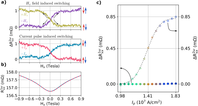
In Fig. 1 we present the most important features of our antiferromagnetic domain wall memory. As illustrated in Fig. 1a, it consists of two ferromagnetic layers antiferromagnetically coupled by the Ruderman-Kittel-Kasuya-Yosida (RKKY) interaction through a thin Iridium layer. Both ferromagnetic layers are comprised of Cobalt-Nickel multilayers and exhibit perpendicular magnetic anisotropy. The entire stack is sandwiched between two nonmagnetic Platinum layers, in which, via the spin Hall effect current-induced spin accumulations are generated with opposite polarity at the interfaces to the magnetic layers38,39.

a Stack structure of the perpendicularly magnetized SAF. Note that due to SHE, at the interfaces Pt / FM, it is generated spin accumulations (σi) with opposite directions, resembling the Néel spin-orbit torque. b Anomalous Hall effect measurement showing four distinct magnetic states. c The change in 2nd harmonic longitudinal resistance as a function of the pulse amplitude at Hx = 0.9 T. The dark dashed line is the result of fitting the data to a cumulative function of a Gaussian distribution, or error function. As inset, the pulse sequence used to probe the dependence of the switching signal on the pulse height. Firstly, a strong negative pulse is applied to reset (Res) the device to the AFM state 0. The write operation (W) is performed by a positive current pulse and lastly, AFM state is read (R). This sequence is carried out 10 times for each current density. The reading of the state is done over a range of 1 minute, and the mean value of this time is calculated. Each point represents the average of the calculated mean value of the 10 individual readings. The error bars are the standard deviations around the corresponding mean values. d, Bubble-like domain distribution observed with magnetic force microscopy (MFM) after the sample was set into a multidomain state with a writing current pulse.
The magnetic properties of the SAF system become apparent when an external magnetic field is applied along the magnetic easy axis perpendicular to the sample plane. The anomalous Hall effect (AHE) signal is measured of a Hall-bar patterned structure as the field sweeps between ± 0.9 T (Fig. 1b). For large fields above 250 mT, corresponding to the easy-axis spin-flip field, the RKKY exchange interaction no longer sustains the antiferromagnetic order. The large AHE signals of ± 50 mΩ indicate then the ferromagnetic states when the magnetizations of the two layers are forced to align along the direction of the applied magnetic field. AHE and magnetometry measurements (see Supplementary Material section 1) also confirm that the system is in an antiferromagnetic state at applied fields below the spin-flip field. The small hysteresis in the AHE signal at low fields is a signature that the two exchange-coupled layers are not fully equivalent. We can make use of this experimental imperfection to set the stack into one of the two fully polarized antiferromagnetic states at zero field. This can be done by applying first a positive or negative magnetic field Hz larger than the spin-flip field. In the Supplementary Material section 4, we demonstrate that slightly unequal layers do not affect the functionality of the memory device. Additionally, a detailed analysis on how to infer the antiferromagnetic state after a Hz field was applied is shown in Supplementary Material section 7.
We detect the analog information in the antiferromagnetic memory by nonlinear transport measurements and therefore do not rely on the detection of uncompensated moments40,41. The underlying concept of nonlinear magnetotransport measurements is that the probe current flowing through a ({{{mathcal{PT}}}}) symmetric antiferromagnet perturbs the antiferromagnetic state depending on its polarization. The current-dependent perturbation in turn affects the probe current flowing through the antiferromagnet, i.e. there is a probe current-dependent change in resistance from which the antiferromagnetic order can be determined35,42,43. In our ({{{mathcal{PT}}}})-symmetric SAF structure, we can explain the nonlinear response by the presence of a Pt layer on top and bottom of the two magnetic layers within a toy model as shown in the supplementary Fig. S4. The model implies that an electric current induces non-equilibrium spin polarizations and the corresponding effective spin-orbit fields can deflect the antiferromagnetically coupled magnetizations of the two Co-Ni multilayers. Combined with anisotropic magnetoresistance, spin-Hall magnetoresistance and giant magnetoresistance as quantified in Supplementary Material section 3, the deflection leads to a second-order response (delta {R}_{xx}^{MR}({j}_{x})) of opposite sign for reversed Néel order. (delta {R}_{xx}^{MR}({j}_{x})) also changes sign with opposite current polarity. It therefore can be detected by a homodyne measurement of the 2nd harmonic signal. Note that (delta {R}_{xx}^{MR}({j}_{x})) also changes sign when the external magnetic field ({overrightarrow{H}}_{x}) is applied in the opposite direction. A more detailed discussion about the nonlinear magnetoresistance response can be found in the Supplementary Material section 4.
We apply an alternating probe current through the Hall bar device and focus on the nonlinear response of the longitudinal signal (({R}_{xx}^{2omega })). In Fig. 1c, it is shown a dependence of ({R}_{xx}^{2omega }) on the current density of the writing pulse. It does not show a step-like dependence expected from a complete reorientation of the magnetic order at a specific critical current. Instead, a smooth non-linear curve between the two fully saturated states is observed, with multiple levels in between. Such behavior results from the partial switching across the sample allowing both antiferromagnetic states to coexist with a given ratio. This adds extra functionality to the system as an analog memory, where the signal-to-noise ratio of the measurement limits the number of different states. In antiferromagnetic films, stray field effects are negligible, so that the domain structure is completely dominated by the magnetic anisotropy and consequently a single domain state is expected as the magnetic ground state. In real systems, however, current-induced domain nucleation starts at local defects, which in our case are mainly located at the device boundaries. Once inverted antiferromagnetic domains are formed by SOT pulse-driven domain nucleation and domain wall propagation, they remain stable even when the pulse is turned off. Size and position are thereby only determined by minimizing the length of the surrounding domain wall in combination with domain wall pinning.
The writing procedure was done while applying an external magnetic field along the Hall bar direction and with a magnitude of Hx = 0.9 T, close to the hard-axis spin-flip field of about 1.1 T. Before each electrical pulse one strong pulse with negative polarity was applied to reset into an antiferromagnetic single domain state (inset of Fig. 1c). At each current density, the measurement was repeated ten times and its mean value of the average over 1 minute is plotted. The error bars correspond to the standard deviation of the average value. Importantly, rewriting the memory by repeating exactly the same writing procedure 10 times shows only a small variation of the nonlinear response among individual measurements, which is well within the signal-to-noise ratio of each individual measurement.
The presence of a distribution of antiparallel (AP) domains of opposite polarization within the sample is confirmed with magnetic force microscopy (MFM). Large AFM domains spanning microns and surrounded by nm-sized domain walls are present compared to the small nanoscale domains often attached to inadvertent crystal defects as observed in a crystal AFM as CuMnAs44,45,46. Interestingly, a closer view to the domain walls shows that they have a brighter contrast, consisting of darker and lighter stripes that lie together along the domain wall47,48. The double stripe contrast stems from a net dipole moment generated by the slightly twisted antiferromagnetic domain wall, as a result of the dipole interaction between layers and / or the presence of Dzyaloshinskii-Moriya interaction (DMI) due to the Pt/Co-Ni interfaces at the top and bottom of the multilayer stack. The always dark/bright MFM contrast at the domain boundaries following the up/down polarization of the corresponding domains reflects the locally generated dipolar field. For example, in the bubble domain seen in Fig. 1d, the lighter (darker) stripe is always adjacent to the brighter (darker) domain. The same is observed throughout the whole sample. A more detailed analysis of the domain wall profile can be found in Supplementary Materials section 7.
To proof that the nonlinear response signal (({R}_{xx}^{2omega })) is related to the relative sizes of reversed antiferromagnetic domains, we compare the 2nd harmonic signal with the distribution of the AFM domains imaged with MFM. The measured nonlinear response signal which corresponds to the 2nd harmonic signal prepared in a desired multidomain state imaged in MFM is shown in Fig. 2a. For setting a reference range two oppositely saturated states were electrically written before a weaker in magnitude pulse generated a multidomain state. The corresponding nonlinear response yields an analog signal of 0.68 ± 0.05.
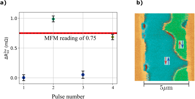
a Electrical preparation of the multidomain state prior to the MFM scan. The first three pulses with a large magnitude and alternating polarity are applied to drive the SAF system into fully polarized single-domain states of opposite Néel vector orientations. The corresponding nonlinear magnetoresistance values serve as reference values for the measurement performed after the last fourth pulse, which creates a multidomain state. From the electrical measurement a ratio of (68 ± 5)% population ratio between AFM domains with Néel vector up and Néel vector down is expected, while we find a (75 ± 1)% ratio when analyzing the MFM scan. The dark dashed line corresponds to the ratio between the integrated areas of the two oppositely oriented domains observed in MFM, and the red area its the error bar. b Section of the MFM scan highlighting large magnetic domains as blue and green regions (edited colors for clarity).
The nonlinear longitudinal signal originates from the area between the two longitudinal contacts (Supplementary Material section 2), which we scanned by MFM. Figure 2b shows a section within the main channel of the Hall device, where two distinct regions colored blue and green are observed, corresponding to domains with opposite Néel vector. Integrating the area of the both types of domains yields a ratio of 0.75 ± 0.01, which is in good agreement with the electrical measurement of ({R}_{xx}^{2omega }). The multidomain state sensed by nonlinear magnetoresistance measurements is proportional to the difference between the area of the reversed domains with the Néel vector “down”, Adown, and the total domain area Aup + Adown, hence (Aup − Adown)/(Aup + Adown) and the corresponding analog signal of the memory shown in Fig. 1c is therefore equivalent to Adown/(Aup + Adown).
The non-volatile character of the antiferromagnetic domain wall memory becomes apparent when considering that the MFM measurements were performed various days after the multidomain configuration was created and measured electrically. The non-volatility is ascribed to the energetically degenerate AFM states with reversed Néel vector separated by a high magnetic anisotropy barrier. The electrical writing requires an in-plane magnetic field, in order for the switching to be deterministic. Also, the in-plane magnetic field lowers the energy barrier separating the two AP states, decreasing the required onset current for efficient switching (see Supplementary Material section 6).
The non-volatile functionality is also confirmed by measurements shown in Fig. 3, where a multidomain state was prepared by an electrical pulse and detected by measuring the ({R}_{xx}^{2omega }) signal. We first set the reference range corresponding to both fully polarized reversed antiferromagnetic states, using a sequence of 3 saturating current pulses ( − Ip, Ip, − Ip) with Ip = 1.83 × 10⁷ A/cm2 at Hx = 0.9 T. Subsequently, a positive pulse of weaker magnitude of 1.6 × 10⁷ A/cm2 is applied, in order to generate a multidomain state. The nonlinear resistance signal ({R}_{xx}^{2omega }) is measured and then the magnetic field is switched off. After 60 minutes, we switch on again the magnetic field, remeasured the multidomain state and finally apply two saturating current pulses to generate two oppositely saturated reference states. Comparing the values measured directly after preparing the multidomain state and remeasured 60 minutes later, we observe only a small deviation within the error bars of the measurements. This confirms the stability of the multidomain state even when an in-plane magnetic field of Hx = 0.9 T has been switched off.
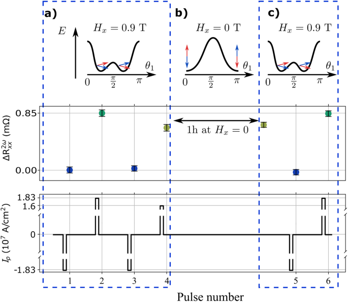
After the preparation of a multidomain state at Hx = 0.9 T (a), the external field is switched off for 1 h (b). The multidomain state is probed again after the magnetic field is turned on again. The measured signal equals the first value measured immediately after the multidomain state preparation within error bars and with respect to the two oppositely saturated states (c). On top, an illustration of the energy landscape as a function of the polar angle of both magnetic moments, for different magnitudes of the external field. It is assumed a cut of the energy landscape at θ2 = π − θ1, where θi stands for the polar angle of the magnetization in the layer i Each point in the ({R}_{xx}^{2omega }) signal is the average over 1minute reading and the error bar the standard deviation. Below, it is shown the sequence of pulses used throughout this measurement.
Discussion
In this work we have realized a non-volatile analog memory working at room temperature and based on a magnetically compensated synthetic antiferromagnetic heterostructure in which the information is encoded in the ratio between reversed antiferromagnetic domains. The memory is reproducibly written by current-driven antiferromagnetic domain wall motion and read by nonlinear magnetotransport measurements.
Synapses in the brain modify their synaptic weight as a function of the number of pulses per unit time which is known as spike-timing-dependent plasticity (STDP). Our antiferromagnetic analog memory does not show STDP, but rather pulse-“amplitude”-dependent plasticity with a persistent strengthening or weakening of the synaptic weight depending on the amplitude of the current pulses. Modification of the analog information is possible if either the magnitude of the current pulse amplitude is greater than the magnitudes of all previous pulse amplitudes, or if the polarity of the current pulse has been reversed with respect to the last pulse. In Supplementary Material Section 5, we show the experimental verification of this writing characteristic. We attribute the generation of the multidomain state to current-induced domain nucleation at defects followed by current-driven antiferromagnetic domain wall motion and argue that both processes are driven by damping-like spin-orbit torques. A comparison of the writing behavior with an applied in-plane magnetic field along and perpendicular to the writing current-pulse direction confirms our interpretation (see Supplementary Fig. S6). Most importantly, we can exclude that thermal effects randomly generate multidomain states. Moreover, since the writing process involves initiating domain wall nucleation and propagation, the magnitude of the write pulse must always be above a threshold current. This threshold current can be controlled by the strength of the applied in-plane magnetic field Hx, as shown in the Supplementary Material section 6 in Fig. S7.
To demonstrate that the absence of a stray magnetic field is the key to the remarkable reproducibility in writing the analog information, micromagnetic simulations are performed by using the open-source GPU-accelerated mumax3 solver49,50. For comparison, we investigated current-induced domain wall propagation in the SAF heterostructure and in a ferromagnetic reference system consisting of only one ferromagnetic layer together with the adjacent non-magnetic heavy metal layer. Figure 4a, b show the initial domain configurations with two domain walls in the 500 nm wide and 2μm long bars. To further simplify the systems, we introduce periodic boundary conditions to avoid domain wall pinning effects due to the finite size of the magnetic structures. In both the ferromagnetic (a) and antiferromagnetic (b) bars, we initially set a three-domain configuration and let the system relax into a low-energy arrangement. The initial configuration exhibits straight domain walls of minimum length and a close to 50% up 50% down domain distribution. Note that we have not included any artificial domain wall friction, for instance, by locally varying the magnetic anisotropy of grains. Therefore, in our simulation, the domain wall will always relax in the energetically lowest, i.e., shortest, state. The equal balance between ferromagnetic domains is consistent with the energy minimum also with respect to the stray field induced dipolar interaction. The red crosses mark regions of 20 nm in diameter where only here the magnetic anisotropy is increased by 50% compared to the otherwise constant perpendicular anisotropy of the bars. This region acts then as a domain wall pinning site, since here, the energy barrier for reversing the magnetic order is higher than in the rest of the bar.
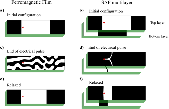
Comparison between current-induced motion of domain walls in ferro and antiferromagnetic materials. The red cross marks the location of a pinning center with 50% stronger anisotropy. Black (white) regions indicate areas where the out-of-plane component of the magnetization is positive (negative). The initial configuration in the ferromagnetic and antiferromagnetic systems are shown respectively in (a, b). We start by ramping an in-plane magnetic along the bar direction up to Hx = 0.9 T. As soon as the field reaches its maximum, an electrical current pulse is applied for 20 ns. (c, d) show the domain configurations at the end of the electrical pulse. Finally, the relaxed domain states, once the electrical current and magnetic field are both switched off, are shown in (e, f).
In analogy to the experiment, an in-plane magnetic field is applied along the orientation of the bar, and its magnitude is ramped from zero to Hx = 0.9 T. Once the field reaches the maximum magnitude, an electrical current is applied. In the SAF system the current density is j = 2 × 10⁷ A/cm2, similar in magnitude to the current pulses used in the experiment. The current pulse triggers domain wall propagation, which is then blocked by the pinning site. Like in the experiment, the pulse duration in the simulation has been long enough for the domain walls to come to a standstill before the end of the current pulse. The domain configurations at the moment the current is switched off are shown in c and d in the ferromagnetic and antiferromagnetic bars, respectively. Apparently, not only the pinning site affects the motion of the domain wall but, the stray fields generated by the domains in the ferromagnetic bar also have a strong and long-range influence on the domain wall motion resulting in a complex stripe domain structure. On the other hand, in case of the antiferromagnet, domain wall motion is prevented only locally by the pinning center. Eventually, the equal helicities of the twisted domain walls within the ((hat{{{{bf{z}}}}},hat{{{{bf{n}}}}})) plane, where (hat{{{{bf{n}}}}}) is the domain wall normal and (hat{{{{bf{z}}}}}) is along the easy-axis (supplementary Fig. S8b), prevents the antiferromagnetic domain walls from merging. Therefore, the walls can approach each other until the exchange penalty prevents them from moving any further.
Finally, e and f show the relaxed domain states after the electric pulse and the magnetic field have been switched off. The final states contain again only straight domain walls since the domain wall energy is minimized in both ferromagnetic and antiferromagnetic bars. While the final domain configuration in the ferromagnetic bar has been influenced by the global stray field, the antiferromagnetic domain configuration is determined only by the local pinning site where the domain wall remains located in its final position.
Our simulation considers only a single pinning site. In case of many pinning sites with normal distribution of depinning potentials, the critical current density for depinning domain walls and reversing correspondingly larger areas will simply follow an error function if individual and local depinning events are not correlated. Indeed, the experimentally detected degree of reversed antiferromagnetic domains versus writing current density follows an error function (dashed line in Figs. 1c and 6c).
Detecting the degree of reversed antiferromagnetic domains by measuring nonlinear magnetotransport response yields in rather small signals. An alternative detection strategy using a 3-terminal device is illustrated in Fig. 5a, where one of the ferromagnetic layers of the SAF forms part of a magnetic tunnel junction. The counter electrode of the tunnel junction then acts as a magnetic reference layer, so that the tunneling magnetoresistance (TMR) signal corresponds to the ratio between the reversed antiferromagnetic domains within the SAF structure. In fact, the implementation of the SAF-based antiferromagnetic memory within a TMR junction device might be a realization of a magnetic synapses directly attached to a spin-transfer-torque oscillator or a probabilistic p-bit device, where its synaptic weight controls the degree of spin polarization driving the oscillation or the fluctuation, respectively51,52,53. Another interesting approach is to replace the ferromagnetic reference layer with a reference SAF structure (Fig. 5b). This reference SAF remains fully polarized in a single domain state and is magnetically decoupled from the “free” SAF structure below. Such a fully antiferromagnetic analog memory with large magnitude TMR linear response readout would be “written” by spin-orbit torque-driven antiferromagnetic domain wall motion. Note that damping-like SOT-driven antiferromagnetic domain wall motion is possible also if the spin accumulation is generated only at one interface towards the SAF structure. The system containing two compensated SAFs exhibits zero or significantly smaller net magnetization compared to the device proposed in a, thus retaining the merits of a fully compensated zero-net moment system such as being more robust against external and self-generated field perturbations.
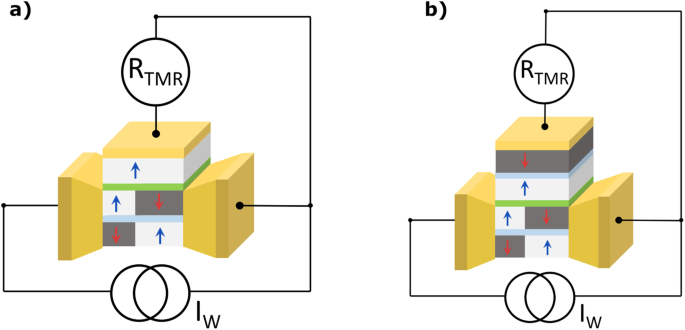
The nonlinear response yields a weak signal which does not favor its use in real applications. A possible alternative to probe the ratio between antiparallel states could be via a 3-terminal device, where the ratio would be translated into a tunneling current. The tunneling current can be measured across a single ferromagnetic layer (a) or a second synthetic antiferromagnet (b), which would preserve the zero net moment of the whole device.
Finally, it is worth mentioning that the analog antiferromagnetic memory may be also realized in real antiferromagnets or altermagnets where current-induced domain wall motion is expected. Indeed, spin-orbit torque-driven reproducible domain wall displacement of 90∘ and 180∘ domain walls has been observed in ({{{mathcal{PT}}}}) symmetric antiferromagnets44,45.
Methods
Electrical writing and reading
The experimental results were obtained on a 50 × 5 μm Hall bar, with an alternating probing current of 5 mA (RMS) and a frequency of 163 Hz. The longitudinal and transversal resistances detected at first and second harmonic frequencies are simultaneously measured. The first harmonic signal corresponds to the linear response of the current independent resistance. Whereas the second harmonic signal, or second-order response, measures the resistance contribution linearly dependent on the current amplitude. Detailed set of first and second-order data are presented in the supplementary Material sections 3 and 4.
We show simultaneously measured first and second-order responses in Fig. 6a. The two antiferromagnetic states can be clearly distinguished by the ({R}_{xx}^{2omega }) signals as long as an in-plane oriented magnetic field is applied. Prior to each of the four sweeps from zero to high field amplitude shown in Fig. 6a, an out-of-plane field pulse of ± 0.3 T was applied to set one of the two fully polarized antiferromagnetic states. By measuring only sweeps with increasing field strength, we avoided arbitrary switching to unknown magnetic configurations when crossing the in-plane spin flip field at ≈ 1.1 T, since the reversed antiferromagnetic states are energetically equivalent.
a Second harmonic signal, or nonlinear response, of the longitudinal contacts measured for an in-plane field sweep. In order to unambiguously set the magnetic state of the SAF, these sweeps were measured always starting from zero field after the application of out-of-plane ± 0.3 T to fully magnetize the whole sample with a particular antiparallel state. Instead of applying the out-of-plane field, a similar signal is obtained when an electrical pulse is sent through the sample at Hx = − 0.9 T. The antiparallel states are fully determined by the pulse polarity. b Linear response when measured after the positive (red line) and negative (blue line) pulses. c Comparison between the change in linear and nonlinear responses as a function of the pulse height. The dark dashed line is the result of fitting the data to a cumulative function of a Gaussian distribution, or error function.
In Fig. 6a, we compare the electrical switching with setting the antiferromagnetic states by the out-of-plane magnetic field pulses into a fully polarized state. Electrical current pulses of 1.83 × 10⁷ A/cm2 and 10 ms long were applied at Hx = − 0.9 T. Firstly, independently of the state set previously by the external field, the pulse’s polarity uniquely determines the antiferromagnetic state of the sample. Secondly, the nonlinear ({R}_{xx}^{2omega }) measurements indicate that the memory becomes fully polarized into a single-domain state after the application of a large electrical pulse.
It is also worth mentioning that probing ({R}_{xx}^{2omega }) with the external field along the current direction (x-axis) has the advantage that thermal effects, such as the anomalous Nernst effect and the spin-Seebeck effect, do not contribute to the measured signal (see Supplementary Material section 4). In Fig. 6b, c, the linear response of the longitudinal resistance comprises only the anisotropic magnetoresistance and the giant magnetoresistance, and therefore does not discriminate between reversed AFM states. This is confirmed in Fig. 6b, where both reversed antiferromagnetic states give equal responses. Furthermore, Fig. 6c highlights the independent nature of the linear response to different multilevel states, indicating that the memory always remains in a compensated antiferromagnetic regime.
Micromagnetic simulations
We performed micromagnetic simulations in order to study the domain walls in single ferromagnetic layer and in the SAF case. Specifically, how a magnetic domain wall propagates when affected by pinning centers and stray fields. The simulations were carried out using Mumax3 software. The simulation cover an area of 0.5 μm × 2μm discretized into 2048 × 512 × 3 and 2048 × 512 × 1 number of cells, for the SAF and FM cases, respectively. We considered a SAF comprising identical ferromagnetic layers, sharing their physical constants. We used a saturation magnetization Ms of 1.422 × 10⁶ A/m and a Gilbert damping of 0.1. The antiferromagnetic coupling strength and the uniaxial anisotropy were adjust to fit the experimental data, namely, both the spin-flip fields along and perpendicular to the easy axis. The antiferromagnetic coupling is set to 0.2 T and the perpendicular anisotropy to 1.96 × 10⁶ J/m3. A spin Hall angle of 0.15 was assumed.

Responses