Backward wave optical parametric oscillation in a waveguide

Introduction
Integrated nonlinear optics offers transformative advancements across various applications such as classical and quantum optical communications, signal processing, and photonic quantum computing1,2. This is made possible by the potential to develop miniaturized compact devices, seamlessly integrated with existing photonic platforms, which enhance the efficiency of nonlinear processes through the high intensities facilitated by intrinsic electromagnetic field confinement and extended interaction lengths3,4. Quasi-phase matching (QPM) is especially interesting for nonlinear integrated photonics because of the flexibility in tailoring nonlinear optical processes, offering the capability for designing spectral, temporal, spatial, and polarization properties of the generated radiation. QPM’s advantages have been extensively studied lately, particularly in quantum optics applications where ultrahigh efficiency devices were demonstrated5,6.
The QPM technique utilizes periodic modulation of the nonlinearity with a period Λ to compensate for the process’ phase mismatch, denoted by (Delta k=,mfrac{2pi }{varLambda }), where m represents the order parameter7. Most often, the modulation is performed by reversing the spontaneous polarization in ferroelectrics such as LiNbO3 or KTiOPO4 (KTP). While early research primarily focused on QPM waveguides in LiNbO38,9, van der Poel et al. demonstrated that segmented KTiOPO4 (KTP) waveguides offered a promising alternative due to improved overlap between interacting modes and higher power handling capabilities10,11. In segmented waveguides, ion-exchange induces the ferroelectric domain reversal, automatically forming the QPM structure. For a comprehensive overview of this topic, see ref. 12.
The Backward Wave Optical Parametric Oscillator (BWOPO) is a down-conversion device, with one of the generated waves propagating counter-directionally to the pump while the other travels co-directionally. Unlike a conventional Optical Parametric Oscillator (OPO) where all three waves interact in a co-propagating geometry, and which has to rely on external feedback through an optical cavity, the BWOPO automatically establishes distributed feedback due to the inherent counter-propagating nature of the nonlinear interaction. The lack of a physical cavity is particularly enticing for integrated nonlinear photonic applications, as it offers an inherent oscillator with a controllable spectrum. Additionally the absence of a cavity endows the BWOPO with robustness, ease of alignment, and high efficiency in a single-pass configuration, all within a compact footprint. Conversion efficiencies exceeding 70% and outputs at the mJ level have recently been achieved in bulk devices13.
The BWOPO presents markedly distinct spectral characteristics compared to the conventional OPO. The forward wave retains the spectral width and phase of the pump, whereas the backward-generated wave inherently exhibits a narrow spectrum14,15,16. Until now, pulse energies of several µJ or more were required to initiate a BWOPO. However, using a waveguide can significantly lower this threshold, allowing for the use of lasers with low pulse energy. This advancement will enable the development of ultra-compact, robust, cost-effective, narrowband near- and mid-infrared sources. The exceptional spectral attributes are also garnering significant interest within quantum optics applications as they enable the generation of high-purity and narrowband heralded single photons17,18,19. In co-directional spontaneous parametric down conversion (SPDC), there is a trade-off between the photon pair generation rate and the spectral bandwidth of the entangled photons. In type-0 phase matching, where all photons share the same polarization, the generation rate is the largest but produces broadband photons typically spanning several THz. To generate narrowband entangled photons, typically, either filters are employed or a phase matching scheme where the down-converted photons have orthogonal polarizations, so called type-2 phase matching, is used. Yet, both options significantly reduce the photon generation rate. Counter-propagating SPDC eliminates this trade-off by allowing the use of type-0 phase matching, which results in higher photon pair rates and a narrower emission spectrum compared to type-2 phase matching. Furthermore, despite the absence of the filtering effect typically provided by a cavity, a high level of squeezing, comparable to that achieved by conventional OPOs, should be attainable when a BWOPO is operated in the proximity of the oscillation threshold20. A guided wave version of the BWOPO will provide intriguing new possibilities to the integrated optics tool box.
The antiparallel propagation of signal or idler photon with respect to the pump introduces a large phase-mismatch:
where k is the wavevector, Λ is the periodicity of the QPM structure, m the phase matching order and the subscripts p, f, and b denote pump, forward and backward waves, respectively. For the same wavelengths of the interacting waves, the phase mismatch Δk for counter-propagating interaction is about two orders of magnitude larger than that for the co-propagating one. This large phase mismatch makes QPM the sole viable method for satisfying the phase-matching condition. In most-developed ferroelectrics such as LiNbO3, LiTaO3, or KTP, poling periods below 1 µm are required for first-order (m = 1) QPM interactions. However, fabricating such fine-pitched structures presents a formidable challenge, which significantly delayed the first experimental BWOPO demonstration21. Recent advancements14,22 have shown that the limitations in fabrication can be surmounted through coercive field engineering in rubidium-doped KTP (RKTP), allowing consistent fabrication of bulk sub-µm domain gratings with periodicities presently down to 317 nm23. This method utilizes ion exchange to establish alternating regions with low and high coercive fields, enabling polarization reversal through electric field poling using planar electrodes.
Counter-propagating photon pair generation has recently been demonstrated in waveguides with periodicities of 1.7 µm24 and 1.3 µm25. These devices were based on fifth-order (m = 5) and third-order (m = 3) QPM, which proportionally reduced the effective second-order nonlinearity,(,{d}_{{eff}}={2d}_{33}/(pi m)) while the oscillation threshold would increase by 25 or 9 times, respectively. Oscillation was consequently not achieved in these waveguides. Currently, the most efficient KTP QPM waveguides are fabricated by first implementing the QPM grating through electric field poling, followed by waveguide inscription via ion exchange12. However, the finely pitched ferroelectric domains required for realizing BWOPO are susceptible to back-switching at the high temperatures used for waveguide fabrication26, which has hindered the development of waveguide BWOPOs.
In this study, we introduce sub-micrometer (Λ = 409 nm) periodically poled RKTP waveguides and use them to demonstrate the first-ever waveguide-based BWOPO. The waveguides were fabricated on the polar surface of an RKTP crystal utilizing a two-step process. Initially, a segmented ion-exchanged periodic structure was formed, serving as waveguides and a coercive field grating. Subsequently, the QPM grating was inscribed via electric field poling, eliminating the need for subsequent heat treatment. This approach enabled precise control over the first-order QPM structure within the waveguides, paving the way for the realization of waveguide BWOPOs with unprecedented performance characteristics.
Results
The PPRKTP waveguides were 22 mm long with a QPM grating length of 20 mm. They were characterized in the setup shown in Fig. 1. A Ti:Sapphire regenerative amplifier was used as the pump source, providing linearly chirped pulses with a duration of 215 ps and a chirp rate of 19.4 mrad/ps2, at a repetition rate of 1 kHz. The pulses had a center wavelength of 798.9 nm and a spectral bandwidth of 1.0 nm (470 GHz). A waveplate-polarizer arrangement was employed to regulate the launched pump energy and ensure polarization alignment along the crystal’s polar axis, thereby exploiting its d33 coefficient. The light was introduced into the waveguide through an objective lens (Melles Griot, 06 GLC 003) with a focal length of 8.48 mm and a numerical aperture (N.A.) of 0.28. Subsequently, the light exiting the waveguide was collected using a second objective lens (Melles Griot, 06 GLC 001) with a focal length of 1.21 mm and an N.A. of 0.61. Dichroic mirrors positioned before and after the waveguide were used to separate the pump from the down-converted light. Transmission measurements below the oscillation threshold reveal 92% waveguide transmission over a length of 22 mm for the pump, which corresponds to a low loss of 0.2 dB/cm, similar to the loss values achieved in ref. 27.

HW half-wave plate, POL polarizer, DM dichroic mirror, LPF long-pass filter, PM power meter, OSA optical spectrum analyzer, PPRKTP periodically poled RKTP sample.
The BWOPO threshold was reached in 50 out of the 55 waveguides present in the sample (see Methods). We opted to conduct a more comprehensive investigation of a waveguide with a width of 9.8 µm. For this waveguide, the BWOPO threshold was reached for a pump energy of 325 nJ, corresponding to an average power of 325 µW and a peak power of 1.51 kW. That represents a remarkable 19-fold reduction when compared to recent bulk BWOPO experiments conducted with the same laser used as pump source28. Figure 2 displays the spectra of the forward and backward waves recorded at pump energies corresponding to twice the oscillation threshold. To facilitate comparison, the spectra obtained from a bulk sample featuring the same QPM period are presented. Owing to waveguide dispersion effects, the central wavelength of the backward, signal wave shifted from 1511.7 nm in the bulk sample to 1514.6 nm in the waveguide. Similarly, the central wavelength of the forward, idler wave shifted from 1692.8 nm in the bulk sample to 1688.7 nm in the waveguide. The QPM condition for the signal backward generating BWOPO in the waveguide, ({k}_{p}+{k}_{b}-{k}_{f}-{K}_{g}+varDelta {K}_{w}=0,) takes into account the additional phase mismatch, (varDelta {K}_{w}) due to waveguide dispersion. The observed spectral shift in the waveguide implies that (varDelta {K}_{w}=+3.75cdot {10}^{-2}mu {m}^{-1}). The observed spectra display the hallmark characteristics of a BWOPO. Here, the spectral phase of the pump is transferred to the forward wave, leading to the generation of a broad spectrum spanning 98 GHz. Conversely, the backward wave is spectrally much narrower, with a bandwidth of 21 GHz.
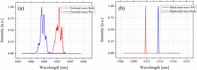
Forward (a) and backward (b) wave spectra at pump energies twice the oscillation threshold generated in waveguide and bulk, respectively.
Figure 3 illustrates the output energy of the parametric waves and the internal conversion efficiency as a function of pump energy. The backward wave energy was directly measured, while the forward wave’s energy was determined using the Manley-Rowe relations. At a pump energy of 714 nJ, a peak conversion efficiency of 8.4% was observed. However, the BWOPO efficiency declined at larger pump energies due to the emergence of backward stimulated polariton scattering (BSPS). In PPRKTP, BSPS is known to be a very efficient nonlinear process that can compete with quasi-phase-matched nonlinear processes29. The QPM grating suppresses forward polariton scattering but not BSPS, which is produced by large-momentum slow polaritons. The slow polaritons reside close to the polar TO-phonon resonances, therefore they do not experience the χ(2) modulation in PPRKTP before absorption takes over. In fact, the first BWOPO demonstration in a bulk crystal suffered from limited conversion efficiency for the same reason21. In a well-poled bulk PPRKTP sample, the parametric nonlinear interaction exhibits a substantially lower threshold and depletes the pump before the onset of BSPS. That recently allowed reaching a record 70% efficiency in bulk BWOPO devices13. However, when employing an imperfect QPM grating, the effective nonlinearity for the three-wave-mixing process is diminished. Consequently, BSPS can compete with BWOPO and limit the achievable efficiency. Additionally, for a waveguide the modal overlap area, ({A}_{{ovl}},) is an important parameter, as the pump power at threshold scales as ({A}_{ovl}/{({d}_{eff}L)}^{2}), where L is the waveguide length.
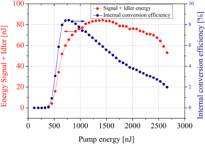
Internal conversion efficiency and energy of the parametric waves as a function of the pump energy.
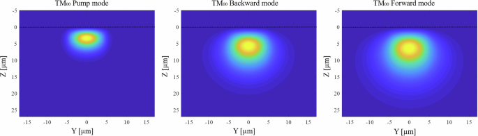
To investigate the mode overlap, we simulated the TM00 mode profiles of the pump-, backward-, and forward-waves for the waveguide (see Methods). Their intensity distribution are shown in Fig. 4. It can be seen that the intensity maximum pushed deeper into the bulk for longer wavelengths at the same time as the mode gets larger. With such suboptimal field overlap, the nonlinear interaction is reduced. We calculate the overlap area as:
where ({E}_{p}), ({E}_{b}) and ({E}_{f}) are the normalized electric field distributions of the pump, backward and forward modes, respectively, while the transversal coordinates y, z correspond to the crystal indicatrix axes. Notably, an increased field overlap would result in a smaller effective area and a lower BWOPO threshold. Utilizing the electric field distributions obtained from the simulation and applying them to Eq. 2 results in an effective area of 296 µm2. Substituting this value into the BWOPO threshold expression for pulsed pumping, derived in ref. 30, we ascertain an effective nonlinear coefficient, ({d}_{{eff}}=3.5,frac{{rm{pm}}}{{rm{V}}}) (ideally 10.8(,frac{{rm{pm}}}{{rm{V}}}) in PPKTP31). It shows that the quality of the QPM structure can be further improved (see Fig. 5 and Methods). A second avenue for improvement involves increasing the modal overlap, which could be achieved by using buried waveguides. One feasible approach might entail employing a secondary ion exchange process in a KNO3 melt to reverse the effects of the initial exchange at the top layer, similar to the reverse proton exchange technique utilized in LiNbO332 and LiTaO333. Improvements in this context could involve identifying an ion exchange procedure that creates a large enough refractive index increase to ensure waveguiding while simultaneously preventing spontaneous domain reversal.
The dashed black line denotes RKTP surface positioned at z = 0, with the positive z-direction indicating the bulk and the negative z-direction representing air.
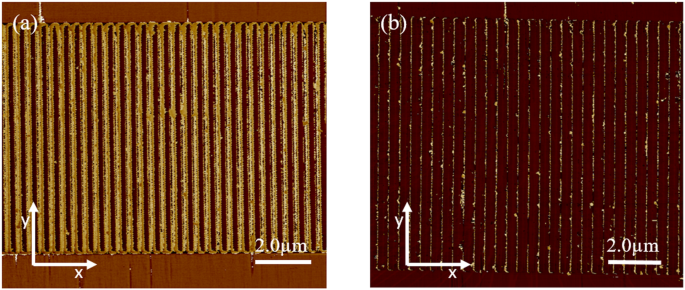
The x-axis represents the direction of light propagation. In (a) only the electric field poling inverted the polarization. In (b) the polarization was inverted via electric field poling and ion exchange.
In summary, we have presented a method to fabricate QPM waveguides in RKTP with a poling period well below 1 µm. The waveguides exhibited low loss (0.2 dB/cm) and were used to demonstrate the first-ever waveguide BWOPO. The backward signal wave had a wavelength of 1514.6 nm and a linewidth of 21 GHz, while the forward idler wave appeared at 1688.7 nm with a linewidth of 98 GHz, replicating the pump. The BWOPO threshold was 325 nJ, more than 19 times lower than what has been obtained in bulk samples. The conversion efficiency was limited to 8.4% due to an onset of BSPS. The BWOPO threshold in PPKTP waveguides can be further reduced by about 20 times in the same waveguide geometry by exploiting longer samples and by increasing the quality of the QPM structure so that the maximum deff could be exploited. It would reduce the pump pulse energy and peak power at threshold to about 15 nJ and 70 W, respectively. That would put the BWOPO waveguide technology in the realm of mode-locked laser oscillators as well as compact narrowband gain-switched fiber and solid-state lasers34,35. The unique spectral features of counter-propagating down-conversion should allow for the generation of high-purity and narrowband single photons in a ready for integration package, offering exciting prospects in applications such as photoacoustic spectroscopy, molecular spectroscopy as well as in quantum technologies. This waveguide fabrication method used should be scalable to even shorter periods, enabling down-conversion of both signal and idler counter-propagating to the pump – a nonlinear interaction that has not yet been demonstrated.
Methods
QPM waveguide fabrication
To fabricate the QPM waveguides, a 24 mm long RKTP sample was initially patterned on the c–-surface using UV-interference lithography, creating a photoresist grating with a 409 nm period. Following this, an ion exchange stop layer was introduced within the openings of the photoresist by exposing the patterned surface to oxygen plasma etching36. Subsequently, the remaining photoresist was removed, and the same surface was patterned with a waveguide design using conventional photolithography, forming channels along the x-direction with widths ranged from 6 µm to 22 µm. The RKTP surface was then subjected to oxygen plasma etching once more.
Following this preparation, ion exchange was carried out by immersing the crystal into a molten salt bath containing 20 mol% KNO3, 73% RbNO3, and 7 mol% Ba(NO3)2 at a temperature of 330 °C for 4 h. This ion exchange recipe, well-studied for electric field poling via coercive field engineering, led to the formation of segmented ion exchanged channels serving both as waveguides and coercive field gratings. In the final step, the segmented structure was periodically poled by contacting the two polar surfaces with planar liquid electrodes and applying 1.25 ms long pulses of 8 kV.
Figure 5 shows piezoelectric force microscopy (PFM) images of two representative parts of the ferroelectric domain structure for a 10 µm wide waveguide. In Fig. 5a the polarization is inverted in the non-exchanged areas only, resulting in a nearly ideal QPM structure with 50% duty cycle. However, in part of the waveguides, the ferroelectric domain structure was overpoled, as illustrated in Fig. 5b. We attribute this imperfection to two independent mechanisms: electric field poling in the non-exchanged regions and spontaneous domain reversal in the ion exchanged regions during the ion-exchange process. The latter is a well-known effect that occurs during certain ion exchange conditions. This was exploited in the original method for making QPM waveguides in KTP10. In the parts with combined spontaneous and electric field induced domain reversal only approximately 40 nm thin domains remained unaltered, as can be seen in Fig. 5b. To obtain further insight into the ferroelectric domain structure, a second sample was processed with the same recipe as described above, but patterned with a period of 580 nm. After poling it was polished and scanned with the PFM, see Fig. 6. At the top of the sample, domains inverted during ion exchange exhibit a cone-shaped structure, with depths ranging from 3 µm to 6 µm. Between the ion exchange regions, domains were inverted via electric field poling, maintaining their width for approximately 25 µm before merging. A similar behavior has previously been reported in ref. 22.
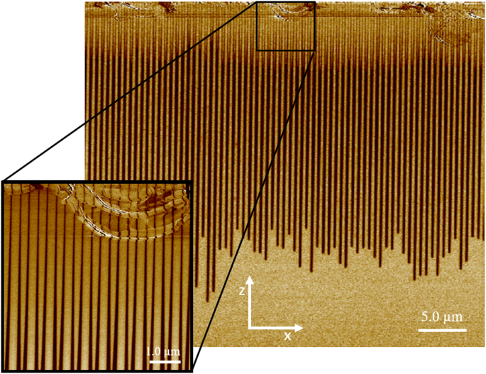
The z-axis represents the polar axis of the crystal, while the x-axis indicates the direction of light propagation. The domains inverted by electric field poling propagate approximately 25–30 µm into the bulk before they merged. The depth of the domains inverted by ion exchange exhibit cone-shaped structures with depths ranging from 3 to 6 µm, as shown in the inset.
Waveguide mode simulation and model calibration
The mode profiles were simulated using the wave optics module in COMSOL. Ensuring the accuracy of these simulations required precise refractive index data. For that reason, we subjected a single-domain reference RKTP sample to planar ion exchange using the same recipe as for the segmented waveguides. Energy dispersive X-ray spectroscopy was employed to determine the exchange profile. As expected, the Rb+-ion concentration follows a complementary error function37, with an erfc(z)-depth of 13 µm. The refractive index change for the planar waveguide was measured using prism coupling38 with a He-Ne laser at 633 nm. The surface refractive index increase was calculated to be 0.0064 using the inverse Wentzel-Kramer-Brillouin method39. Given that the BWOPO waveguides are segmented with a duty cycle of ~50% the surface refractive index change for the waveguides was modeled as half of the measured value of the planar waveguide.


Responses