Biomimetic freestanding microfractals for flexible electronics

Introduction
Learning from nature offers valuable insights for developing new materials and designs, inspiring bioinspired materials with special functionalities that are gaining significant attention in engineering research1. Scientists draw inspiration from the unique microstructures of functional biological materials, leading to innovations across various applications, including microfluidics2, water-oil separation3, anti-biofouling4, cell culture5, water harvesting6, and heat transfer7. These biological surfaces have evolved to achieve “intelligent adaptive functionality,” revealing unique topographies, functionalities, and surface chemistries applicable to numerous fields1,8,9. Notable examples include biomimetic superhydrophobic and photonic microstructures enabling next-generation heat transfer and optoelectronics applications10. In addition, the remarkable ability of biological systems to sense and adapt to complex environmental conditions has inspired the design of next-generation electronics with advanced functionalities. Emerging bioinspired strategies are now being applied to develop flexible and stretchable electronics that can accommodate mechanical deformations and seamlessly integrate with biological systems11,12.
Among the bioinspired architectures, fractal structures have been reported to provide greater stability and extensive surface coverage7,12,13, paving the way for advancements in efficient energy harvesting14, energy storage15, and flexible electronics16. Additionally, their properties can be integrated into modern electronics to address various challenges in the electronics and healthcare industries, offering advanced electronic functions and compliant mechanics12. Fractal-like structures have the unique ability to enhance surface area, improve stability, and efficiently manage the transport of electrical and thermal energy13. These patterns, inspired by nature’s inherent designs such as snowflakes and leaf skeletons, offer a high surface area-to-volume ratio compared to conventional flat surfaces, which is crucial for applications requiring efficient energy collection and transfer, such as photovoltaic cells17, sensors18,19, and antennas20. Additionally, the self-repeating nature of fractal designs provides numerous charge-transfer paths and supports higher loading of functional materials like metal nanowires, thereby maximizing electrical conductivity7. The creation of these fractal structures can be achieved through advanced fabrication techniques such as lithography-based approaches and precise modeling, or by directly utilizing naturally abundant materials that already exhibit these complex patterns11. Current technologies in nanopatterning substrates include research based on kirigami structures21,22, Peano curves23,24, Greek crosses25,26, Vicsek fractals27 and many other types of fractal constructs. These designs enhance functional properties such as stretchability, transparency, and breathability within the flexible electronics domain.
In our previous studies, we reported a range of fractal structures based on leaf skeletons that can be utilized for different applications. Unlike artificially designed fractal constructs, leaf skeletons naturally provide hierarchical, multiscale architectures that simultaneously optimize mechanical flexibility, breathability, and transparency. Their inherent structural efficiency enables enhanced electrical and thermal energy transfer, while their scalability and ease of preparation as biotemplates simplify the fabrication process at the miscroscale. For example, these fractals can be coated with different functional materials like Cu, CuO, for excellent water-harvesting surfaces28. For flexible electronics applications, these fractals can be covered with nanowires to achieve excellent conductive surfaces that are very flexible and transparent. These conductive surfaces can be used as electrodes in tactile sensors to fabricate e-skins19 and as biopotential signal measurement electrodes12 as demonstrated in our previous works. In addition, the fractal-like architecture aids in efficient heat transmission and was used in the fabrication of flexible thermotherapy patches7. The above-mentioned proof-of-concept studies demonstrated various functional properties such as high uniformity, transparency, flexibility, and degradability. However, there were issues with the scalability of the surfaces, stretchability, and potential for industrial use. Additionally, due to the lignin content, the surfaces were less durable7.
To meet the growing demand for efficient, inexpensive, scalable, durable, and accurate replication of natural surfaces, novel approaches and techniques are required. Templating is a well-established and efficient method for replicating both micro- and nanostructures found on natural surfaces29. Among templating methods, soft lithography is a promising method for the mass production of polymer surfaces with complex micro- and nanoscale biomimetic structures, displaying high aspect ratios and high-precision replication30,31. This technique is well-suited for applications in plastic electronics, biotechnology, and the design of nonplanar surfaces32. Photolithography33,34, electron beam lithography35,36, and 2D photon lithography37 are also other techniques currently used to fabricate biomimetic surfaces for photonic and flexible electronics applications but are very slow and consume significant amounts of energy. Other techniques, such as printing, are also promising, but replicating 3D freestanding fractal patterns at the microscale remains challenging38. Printing nanopatterns on everyday electronics requires energy-intensive methods like lithography, additive manufacturing, roll-to-roll processing, and cleanroom facilities, demanding significant time and resources.
In this work, we present a novel biomimetic microfabrication technique to replicate freestanding leaf skeleton-based fractal surfaces. We utilized a modified electrospinning method, replacing the fiber collector with a metalized biotic collector to replicate the microstructures. The biotic collector, based on a real leaf skeleton, was coated with metal (Cu in this case) using a combination of physical vapor deposition and electrodeposition, as demonstrated in our previous studies28,39. A range of fibers can be electrospun on the biotic collector, and post-processing yields perfectly replicated and freestanding surfaces with a replication accuracy of ~90%. Combining the properties of biotic architecture and polymer characteristics, these biomimetic freestanding surfaces are transparent, breathable, and stretchable. The method is versatile, allowing for the use of a wide range of polymers in biomimetic microfabrication. The electrodes developed in this work were demonstrated as transparent and breathable electronic skin (e-skin). The biomimetic conductive fractal patterns (BCFP) were fabricated by immobilizing AgNWs using a simple spray-based method. The BCFP exhibited high conductivity with sheet resistances less than 20 Ω sq–1 while maintaining good transparency. The BCFP conformally attaches to human skin, acting as an e-skin. To demonstrate the application, the BCFP was used to fabricate a tactile pressure sensor. In addition to their good transparency at low sheet resistances, the BCFP also exhibited stretchability, moisture resistance, and tight conformal bonding with the target surface. These allow the evaporation of perspiration, making them suitable for long-term use as epidermal sensors. The application of BCFP in advanced biomimetic e-skin was demonstrated through gesture monitoring experiments.
Results
Figure 1a illustrates the biomimetic microfabrication of fractal surfaces using a modified electrospinning technique. This method, which is both straightforward and scalable, involves using electrospun polymer nanofibers to create micropatterns on a biotic template, enhancing its stretchability, transparency, breathability, and uniform conductivity.

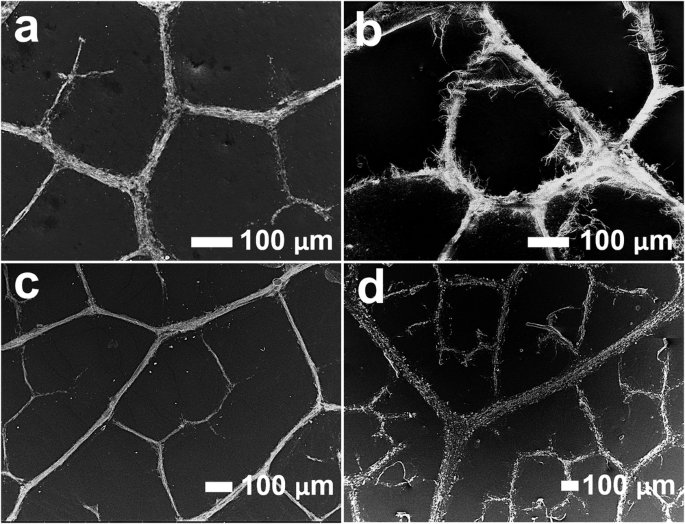
a Schematic of the replication process – metallic collector and optimized electrospinning unit. b Optical and SEM images of Ficus religiosa leaf skeleton: b1 represents the optical image, b2 and b3 represent the SEM images at different scale. c Optical and SEM images of biomimetic F. religiosa replicated surface: c1 represents the optical image, c2 and c3 represent the SEM images at different scale.
To prepare the customized electrospinning setup, the stock collector was replaced with a biotic collector, basically a metalized leaf skeleton (Supplementary Fig. 1). As detailed in the experimental section, the biotic collector was prepared using an electrodeposition process. When voltage was applied, fibers conformed closely to the intricate fractal structures of the biotic collector, resulting in freestanding biomimetic films with microfractals that could be easily peeled off for use in electrode fabrication. The targeted deposition replicates the natural microfractals in synthetic materials and enhances the functional properties of the resultant surfaces. Nylon 6 (N-6) was chosen as a model electrospinning polymer for its stiffness, abrasion resistance, excellent impact strength, wear resistance, and electrical insulating properties.
Two types of electric forces in the electrospinning process can influence the arrangement of electrospun fibers: the electrostatic force from the electric field and the Coulombic interactions between the positive charges on the nanofibers and the negative charges on the collector40. Compared to a plate collector, the electric field’s structure changes, causing the electrostatic forces to drive fibers toward the biotic collector. As the electrospun fibers approach the collector, Coulombic interactions between the opposite charges result in a preferential deposition of fibers on the metallic Cu layer of the microfractals41. This leads to a higher fiber density on the metallic microfractals than in the areas between the fractals.
To confirm the replication of the biomimetic fractal surfaces, Scanning Electron Microscope (SEM) characterization was conducted, and the SEM micrographs are shown in Fig. 1b2, b3 and c2, c3. These images display the natural fractal microstructures of leaf skeletons Ficus religiosa (sacred fig) alongside the replicated fractal microstructures at various scales. F. religiosa based biotic collector was used as a model system due to its unique fractal-like assembly of vascular bundles and peripheral interconnected fibers, which are visible in Fig. 1b, and its ease of processing as demonstrated in our previous works7. These fibers contribute to the mechanical stability and flexibility of the structure. Figure 1c2, c3 shows the SEM micrographs of the electrospun biomimetic patterns of F. religiosa using N-6. As evident from the SEM micrographs, the nanofibers were deposited onto the fractal architecture of the leaf skeletons, thus demonstrating a successful replication method. The optical images of the real leaf skeleton and the replicated surfaces were imposed onto each other using ImageJ and it showed ~90% replication accuracy.
Since the replication process is fiber-based, we considered dimensional accuracy to determine the replication accuracy. It is noteworthy to mention that due to the fiber-based deposition, no nanostructures are replicated as they would be in lithography. To assess the dimensional replication accuracy, we divided the leaf skeleton fractal patterns into different zones based on their hierarchical venations. Specifically, the biomimetic surface replicated from F. religiosa was used as the model substrate, with the metallic F. religiosa collector serving as the reference. As shown in Supplementary Fig. 2, Zone 1 represents the main midrib of the leaf skeleton; Zone 2 comprises the veins extending from the midrib; Zone 3 includes the branches originating from these veins; Zone 4 and Zone 5 consists of smaller fractal patterns as sub-branches emerging from the branches. Replication accuracy was evaluated by measuring the widths of the replicated biomimetic F. religiosa surface at multiple points within each zone (refer to Supplementary Fig. 2) and comparing these measurements with the corresponding features of the base metallic leaf skeleton. Based on this analysis, the replication accuracies for the replicated biomimetic F. religiosa surface at Zones 1, 2, 3, 4 and 5 were determined to be 78.7%, 86.3%, 90.1%, 95.6%, and 95.4%, respectively. These results highlight the precision of our modified electrospinning setup in replicating plant leaf microfractal structures, achieving an average replication accuracy of ~90% and demonstrating its reliability in producing high-quality microstructured biomimetic surfaces.
To demonstrate the versatility of the biomimetic method, the replication was also done on the leaf skeletons of Ligustrum lucidum (Chinese pivet), and Populus tremuloides (trembling aspen). These were chosen for their varying microfractal morphology and dimensions which significantly influence the surface’s mechanical and optical properties as highlighted in our previous studies13. These variations in microfractals and their length scales affect properties such as stretchability, transmittance, surface area, and processability13. Supplementary Fig. 3 contains SEM images of the control N-6 nanofiber mat, while Supplementary Fig. 4 includes SEM images of the replicated surfaces of F. religiosa, L. lucidum and P. tremuloides. Optical microscopic images of the control N-6 mat, and the biomimetic F. religiosa, L. lucidum, and P. tremuloides, are presented in Supplementary Fig. 5 to further compare the biomimetic designs with planar surfaces.
Depending on the application, different polymers with specific properties need to be used. This biomimetic microfabrication can be achieved using a variety of polymers. We conducted biomimetic electrospinning using four distinct polymers, and the results are presented in Fig. 2. The SEM micrographs display the replication of F. religiosa leaf architecture using Nylon 6 (N-6), Polyvinyl alcohol (PVA), Polyurethane (PU), and Polycaprolactone (PCL). These images demonstrate that the replication technique is effective across different polymers, achieving an average accuracy of ~90% in the case of N-6 in Fig. 2a, PU in Fig. 2c, and PCL in Fig. 2d. It is noteworthy to mention that, despite the successful replication achieved with PVA in Fig. 2b, the brittle nature of the material prevents the structures from maintaining their shape during the peeling process. The stretchability tests of replicated surfaces using four different polymers are shown in Supplementary Fig. 6. The stretchability results indicate significant variation in mechanical behavior depending on the polymer. For instance, PU exhibited the highest stretchability (~200%), while PVA showed the lowest (~7.5%). This variation is primarily due to the intrinsic mechanical properties of each polymer. For all polymers, the incorporation of the F. religiosa fractal structure enhances the stretchability compared to their planar control surfaces, as detailed in Supplementary Fig. 6b–e.
a Nylon 6 (N-6) based biomimetic surface. b Polyvinyl alcohol (PVA) based biomimetic surface. c Polyurethane (PU) based biomimetic surface. d Polycaprolactone (PCL) based biomimetic surface.
To evaluate the stretchability and mechanical stability of the biomimetic patterns, mechanical testing was conducted using a texture analyzer. Figure 3 presents the mechanical properties of electrospun biomimetic substrates composed of N-6 nanofibers and their corresponding micropatterns modeled after leaf skeletons. Each fractal micromesh design displays unique stretchability characteristics. The initial step involved determining the intrinsic stretchable properties of N-6 nanofibers as a control. This was achieved by electrospinning the polymer onto flat aluminum foil control surfaces to produce a planar control N-6 mat with the same thickness as the biomimetic surfaces. The stress-strain properties were assessed using a texture analyzer. To ensure consistent comparison, all nanofiber substrates were cut to specific dimensions (3 cm × 1.2 cm). Figure 3a shows stress-strain curves of the biomimetic patterns along with the control surface. As evident from the figure, the control planar substrate exhibits the lowest stretchability. In contrast, the biomimetic surfaces based on F. religiosa, L. lucidum, and P. tremuloides demonstrate enhanced stretchability. This improvement is attributed to unique fractal designs, that allow for increased stretchability by functioning like a bundle that binds the fibers together, thereby increasing both strength and stretchability. Experimental data indicates that among the bioinspired designs, the biomimetic surface based on F. religiosa exhibits the highest stretchability having strain tolerance up to around 38% as shown in Fig. 3a. Breaking strains for L. lucidum and P. tremuloides are around 28% and 34% which can also be seen in Fig. 3a. The observed differences in stretchability among the biomimetic surfaces are attributed to variations in the structural features of the leaf skeleton architectures. The F. religiosa surface exhibits the highest stretchability (~38%) due to its highly interconnected fractal patterns, which distribute stress more uniformly. In contrast, the denser, less interconnected structures of L. lucidum (~28% stretchability) and P. tremuloides (~34% stretchability) lead to localized stress concentrations, reducing flexibility13. The deviation between the predicted and experimental strain values arises from model assumptions, such as uniform material properties and perfect fiber adhesion, which do not fully account for microscale imperfections in the replicated surfaces42. The fibers in the replicated surfaces also shrink slightly due to post-heat treatment, contributing to microscale imperfections and the observed deviations between the predicted and experimental strain values.
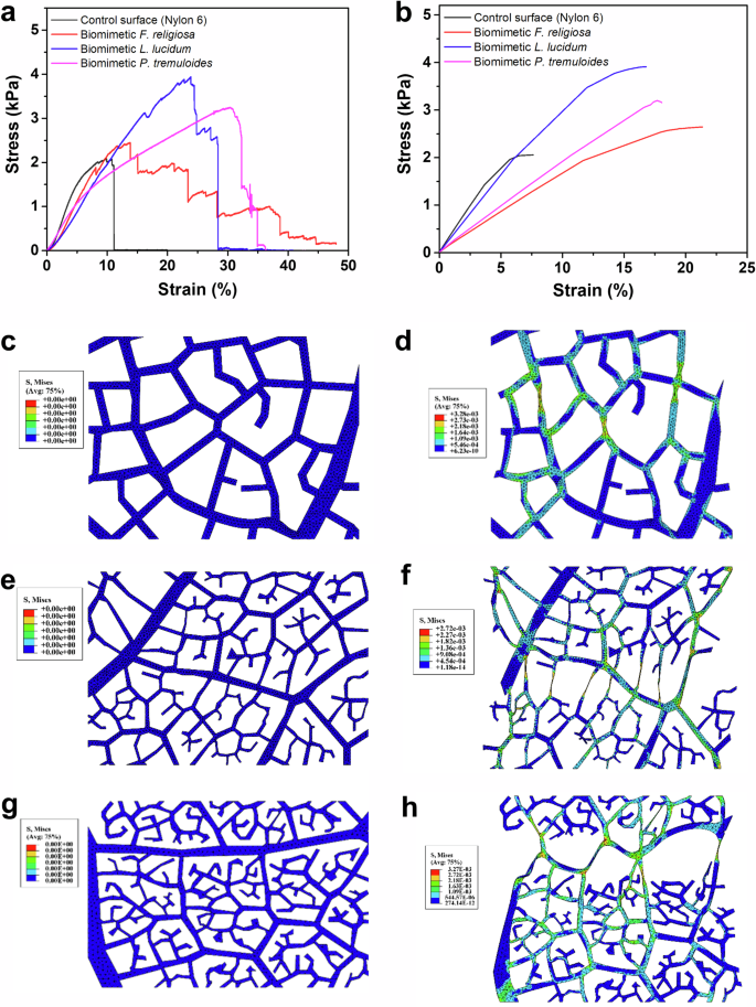
a Strain vs stress curve of the control surface and biomimetic surfaces of F. religiosa, L. lucidum, P. tremuloides using N-6 polymer. b Simulated result showing strain vs stress curve of the control surface and biomimetic surfaces of F. religiosa, L. lucidum, P. tremuloides. The deformation of the replicated surface. c The start of loading for L. lucidum biomimetic surface. d The deformation of L. lucidum biomimetic surface after 20% strain. e The start of loading for F. religiosa biomimetic surface. f The deformation of F. religiosa biomimetic surface after 20% strain. g The start of loading for P. tremuloides biomimetic surface. h The deformation of P. tremuloides biomimetic surface after 20% strain.
Figure 3b shows the predicted stress-strain curves of the control planar surface, and the biomimetic surfaces obtained from the theoretical model. The curves show similar results as they exhibit increased stretchability of biomimetic surfaces compared to the control surface. Figure 3c–h depicts the FEM analysis for the skeletons of L. lucidum, F. religiosa, and P. tremuloides, respectively. In all figures, the lower surfaces are fixed, and the upper surfaces are movable. Figure 3c, e, g shows the initial loading, while Fig. 3d, f, h display their deformation after being stretched upwards by 20% strain.
After the completion of the initial design phase, computer-aided design (CAD) models of three plant leaves, each with dimensions of 3 cm × 1.2 cm, were generated using SOLIDWORKS software. Subsequently, these CAD models were imported into ABAQUS software, and the procedures were replicated for the final structures. To compare the experimental results with the simulated results, a strain-stress diagram is provided for each sample Fig. 3a, b. The theoretical assumptions provided by the model are quite similar to the experimental results which show enhanced stretchability in the case of biomimetic surfaces. Upon comparing the diagrams, it is evident that the finite element method (FEM) results for the control surface (N-6 mat) display minimal deviation from the experimental results. In the FEM diagram (black line), the maximum stress is ~2 kPa at 7.5% strain, whereas the experimental diagram indicates a maximum stress of 2 kPa at around 9% strain, resulting in an error of ~15% for predicting the maximum deformation, with no error in maximum stress. By comparing the diagrams for F. religiosa (red lines), the highest stress is about 2.5 kPa at under 22.5% strain. However, the actual diagram indicates a maximum stress of under 2.5 kPa at ~15% strain. This leads to an error of roughly 30% when estimating maximum deformation. The strain-stress diagram for L. lucidum (blue lines) and P. tremuloides (pink lines) leaves varies slightly. The prediction for maximum stress is fairly accurate (under 4 kPa for L. lucidum and over 3 kPa for P. tremuloides), but there are noticeable errors in predicting maximum strain, with deviations of about 40% and 45% respectively. Although there are discrepancies in predicting maximum deformation, the overall trend is quite similar and acceptable, aligning well with the experimental results. One common difference between the stress-strain property of nanofiber mats and the replicated nanofiber surfaces is seen at the breaking point. When the breaking point is reached for the case of nanofiber mats, there is a sharp downfall of the stress which represents immediate tearing of the mats. Whereas, in the case of the replicated surfaces, the trend shows that it tears at different instances until it completely tears apart. This is another proof of the nanofiber ropes being in action to resist complete tearing at once thus increasing the tensile strength and stretchability.
Figure 4a shows the schematic of the fabrication procedure for the BCFP. After the biomimetic process, the freestanding surfaces were sprayed with AgNWs and then peeled off the biotic collector and mounted on a 3D-printed frame. The fractal microstructures facilitate uniform coating as the AgNWs adhere only to the replicated nanofiber-based fractal framework. Energy-dispersive X-ray spectroscopy (EDS) measurements, shown in Fig. 4c, support this statement, demonstrating that the AgNWs are deposited solely onto the replicated fractal architecture, forming an identical pattern. Further justification is provided by an SEM image, which visibly shows AgNWs binding to the nanofiber ropes. The elements carbon (C) and oxygen (O), which are the main constituents of the biomimetic surface (N-6), and silver (Ag) are evident from the EDS spectrum Fig. 4d.
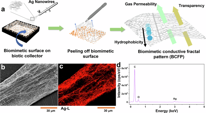
a Schematic of fabrication of BCFP with F. religiosa replicated surface. b SEM image of BCFP with AgNWs. c EDS mapping of the BCFP showing AgNWs decorated N-6 nanofibers. d Corresponding EDS spectrum of the BCFP based on biomimetic F. religiosa surface.
The conductivity of biomimetic BCFP with N-6 and F. religiosa architecture was tested with varying AgNW loadings shown in Fig. 5a. As the AgNW concentration increases, the sheet resistance decreases as expected. The uniformity of the sheet resistance was verified by measuring the sheet resistance at different positions along the X–Y axis on the replicated surface. The conductivity mapping of the surface (3 cm × 3 cm) is shown in Fig. 5b.
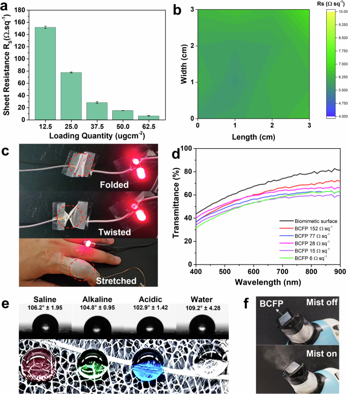
a Loading quantity of AgNW vs Sheet resistance experiment on F. religiosa replicated surface with N-6. Three independent measurements were conducted, and the error bars represent the standard deviation. b Conductivity mapping after AgNW loading on biomimetic F. religiosa surface. c The BCFP surface functioning as a conductor to light up an LED in folded, twisted, and stretched conditions having conformal skin attachment. d Transmittance studies of the biomimetic F. religiosa surface with varying quantities of AgNW loading. e Contact angle measurement and digital photographs showing droplets maintaining a spherical shape on the replicated BCFP surface, with red indicating saline water, green for alkaline, blue for acidic, and colorless for water. f Breathability test: digital images showing the BCFP allowing cool mist from a humidifier to pass through.
The biomimetic BCFP surfaces can freely adapt to skin deformations while consistently maintaining its conductive properties, even when the skin is folded, stretched, or twisted. To assess the impact of these deformations on the conductivity of the BCFP surfaces, a conductive path for lighting up an LED was tested. Figure 5c demonstrates that various conditions such as folding, twisting, and stretching have minimal effect on the BCFP’s conductivity.
One of the properties predicted to be enhanced in replicated surfaces compared to control surfaces and most electrospun surfaces is optical transmittance. The biomimetic surface exhibits higher transmittance due to the fractal surfaces of the leaf architecture. In one of our previous studies, we reported that the unique fractal orientation, surface coverage, and microstructure affect the optical transparency of electrodes based on leaf skeletons. Additionally, the fractal surfaces maintain transparency even with an increase in the concentration of NW in the solution. Figure 5d shows the transmittance spectra of the BCFP surfaces (2 cm × 2 cm) with different AgNW concentrations. The biomimetic surface (without AgNW) exhibits better transparency (>82%) compared to the planar control surfaces, as shown in Supplementary Fig. 7. While the transparency of the BCFP decreases slightly with increased AgNW loading, it remains above (55–65%) even at higher concentrations, highlighting the benefit of the fractal architecture7 in maintaining optical clarity. This trend contrasts with mat-like electrospun surfaces, which experience a sharper decrease in transparency as conductivity increases. The transparency of the BCFP can be enhanced even at higher concentrations by optimizing the NW spraying methods and using shorter NWs that adhere well to the replicated fractals without forming dense networks.
The conductive replicated surface must withstand harsh environments such as humid, acidic, and alkaline conditions. In addition, these should also possess anticorrosion properties that are typically achieved using encapsulating layers or coatings12. To enhance the BCFP surface’s durability under various conditions, we sprayed it with a hydrophobic solution (OrganoTex Spray-On) as a passivation layer (Supplementary Fig. 8). Additionally, AgNW-based electrodes are prone to surface oxide formation, which can affect their shelf life. Applying a hydrophobic layer can prevent oxidation while maintaining excellent surface conductivity. Notably, the resistance of the BCFP surface (~20 Ω sq⁻¹) was not affected after applying the hydrophobic layer (Supplementary Fig. 8). The BCFP surface exhibited good hydrophobicity, as saline water, alkaline, acidic, and neutral water droplets maintained a spherical shape on its surface shown in Fig. 5e. To quantify the hydrophobicity, we measured the static contact angles of saline water, alkaline, acidic, and neutral aqueous droplets on the hydrophobic BCFP surface, which were found to be 106.2°, 104.8°, 102.9°, and 109.2°, for saline water, alkaline, acidic and neutral water solution, respectively. The high contact angles indicate the hydrophobic nature of the BCFP surface, which can prevent water penetration. To evaluate the hydrophobic layer’s effect on BCFP durability, we placed BCFP surfaces (with and without the hydrophobic layers) in saline, alkaline, acidic and neutral water solution. At intervals over 1–7 days, the surfaces were removed from these solutions, and their resistance was measured. Due to their hydrophobicity and a small amount of air trapped within the skeleton, the surfaces floated on these solutions. The hydrophobic BCFP surfaces exhibited minimal changes in resistance even after 7 days of exposure to these harsh aqueous environments, indicating enhanced stability and durability (Supplementary Fig. 9a). In contrast, uncoated surfaces showed significant resistance changes over time, likely due to oxidation of AgNWs on their surfaces (Supplementary Fig. 9b). These results show that the hydrophobic layer effectively prevents aqueous solutions from penetrating the BCFP surface and significantly enhances its durability in harsh environments. Durability can be improved by using intrinsically stable, corrosion-resistant nanowires, such as gold or copper-nickel alloys, which resist oxidation and may provide long-term stability without any passivation layers.
The strong Van der Waals forces of the nanofibers enable the BCFP to adhere tightly to various surfaces, including natural skin. Its porous structure allows for air transmission, enabling sweat evaporation, making it ideal for long-term use as an epidermal electrode. Breathability is crucial for conducting surfaces, especially in healthcare and similar applications. Although the gravimetric (dish) method to determine water vapor permeability could not be used due to the micromesh architecture, we demonstrated water vapor transmission by placing the surface in front of a commercial humidifier generating a fine cool mist. The open micromesh structure of the BCFP creates large gaps that allow convective flow of water vapor and air, making traditional gravimetric methods unsuitable for accurate breathability measurements. Instead, the qualitative demonstration using a commercial humidifier (in Fig. 5f) effectively showcases the material’s capability to transmit water vapor freely through its porous architecture. As shown in Fig. 5f, the vapors pass through the BCFP, confirming its breathability. To assess the influence of humidity on the surface’s conductivity, we measured electrical conductivity after exposing the surface to a cool mist for 30 min. Notably, humidity had little effect on electrical conductivity. Even at very high humidity levels (>90%) and prolonged exposure, the resistance increased only slightly by 10%, which is acceptable and can be improved with different conducting materials. These results demonstrate the excellent stability of the BCFP’s electrical conductivity in a moist environment.
To assess the performance of the BCFP surface based on F. religiosa as a semi-transparent, stretchable, and conductive surface for e-skin applications, we integrated it into an LED circuit and evaluated its functionality during finger extension and flexion movements. The conductivity of the BCFP surface remained stable, as indicated by the constant brightness of the LED (refer to Fig. 5c and Supplementary video V1 in the supplementary files).
To further validate its performance, we measured the resistance changes of BCFP under varying strain conditions using a texture analyzer coupled with an LCR meter. The resistance exhibited a slight increase from 7 Ω at 0% strain to 17 Ω at 35% strain, demonstrating the conductive surface’s excellent strain tolerance (Supplementary Fig. 10). This small variation in resistance is attributed to the conductive fractal patterns of the BCFP surface, which effectively distribute mechanical stress, thereby preventing localized strain concentrations on the conductive surface. In comparison to previously reported planar conductive surfaces43,44, the BCFP surface maintains uniform conductivity even under repeated or significant deformation. These characteristics make the BCFP surface particularly well-suited for e-skin applications, where reliable and stable conductivity is critical under dynamic mechanical conditions, including repeated folding and bending.
The overall performance of the BCFP surfaces, fabricated using a biomimetic F. religiosa surface, featuring high transmittance (~82%), low sheet resistance (~20 Ω sq⁻¹), good breathability, device performance under stretching (~35%), and chemical stability (in saline, alkaline, acidic and neutral solutions for 7 days), was compared with current state of the art AgNW-based transparent electrodes45,46,47 and other structurally different electrodes reported in the literature (Supplementary Table 1). The comparative studies concluded that our BCFP surfaces are well-suited for fabricating flexible and stretchable electronic skins with superior properties.
The BCFP is highly flexible and breathable, making it ideal for a range of flexible electronics applications. We tested the BCFP in tactile sensors to demonstrate its potential, specifically for e-skins. A capacitive pressure sensor was fabricated using the BCFP surface to evaluate its suitability for e-skin applications, and the device’s performance was tested under various pressure values. A schematic image showing the layout of the BCFP-based sensor and sensor characterization is visualized in Fig. 6a, b. The capacitive sensors responded to pressure variations in the active region by displaying changes in relative capacitance. This change is due to variations in the distance between the working electrodes of the sensor as pressure increases. A texture analyzer was used to apply different pressures on the sensor as shown in Fig. 6b. The texture analyzer was programmed using the Exponent software provided by the manufacturer. Pressures ranging from 1 kPa to 1 MPa were tested. An LCR meter, interfaced with MATLAB for real-time programming and visualization, was used to record the relative change in capacitance. Figure 6c, d shows the results from the capacitive sensor, highlighting the relative change in capacitance concerning pressure changes. To ensure the sensor’s stability and repeatability, a cyclic pressure test was conducted with the BCFP-based sensor. The results are shown in Fig. 6e, f. The cyclic test involved subjecting the sensor to dynamic testing under low-pressure conditions of 50 kPa, at a frequency of 0.13 Hz, repeated for 1500 cycles. The sensor displayed slight fluctuations in signal intensity, indicating minimal drift. Nonetheless, the device’s performance remained consistent and reproducible throughout the extended cycles. Figure 6f depicts the magnified signal intensity of the sensor, clearly illustrating its stability under similar pressure conditions.
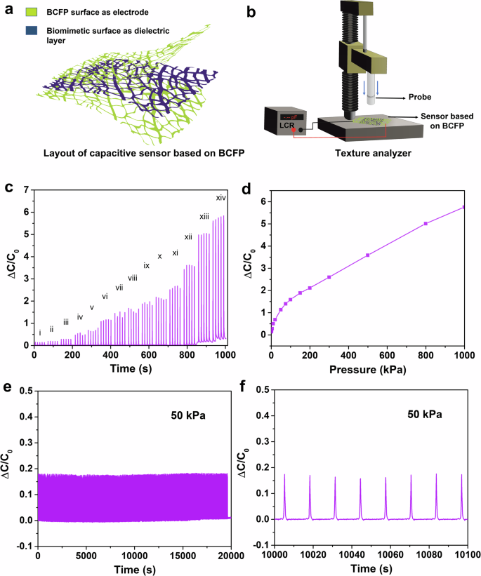
a Representation image of the BCFP based capacitive pressure sensor. b Pressure sensor characterization using the texture analyzer and LCR meter. c the change in relative capacitance with variation in pressure, (here, pressure ranges are i = 1 kPa, ii = 2 kPa, iii = 5 kPa, iv = 10 kPa, v = 20 kPa, vi = 50 kPa, vii = 75 kPa, viii = 100 kPa, ix = 150 kPa, x = 200 kPa, xi = 300 kPa, xii = 500 kPa, xiii = 800 kPa, xiv = 1 MPa). d represents the change in relative capacitance as a function of pressure. e shows the stability in the signal response of the capacitive pressure sensor when dynamically loaded with a pressure of 50 kPa for 1500 cycles. f magnified image of e, showing stability in relative capacitance response.
To demonstrate the BCFP’s application in real-life conditions, the pressure sensor made from BCFP was directly mounted onto the fingertip of a robotic hand using encapsulation tape. This allowed the robotic hand to possess a sensation of touch due to the presence of the pressure sensor. The tactile sensor exhibited changes in relative capacitance, indicating when a touch was sensed. Figure 7a depicts the change in relative capacitance of the sensor with each touch realized on the robotic finger. Additionally, this technology can be used in prosthetic limb movement detection, human motion detection, etc.
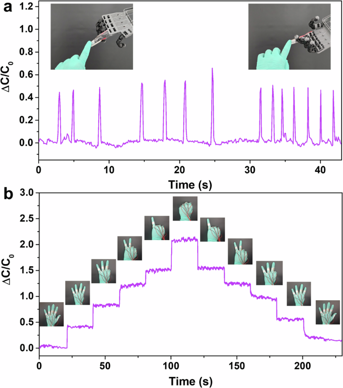
a Demonstration of BCFP based touch sensor on robotic hand and detection of touch sensation by observing the change in relative capacitance signal. b Demonstration of a multi-functional smart sensing glove that integrates pressure sensors using the BCFP electrodes for finger gesture detection.
We have also demonstrated the application of the capacitive sensor in real-time monitoring of human activities, taking advantage of its stable response and cyclic stability under various applied pressures. To monitor different finger gestures, a smart wearable nitrile glove was fabricated using capacitive sensors. The fabrication process involved mounting the BCFP-based capacitive sensors on each finger of the glove. The idea is to move the fingers after wearing the gloves, creating a pressure change on the sensor, which responds with a relative capacitance change depending on the pressure sensed. The total capacitance of these sensors was maintained for gesture monitoring by connecting them in parallel. The total capacitance of the smart glove is calculated using the following Eq. (1) 44:
A series of finger gestures were performed, with each gesture held for ~20 s. As shown in Fig. 7b, the smart glove successfully identified finger movements, showing consistent and reproducible capacitance changes in response to the pressure generated by individual gestures. Additionally, the capacitive sensor affixed to the wrist exhibited consistent patterns of change in relative capacitance in real-time response to wrist movements. During these demonstrations, no layer delamination or device failure was observed, highlighting the durability of the devices in practical applications.
To demonstrate BCFP’s applicability in other applications, we used BCFP as transparent heater and tested its performance. The Joule heating characteristics were evaluated by applying small continuous DC voltages between the two edges of the surface, and the resulting infrared (IR) images were recorded to observe the heat distribution (Supplementary Fig. 11). The BCFP surface exhibited uniform heating across its structure, demonstrating its potential for applications requiring efficient and even thermal management. Hence, BCFP surfaces can be used in energy and healthcare applications, particularly in transparent and stretchable heaters, without compromising other functional properties like breathability or stretchability.
The results indicate that conductive surfaces based on biomimetic fractal patterns have the potential to serve as breathable, stretchable, and transparent conductive surfaces for flexible electronic devices. Additionally, these surfaces are mechanically stable. It is noteworthy that the stretchability and transparency of the surfaces can be enhanced by using unique fractal architectures, which offer greater transparency and stretchability. The method proposed in this study is versatile, allowing for increased transparency and stretchability by using various types of polymers that are intrinsically more stretchable and transparent. Nevertheless, the leaf skeletons used in this study are not the only natural materials that can serve as inspiration. Many unexplored biological surfaces—such as skeletons of other leaves and plant-based membranes—may offer interesting, interconnected architectures at the microscale, good stretchability, strong adhesion to conducting nanomaterials, and maintain optical transparency and breathability.
Regarding sustainability, the process uses less energy, and these microstructures are created outside of cleanrooms. The biomimetic procedure can also be performed using sustainable polymers. For precise and large-scale production, CAD models can be created based on the biotic designs and their corresponding FEM models, allowing for the mass production of these biotic designs with master collectors. Furthermore, AgNWs can be replaced with more sustainable or functional nanowires or other conducting materials, depending on the device’s requirements.
Discussion
In conclusion, we successfully developed a new method for the biomimetic microfabrication of leaf skeleton-based fractal surfaces using modified electrospinning. The resulting freestanding biomimetic microfractals exhibited ~90% replication accuracy, high transparency, stretchability, and breathability. We demonstrated the versatility of this method by using various polymers and immobilizing AgNWs to create BCFP with high conductivity and transparency. The BCFP conformally attaches to the skin and functions effectively as e-skin and tactile pressure sensors. The BCFP’s good performance, including transparency, flexibility, moisture resistance, and ability to allow perspiration evaporation, highlights its potential for long-term use in epidermal sensors and advanced bionic skin applications. This study paves the way for scalable and integrable biomimetic microfabrication techniques in flexible electronics.
Methods
Materials
To prepare the flexible substrate via electrospinning, Nylon-6 (N-6), Polyvinyl Alcohol (PVA), Polyurethane (PU) and Polycaprolactone (PCL) were purchased from Sigma Aldrich. Silver nanowires (AgNW) having dimension 70 nm × 40 µm (W × L) were also purchased from Sigma Aldrich for the fabrication of stretchable BCFP. Cellulose tape for the fabrication of the capacitive sensor and copper tape for the heater fabrication were purchased from 3 M. An acidic plating solution consisting of 1 M H2SO4 (95-97% H2SO4, 1.00731.1011 Merck Emsure, Merck), 0.5 M CuSO4 (CuSO4·5H2O, 209198-500G copper (II) sulfate pentahydrate, ACS reagent, ≥98.0%, Sigma-Aldrich), 1 μM HCl (37% HCl, H 396 Romil-SpA Super Purity Acid, Romil), and ultrapure deionized H2O (18.2 MΩ cm, Merck Milli-Q) were purchased.
Fabrication of biotic collectors
To fabricate biotic collectors for the novel electrospinning method, different leaf skeletons have been utilized. The leaf skeletons were purchased from “Leaf Vein Crafts”, Toronto, Canada. Different leaves have been used due to variations in their microstructure dimensions and porous features, which directly affect properties like stretchability and transparency7,12. The fabrication process involves two steps: In the first step, the leaf skeletons are cut to the appropriate dimensions and then dried after being cleaned with DI water. Next, using physical vapor deposition, the leaf skeleton surfaces are sputtered with a thin layer of Au until a thickness of ∼30 nm is achieved on both sides. This ensures sufficient conductivity through the leaf skeleton surface for electrodeposition28,39. In the second step, Cu is deposited on the surface of the Au-coated leaf skeletons using the electrodeposition method. The electrodeposition was made in a 1 L polypropylene beaker using a power source (Thurlby Thandar TSX3510 DC Power Supply). At room temperature, electrodeposition was conducted using galvanostatic method where an Au-coated leaf skeleton served as the cathode and a copper foil (99.99%) served as the anode. A stand was used to support the electrodes used in the experiment and the electrodes were connected to the power supply using Cu alligator clips. To achieve the necessary mechanical strength for using the leaf skeleton as a collector in the electrospinning setup, a thick Cu coating was required. The electrodeposition was conducted for ~45 min which corresponds to a thickness of 10 μm cm–2 Cu film on an even surface28,39. This coating method ensured high reproducibility of the same Cu coatings on multiple leaf skeletons having different feature sizes and porous areas. After electrodeposition, the samples were cleaned with DI water and dried with an air blower. For simplicity, the surface area of a leaf skeleton was approximated to be the same as that of an intact leaf. However, it should be noted that the actual surface area of a leaf skeleton and the thickness of the Cu film are different.
Biomimetic nanofabrication and instrument setup
A customized electrospinning setup was utilized to fabricate biomimetic surfaces. A schematic of the setup is shown in Fig. 1a. We modified an existing electrospinning setup (Spinbox® by Bioinicia, Spain) by removing the collectors. The metalized leaf fabricated in the previous section was used directly as the negative collector as the sheet resistance was <0.01 Ω sq–1. Due to the microfractal structure of the leaf skeleton, the nanofibers were directly collected on the surface, replicating the same pattern. Then, a 3D-printed PLA frame, attached with double-sided tape, was used to peel the replicated surface from the biotic collector.
For electrospinning, a 10 mL syringe was consistently used across all experiments. Four different polymers— N-6, PVA, PU, and PCL —were employed to replicate the leaf pattern to demonstrate that the leaf collector is effective with various types of polymers. Thus, depending on specific requirements, more stretchable or transparent polymers can be replicated using this new fabrication technique by simply adjusting the polymer choice. For electrospinning N-6 nanofibers, N-6 pellets were dissolved in formic acid at a weight ratio of 22%, and the solution was sonicated for 1 h at room temperature. A flow rate of 1 μL min–1 and a positive potential of 17 kV were applied were used after optimization procedures. For electrospinning of PVA nanofibers, a 15% weight ratio PVA solution was prepared using DI water as the solvent. The solution was sonicated for 30 min at room temperature before use. A positive voltage of 22.4 kV and a flow rate of 5 μL min–1 were used. For electrospinning PU nanofibers, a PU solution with a 5% weight ratio was prepared using a solvent mixture of DMF and DCM in a 1:1 ratio. The solution was stirred magnetically for 24 h at room temperature. A positive voltage of 21 kV and a flow rate of 8 μL min–1 were applied. For electrospinning PCL nanofibers, a 12% weight ratio PCL solution was prepared using DCM as the solvent through a bath sonication process for 1 h. A positive voltage of 25 kV and a flow rate of 10 μL min–1 were used.
Fabrication of conductive surfaces and tactile pressure sensors
To fabricate BCFP, AgNW with a concentration of 200 µg mL–1 was spray-coated onto the biomimetic surface mounted on a 3D printed frame. The collector was then exposed to a hot air gun from the front to remove and merge excess, low-concentration fibers interspersed among the microstructures of the leaves. This process makes the surface more breathable, as fibers remain only on the leaf structures. The AgNW firmly attaches to the surface due to the combined effect of heat and airflow. After the substrate cooled to room temperature, its conductivity was verified by measuring the surface resistance with a digital multimeter.
To test the BCFP, a 3 × 3 cm² PLA frame with double-sided tape was used to peel off the conductive surface from the biotic collector. To fabricate a capacitive sensor, these conductive surfaces were utilized along with a non-conductive replicated surface as the dielectric layer. Copper tape and copper wires were used at both ends of the device as electrical contacts. The fabricated bioinspired flexible sensor has dimensions of 3 × 1.5 cm².
Characterization
High-resolution surface analysis of BCFP was performed using an Apreo S field-emission SEM (Thermo Scientific Inc., Eindhoven, The Netherlands) at 2 kV with an operating current of 25 pA. Elemental analysis was conducted using an EDS attachment linked to SEM (Oxford Instruments UltimMax 100 EDS). All contact angle measurements were performed using an Attension Theta Optical Tensiometer (Biolin Scientific, Sweden) with the sessile drop method. Stress-strain data of substrates were recorded using a texture analyzer (TA.XT.plus100C, Stable Micro System). The strain measurement probe of the texture analyzer was calibrated to 1.5 cm, resulting in an active surface area of 1.5 cm × 1.2 cm experiencing tensile force during the measurements (Supplementary Fig. 12). The same texture analyser equipped with a cylindrical probe with a diameter of 10 mm was used to apply and vary the pressure on the capacitive pressure sensors. The relative change in capacitance of the capacitive pressure sensor was measured using the LCR meter (GW-INSTEK LCR-6300). A testing signal of 1 V at 1 kHz was employed for all measurements on the LCR meter. The sheet resistance of the TCEs was measured using the Ossila four-point probe system, which features a probe spacing of 1.27 mm.
FEM modelling
For FEM modeling, we employed ABAQUS, a commercial non-linear FEM software package, version 6.14, developed by Dassault Systems in France, to accurately simulate the mechanical loading responses of biotic architecture. The biotic designs were created as a CAD model in SOLIDWORKS® software, with the support of the optical camera images and SEM images of the leaf skeleton architectures. Once the CAD models are finalized, they are imported into the ABAQUS software. To ensure accuracy, the calibration option within ABAQUS is used to incorporate experimental stress-strain data, allowing for the precise assignment of mechanical properties. The intrinsic stress-strain properties of N-6 from the experimental results were utilized as input for the simulation run. The ABAQUS software is a highly dependable tool that offers exceptional precision when evaluating the mechanical properties of various materials.
To compare the experimental results with the theoretical predictions, FEM analysis has been conducted considering all biomimetic surfaces replicated with N-6, and the details are given in the materials and methods section. The SEM images of the L. lucidum, F. religiosa, and P. tremuloides skeletons are illustrated in Supplementary Fig. 13a, c, e. These images were utilized in the creation of sketches, which subsequently served as the basis for the CAD models shown in Supplementary Fig. 13b, d, f. To effectively simulate the mechanical behavior of the structure, a dynamic implicit quasi-static analysis is utilized. It is crucial to consider geometric nonlinearity, and this can be achieved by enabling the NLgeom (non-linear geometry) option in the step modulus.
The mesh refinement technique is conducted to obtain more reliable outcomes while minimizing computing time. Results show that decreasing the approximate global size to 0.16 mm leads to convergence of the strain-stress curve, so 0.16 mm is chosen for all simulation efforts. The replaced surface element type is a node quadratic tetrahedron of type C3D10.


Responses