Bottom-up fabrication of 2D Rydberg exciton arrays in cuprous oxide
Introduction
Achieving strong photon-photon interaction is a long-sought goal in quantum optics, holding the promise of transforming quantum information technologies. Photons emerge as compelling contenders for applications in quantum technology due to their resilience against environmental disruptions and capacity for long-distance transmission with minimal losses1,2,3,4. Nevertheless, the absence of photon-photon interaction in linear optical media presents a formidable challenge in constructing extensive optical quantum communication networks and scalable quantum devices2,5,6,7,8,9. For example, strong photon-photon interactions are indispensable to perform two-qubit gate operations in photonic quantum circuits10,11,12,13,14 and to execute quantum algorithms on a photonic chip using entangled photon pairs15. Interactions among photons can be obtained in nonlinear media such as Beta-barium borate16, Lithium Niobate17, and Potassium Niobate18. However, the χ(3) nonlinear susceptibility of these materials is typically very small (~10−20 m2V−2) to obtain interactions at a single- or few-photon level. Therefore, an alternative scheme is necessary to achieve substantial photon-photon interactions.
Recently, Rydberg atoms and atom arrays have emerged as promising candidates for manifesting significant optical nonlinearity19,20,21,22 at a few photon levels. Rydberg atoms are highly excited electronic states with a large principal quantum number (n), and they offer exotic properties like longer coherence time23,24,25 and extended wavefunction (scales as n2) giving rise to very strong, long-range dipolar and van der Waals (vdW) interactions scaling as n4 and n11, respectively26,27. Besides, Rydberg states are highly tunable via external electric and magnetic fields28 finding various applications in quantum computing and information29, quantum optics30,31,32, programmable quantum simulators33,34,35,36,37,38,39,40, precision classical and quantum sensing41,42,43,44 and metrology45. While substantial advancements have been achieved in Rydberg atom quantum technologies31,46,47,48,49,50,51, a solid-state Rydberg platform with Rydberg excitons could be very advantageous due to its lower technical complexity and inherent integration capabilities. Solid-state systems provide a robust and miniaturized alternative, with sample sizes typically in the micron range, enabling them to fit into very compact experimental setups. This facilitates the easy tuning and control of individual excitons and allows for straightforward, controllable scalability. Additionally, with their inherent nature as an open quantum system, such platforms will make a unique testbed for the study of non-equilibrium quantum many-body physics52,53,54.
So far, Rydberg excitons have been observed in a few materials, such as two-dimensional monolayer transition metal dichalcogenides55,56,57,58 and perovskites59,60,61. Among them, cuprous oxide (Cu2O) is the only semiconductor where Rydberg states up to n = 30, natural bulk crystals, have been observed at cryogenic temperatures62. Cuprous oxide is a direct bandgap semiconductor (Eg = 2.17 eV), and its electronic transitions from different valence bands to different conduction bands give rise to four distinct Rydberg exciton series (yellow, green, blue, and violet series) named after the color of photons they emit63. In the yellow series, both the conduction band and valence band have the same parity, resulting in dipole-allowed p-excitons along with long-lived quadrupole-allowed yellow 1s-orthoexciton state64,65, making it significantly distinct from other excitonic systems. Furthermore, the large binding energy of Cu2O (~98 meV) facilitates the observation of high-lying excitonic states without succumbing to thermal ionization66.
Although natural bulk Cu2O crystals can support Rydberg excitons, both in an unbounded crystal63,67,68,69 and within confined pillars70, impurities and oxygen/copper vacancies negatively affect the quality of these excitons71. Therefore, producing controlled, high-quality synthetic Cu2O films is desirable. This approach also allows precise control over film thickness, making it comparable to the Rydberg blockade radius, where only a single exciton is allowed, thus enabling extreme nonlinearity at the single-photon level. The Rydberg blockade radius can extend beyond several microns for higher-order excitonic states (see Supplementary Materials, Section 4, and Supplementary Fig. S4). Therefore, developing an appropriate growth method to precisely control the film thickness is essential for entering the blockade regime. Utilizing recently developed CMOS-compatible growth techniques72,73, we employed a thermal oxidation method for the bottom-up fabrication of 2D arrays of Cu2O. Through non-resonant photoluminescence (PL) spectroscopy, we demonstrated the robustness of the fabricated arrays as well as the reproducibility and consistency of the Rydberg excitonic levels across 3000 × 600 μm2-large chips. Combined with locally addressable techniques such as spatial confinement74, strain75, electric fields76, and hybridizations with photons in structured microcavities77,78,79, this bottom-up fabrication scheme establishes a foundation for realizing versatile programmable Rydberg exciton arrays, akin to Rydberg atom arrays, which pave the way for advancements in scalable, on-chip, and highly tunable quantum technologies. Moreover, the thermal oxidation method employed in this study effectively reduces vacancy concentrations (see Supplementary Fig. S5), establishing it as a reliable platform for on-chip quantum devices. This method holds significant potential for simulating many-body dynamics with Rydberg excitons in Cu2O, including applications such as solving the Maximum Independent Set (MIS) problem80, generating single photons through the Rydberg blockade mechanism81, creating Rydberg exciton-polaritons to explore strongly correlated phases of matter using light on a chip79, and facilitating the study of driven-dissipative systems with Rydberg exciton-polaritons82.
Results and Discussion
The fabrication was started with a 700 nm-thick Cu film patterned using photolithography, followed by a liftoff process. The Cu regions were oxidized at high temperature and low pressure to form Cu2O. In Fig. 1(a), microscope images depict circular and square Cu2O regions with nominal side lengths and diameters of 14 μm and 16 μm. The actual diameters and side lengths of the Cu2O array sites deviated from the nominal values of the Cu regions. The thermal oxidation of Cu resulted in a 30% increase in size (cf. Supplementary Figs. S1 and S2). Figure 1b presents SEM images illustrating the 2D terrace-like growth of Cu2O around the periphery of the circular and square regions. In some sites, isolated Cu2O single-crystalline micro-particles were observed at the center, which significantly contributed to the PL signal (cf. Supplementary Fig. S3 (a) of the Supplementary information). Furthermore, Fig. 1c shows the size distribution of Cu2O particles across all regions with varying dimensions, indicating an average size of ~2.8 μm with a standard deviation of ~0.8 μm.
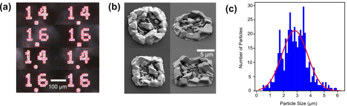
a Optical microscope images of circular and square Cu2O regions (the dots of the decimal numbers) with nominal radii and side lengths of 14 and 16 μm, respectively. The Cu2O regions showed Ruby color like natural gemstones. b SEM images of the same Cu2O regions demonstrated the two-dimensional growth of crystalline, terrace-like micro-particles. c Size distribution of 500 Cu2O micro-particles in various array sites showed a normal distribution with a mean size around 2.8 μm.
The low-temperature non-resonant PL spectrum from the yellow Rydberg exciton np series (570–580 nm) and phonon-assisted transitions (({Gamma }_{3}^{-}) and ({Gamma }_{4}^{-})) along with yellow 1s orthoexciton (600–625 nm) are shown in Fig. 2 for Cu2O arrays. The vermilion curve represents the average PL spectrum of Cu2O arrays across all regions with varying nominal side lengths, whereas the shaded region delimits the measurements’ statistical distribution. We noted that the PL signals in the Cu2O array were remarkably stable, exhibiting minimal spectral diffusion and blinking effects. Moreover, the sample showed no evidence of degradation after repeated temperature cycling or under high laser power excitation.
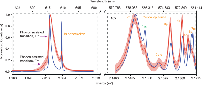
The left-hand side of the figure (600 – 625 nm) illustrates ({Gamma }_{3}^{-}) and ({Gamma }_{4}^{-}) phonon-assisted transitions, along with the yellow 1s-orthoexciton transition, whereas the right-hand side (570–580 nm) displays the photoluminescence (PL) from the yellow np Rydberg exciton series. The ({Gamma }_{3}^{-}) phonon-assisted transition in the thin-film sample exhibits a narrower linewidth and a more pronounced 1s-orthoexciton transition compared to the arrays, where the 1s-orthoexciton transition is relatively broader and weaker in intensity. In the yellow exciton series, exciton peaks up to n = 5p (7p) were observed for arrays (thin-film) in the PL spectrum. The 1s transition of the green series (denoted as 1sg) and 3s-d transitions are also discernible in the PL of the yellow exciton series. The yellow exciton spectrum is magnified by one order of magnitude to adequately display it alongside phonon replicas. The vermilion-shaded region indicates the area of statistical uncertainty across all measurements.
For comparison, the PL spectrum of a 700 nm Cu2O film fabricated using the thermal oxidation method under the same conditions is also shown with a solid blue line. Due to the lower count of yellow excitons compared to phonon-assisted transitions and yellow 1s orthoexciton, these counts were multiplied by 10 to be visible on the same scale. In the site-selective Cu2O arrays, exciton peaks up to 5p or 6p in the yellow series were visible for all array sizes examined in the experiments. As the energies of higher-order excitons approach the bandgap energy of Cu2O (Eg = 2.17 eV), and the oscillator strengths diminish with increasing the principal quantum number (n), the spectral lines overlap, complicating the resolution of individual peaks. The large linewidths of the p-excitons arose from exciton-phonon scattering originating from lattice vibrations and imperfections83. The heterogeneity of the sample led to variations in the PL spectra across the sample. Additionally, the positions and line widths of exciton peaks exhibited slight variations between particles within the same array and among different arrays (see Supplementary Figs. S6 and S7).
As can be seen, the exciton peaks (2p − 5p) of the array sample were redshifted compared to the thin-film sample. Besides, the ({Gamma }_{3}^{-}) phonon-assisted transition in the thin-film sample demonstrated a narrower linewidth compared to the array sample, yielding a lower effective exciton temperature. The energy shift was much larger for the 2p peak because of stronger screening of Coulomb interactions in these states and hence larger quantum defect δ(n, T)65. In Fig. 2, the first additional peak between 2p and 3p exciton transitions was attributed to the 1s peak of the green exciton series63,84. Additionally, the even-parity 3s − d transition was observed in the yellow exciton series spectrum, arising from the mixing of the L = 0 (s orbital) and L = 2 (d orbital) states85. Such even-parity transitions have also been detected in the PL studies of bulk natural crystals through cyclotron resonance two-photon excitation86. Beyond their presence in bulk crystals, the 1sg and 3s − d peaks were also observed in PL measurements of synthetic thin films of Cu2O72. The difference in the transition strength can be attributed to the reduced crystallinity in the thin films compared to bulk crystals.
For a quantitative study of the Rydberg excitons in the array, we used a symmetric Lorentz lineshape to fit αn(E) associated with the nth exciton transition65,66,
where En is the energy of the nth transition, Γn is the corresponding linewidth, and fn is a scaling factor that is proportional to the oscillator strength.
In Fig. 2, in addition to the Rydberg series, the PL also encompassed a distinctly sharp yellow 1s-orthoexciton peak (approximately at 610 nm) alongside the ({Gamma }_{3}^{-}) and ({Gamma }_{4}^{-}) phonon-assisted relaxations of the 1s state characterized by a Boltzmann-tailed profile. We conducted a fitting procedure for the yellow 1s-orthoexciton peak, from which we derived both its energy and linewidth. The Boltzmann-like phonon-assisted transitions (({Gamma }_{3}^{-}) and ({Gamma }_{4}^{-})) were convoluted with a Gaussian function to account for the spectrometer’s instrumental response. Subsequently, the effective temperature (Teff) of the excitons was derived from the resultant fit parameters (cf. Supplementary Section 2 and Supplementary Fig. S3b). The data depicted in Fig. 2 reveals that a broader linewidth of the phonon-assisted transition (({Gamma }_{3}^{-})) in arrays corresponded to a higher effective exciton temperature. Consequently, the phonon-assisted transition predominated over the yellow 1s orthoexciton, leading to decreased counts in the 1s state. This observation was drawn by comparing the vermilion and blue curves, which corresponded to the array and thin-film samples, respectively. Furthermore, in the thin-film sample, the resolution extended up to 7p peaks within the yellow exciton series.
Figure 3a and b show the variations in both energy and linewidth of the yellow 1s-orthoexciton transition across the array sample, respectively. Since the PL resolution (3.3 μm spot size on the sample) is comparable to the size of the Cu2O microparticles, as shown in Fig. 1c, the PL was effectively collected from these microparticles (the crystallite constituents within each array), regardless of the overall size of the arrays. Due to the inhomogeneity of the film, the PL exhibits spatial variation across individual disks. Therefore, each data point in Fig. 3a and b represents the averaged exciton energy derived from a fitting procedure performed on a set of 12 identical array sites with the same dimensions. The associated error bars signify the standard deviation across this ensemble. The energy and linewidth of the 1s-orthoexciton in a thin-film sample were illustrated by a horizontal black dashed line in both plots.
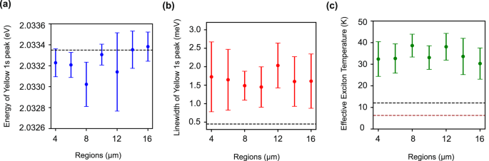
a Energy of 1s-orthoexciton (statistical average over many arrays having the same size) from regions of all sizes. Here, for all regions, the energies of yellow 1s-orthoexciton peaks in arrays showed a redshift compared to the thin-film sample (black dashed line). b Linewidth (FWHM) of yellow 1s-orthoexciton from all Cu2O arrays. The 1s-orthoexciton peak from the thin-film sample (black dashed line) demonstrated a narrower linewidth than arrays. c The effective temperature of excitons from all regions extracted by fitting the phonon-assisted transition using a Maxwell-Boltzmann distribution function convoluted with a Gaussian. The black dashed line depicts the effective exciton temperature for the thin-film sample, whereas the brown dashed line is the temperature of the cryostat sample stage. The effective temperature of the excitons was different from the sample stage temperature, which was fixed at 6.3 K. On the other hand, for thin-film samples, the effective exciton temperature was much smaller, around 12.07 K. The sample temperature was different from the cryo stage temperature because of the poor thermal conductivity of the quartz substrate. The higher effective exciton temperatures for arrays contributed to the linewidth broadening and redshift of the 1s-orthoexciton peak. Error bars are statistical error bars for all figures.
While Fig. 3(a) illustrates a redshift in the 1s-orthoexciton energies in Cu2O arrays compared to the thin film, panel (b) shows that the linewidths of excitons in arrays are broader than those in the thin-film sample. Finally, in Fig. 3c, the effective exciton temperature of the array sample was plotted alongside that of the thin-film sample (black dashed line) and the cryostation cold finger temperature (brown dashed line). For the thin-film sample, the effective exciton temperature of ~12 K was closer to the platform, i.e., 6.3 K, with slight deviations attributed to the limited thermal conductivity between the cold finger and the sample due to the quartz substrate’s poor thermal conductivity. Across all array sites, however, the effective exciton temperatures exceed the cryostation’s platform temperature by 20 K to 40 K. Besides the aforementioned reasons for the discrepancy between the sample’s and the cold finger’s temperature, the higher exciton temperature in the array sample compared to the thin film can be attributed to the reduced thermal contact of the isolated Cu2O islands with the substrate, leading to insufficient cooling. This local heating led to a spectral redshift of the resonant energies and the linewidth broadening in arrays compared to thin-film samples, as depicted in Fig. 3a and b, respectively. Moreover, the inhomogeneous broadening of the spectral lines may also result from sample inhomogeneity, leading to imprecise alignment of the spectral lines in energy. In addition to increased exciton temperature, this is another potential factor contributing to linewidth broadening. It is worth mentioning that the modification of the energies, linewidth, and effective temperature revealed the uniformity among array sites despite the large sample size, confirming the robustness and overall consistency of the exciton properties.
To investigate the spatial heterogeneity of the Rydberg exciton properties across the sample, we presented the energies and full width at half maximum (FWHM) linewidths of the yellow exciton series of the array sample in Fig. 4a and b, respectively. The thin-film data are represented by the black dashed line in each panel. While the energies and linewidths of Rydberg excitons showed a generally similar trend across different sites and arrays, the remaining discrepancies were attributed to variations in effective exciton temperature across the sample. The enhanced uncertainties in the linewidth of the 5p state primarily resulted from fitting inaccuracies. Given the proximity of the 5p state energy to the bandgap energy of Cu2O (Eg = 2.17 eV) and potential overlap with other peaks, accurately determining the linewidth was challenging. Similar to the energy of the yellow 1s orthoexciton, the energies of the np excitons in the Cu2O array showed a systematic spectral redshift compared to the thin film due to local heating.
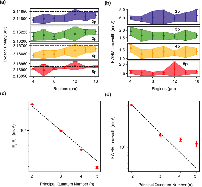
a The variation in the energies of 2p, 3p, 4p, and 5p excitons was examined across arrays of different dimensions. The dashed line represents the exciton energies observed in a thin-film sample. In all instances, the exciton energies within the arrays exhibited a red shift relative to the thin-film sample. b FWHM linewidths of the 2p, 3p, 4p, and 5p excitons and their variation for all arrays of different sizes. c Rydberg exciton energies as a function of n averaged over all regions with different nominal sidelengths from 4 μm to 16 μm. The black dashed line shows the n−2 trend of the hydrogenic energy levels from bulk natural Cu2O sample. The 2p, 3p, and 4p exciton energy followed the trendline, whereas the 5p exciton significantly deviated from it. d FWHM of yellow exciton series a function of principal quantum number (n). The black dashed line shows the n−3 trend. For 4p and 5p exciton, their linewidths significantly deviated from the trendline and reached a plateau for higher principal quantum numbers. Error bars are statistical error bars for all figures.
Finally, the dependence of Rydberg exciton energy and linewidths on the principal quantum number (n) is illustrated in Fig. 4c and d, respectively, obtained from the averaged data across all Cu2O arrays. In Fig. 4c, the dashed black line shows the anticipated hydrogen-like energy scaling of n−2 with the principal quantum number n. As can be seen, the observed exciton energies exhibited slight deviations from this power-law scaling. The notable difference in the 2p energy primarily arose from quantum defects attributable to the intensified Coulomb interaction with valence band holes. The deviations for higher states, e.g., 5p, on the other hand, can arise due to the higher susceptibility of these states to the size and the non-spherical symmetry of the electron-hole potential. As a result, the energy of excitons exhibited deviations from the ideal hydrogenic series. In Fig. 4d, the linewidths of yellow excitons were plotted vs. the principal quantum number n. The linewidths of the excitons can be modeled as66
where Γn is the FWHM linewidth of the nth state and α is a parameter capturing the power-law scaling of the p-Rydberg states. For large n, this asymptotically approached the well-known scaling of n−3 for s-type hydrogenic Rydberg states (black dashed trendline in panel (d)). On the other hand, β is an empirical fitting parameter that models the observed plateau in several experiments66,87,88. As can be seen, the experimental linewidths reached a plateau following previous results66. Although several hypotheses have been proposed for this behavior, including collisions with free electron plasma, dense clouds of ground-state excitons, or phonons, delineating the root cause requires a separate study in a sample where more Rydberg lines are attainable.
In this study, we operate in the low exciton density regime, approximately 1017 m−3, where exciton-exciton interactions can be neglected. To enter the blockade regime, the exciton density would need to be on the order of 1022 m−3 (as detailed in Supplementary Materials, Section 3). For instance, to observe blockade effects for 5p excitons, the thin-film thickness should be around 179 nm, with an interaction strength on the order of GHz. However, in our study, the sample thickness is approximately 700 nm, meaning we are not operating in the blockade regime for 5p excitons. To observe blockade over a distance of 2 microns, an n = 14p Rydberg excitonic state would be required.
Conclusions
In this study, we have demonstrated a CMOS-compatible bottom-up growth and fabrication of 2D cuprous oxide arrays on a transparent substrate and observed Rydberg exciton states up to 5p through non-resonant photoluminescence spectroscopy at cryogenic temperatures. While several other strategies for growing synthetic Cu2O thin films exist, such as the optical floating zone method89, the growth from melt90, reactive sputtering91,92, metal-organic chemical vapor deposition (MOCVD)93 and electrochemical deposition94,95, our robust fabrication method provides the monolithic site-selective growth of Cu2O islands and array sites without noticeable degradation of the optical properties over time and after several cooling-heating cycles. We studied the spatial variations of the photoluminescence spectrum of Rydberg excitons and ensured the reproducibility of the results and robustness of the excitonic features across a large area of 3000 × 600 μm2.
This study opens up new avenues for creating arbitrary arrays of Rydberg excitons akin to Rydberg atom arrays. When combined with several established local addressability and fine-tuning schemes in solid-state platforms—such as laser power, AC/DC Stark shift, and surface acoustic waves—this platform offers a unique opportunity to study the non-equilibrium dynamics of lattice models with strong long-range interactions mediated by Rydberg excitons. The in-situ controllability of the array sites enables the dynamic mapping of optimization problems on an on-chip, programmable platform with favorable SWaP (size, weight, and power) features80. Moreover, the developed site-controlled grown Cu2O can be integrated with nanophotonic circuitry and plasmonic nanostructures to mediate strong interactions between photons via Rydberg excitons and control the optical properties of these unique states using the advanced toolbox of nanophotonics96,97.
Methods
Sample Preparation
A 10 mm × 10 mm chip was cut from a 4-inch quartz wafer and cleaned via Toluene, Acetone, and IPA (Isopropyl Alcohol) baths, each lasting 5 minutes in a sonicator. Subsequently, the chip underwent drying using a nitrogen gun to eliminate any remaining solvents. A consistent layer of photoresist (AZ1518), approximately 4 μm in thickness, was applied to the chip via spin-coating, followed by a baking procedure. A photolithography design incorporating circular and square shapes, ranging in nominal size from 2 μm to 16 μm for each shape, was implemented. The photoresist was developed using the MF-26 photoresist developer for 60 seconds, followed by a rinse with distilled (DI) water.
Following the photolithography process, a 5 nm titanium (Ti) adhesion layer was deposited via an e-beam evaporation, which was succeeded by 700 nm of copper (Cu). After deposition, the photoresist layer was removed. Examination via scanning electron microscopy (SEM) of the copper sample revealed the presence of peripheral “wings” on both circular and square copper islands (Supplementary Fig. S1a), attributed to excessive copper accumulation on the angled sidewalls of the photoresist after liftoff. These wings were observed to diminish upon oxidation of the copper islands at elevated temperatures, forming Cu2O. The chip underwent oxidation within a CVD furnace for an extended duration to ensure thorough oxidation, as referenced in previous studies72,73. Following oxidation, all copper islands turned into cuprous oxide, evident from optical microscopy images and scanning electron microscope (SEM) images as illustrated in Fig. 1(a) and (b), respectively.
Photolumiscence Measurement
A 532 nm CW laser was employed to assess the photoluminescence of the Cu2O arrays at 6.3 K. This methodology facilitated an examination of the characteristics of both the yellow 1s orthoexcitons and the yellow np excitons via PL investigations. The measurements were conducted under a constant power of 50 μW with a laser spot size around 3.3 μm (FWHM), with power stability maintained within 0.5% using an acoustic optic modulator (AOM) configured in a double pass setup, as outlined in our previous work73.


Responses