Coexistence and interplay of pseudomagnetism and flexoelectricity in few-layer rippled graphene

Introduction
Mechanical strain, similar to other approaches such as elemental or charge doping, stacking sequence, external field, and twisting, has become a powerful strategy in exploring novel quantum states of graphene and other two-dimensional (2D) systems1,2,3,4,5,6. However, for graphene, an isotropic or uniform strain is difficult to induce significant variations in the band structure7,8. In contrast, a non-uniform strain can give rise to pseudomagnetic field (PMF), which can reshape the band structure near the Fermi surface and lead to pseudo-Landau-level sequences9,10. Such strain-induced pseudomagnetism with opposite signs in the two valleys of graphene, which does not break time-reversal symmetry, displays similar physical behavior to graphene under a real external magnetic field that breaks the time-reversal symmetry. This type of non-uniform strain can naturally reside in rippled graphene that is fabricated during thermal cycling on uneven-growth substrates. Indeed, strain-induced PMF effects in graphene have been experimentally and theoretically reported over the last decade11,12,13,14,15,16,17, and, benefitting from the latest advances in experimental techniques, have received increasing attention in more recent years. For example, graphene placed on black phosphorus generates a PMF with tunable spatial distribution and intensity18. Undergoing a thermally induced buckling transition, graphene on NbSe2 or hexagonal boron nitride (h-BN) substrates can create a periodic PMF that causes the emergence of flat bands, thereby providing a new platform for correlated electronics19. The PMFs have also been observed in twisted bilayer graphene, which can be simultaneously tuned by the twisting angle and heterostrain20. Moreover, by placing graphene on proper nanostructures to induce global inversion symmetry breaking, the PMFs can be drastically enhanced to 800 T21. Further explorations of emergent magnetic fields in twisted bilayer graphene have demonstrated anomalous or even quantized anomalous Hall effects upon proper electron filling22,23.
As another compelling property of 2D materials, flexoelectricity, describing a linear response of an electric polarization to strain gradients, can also be induced by non-uniform strain due to different growth conditions, the presence of defects, substrates, etc1,24,25. Given the atomic thickness of 2D materials, these systems can sustain large strain gradients through bending deformation, thereby exhibiting novel flexoelectric and flexomagnetic behaviors25,26,27,28,29,30,31. For instance, recent studies of bended graphene, such as nanoribbons, bubbles, and ripples32,33,34,35, have shown evidence of flexoelectricity in these systems. Besides graphene, 2D h-BN28,36, phosphorene37, germanium selenide (GeSe)38, transition metal dichalcogenides32,39,40 and van der Waals heterojunctions41 have also been shown to exhibit flexoelectricity upon mechanical bending. These extensive investigations have demonstrated that flexoelectricity in 2D materials has promising technological applications in future devices, including sensors, nanogenerators, micro-robots, optoelectronic, and flexible electronic devices.
In light of the fact that strain not only produces PMFs in graphene but also causes flexoelectricity, a natural and unexplored question arises: can the strain-induced behaviors of pseudomagnetism and flexoelectricity coexist or even interact favorably in the same 2D system such as graphene? The coexistence of magnetism and flexoelectricity can be manifested in the form of multiferroics, which may harbor exotic physical properties and offer new opportunities in multi-functional devices. Here we note that a highly related concept of electric polarization, ferroelectricity, has been demonstrated to coexist with magnetism in several 3D materials42,43,44,45, and more recently, the couplings of these two orders have also been theoretically investigated in a few 2D systems such as CrBr346, VOCl2 monolayer47, and chemically modified phosphorene48. Ferroelectrics are a class of materials with spontaneous polarization that can be switched by an electric field or external environment, whose polarization is typically determined by atomic structures, rather than by strain gradients as observed in flexoelectric polarization. Inspired by these developments, it is highly desirable to explore effective ways to empower graphene to simultaneously harbor pseudomagnetism and flexoelectricity under physically realistic conditions, thereby providing appealing platforms for realizing magnetoelectric multiferroic devices based on 2D materials.
Here, by using tight-binding (TB) models supplemented with selective crosschecks within first-principles theory, we present the first demonstration of the coexisting pseudomagnetism and flexoelectricity in both rippled graphene monolayer and bilayer and further establish the interplay of the strain-induced behaviors. First, we show that the non-uniform distribution of strain in a rippled graphene monolayer induces a synchronously modulated PMF that does not break the time-reversal symmetry. Nevertheless, the PMF breaks charge neutrality and gives rise to a spatially varying sublattice polarization, which results in the concomitant emergence of local in-plane polarization and global in-plane polarization in opposite directions. The range of the local polarization region can be reduced by half if the PMF exceeds a critical value, associated with a PMF-induced reversal of the electric polarization direction. Next, for a rippled bilayer, we show that the corrugated shapes of the top and bottom layers are synchronized as long as the ripple strength is below a critical value. For moderate ripple strengths, we observe substantially further enhanced pseudomagnetism in some regions of the bottom (top) layer and the disappearance of pseudomagnetism in the corresponding regions of the top (bottom) layer due to pronounced interlayer coupling, accompanied by simultaneous in-plane and out-of-plane polarizations with opposite directions. In addition, the flexoelectric patterns in both the monolayer and bilayer systems can be effectively modulated by the PMFs. The coexistence of pseudomagnetism and flexoelectricity in rippled graphene is not only of significant interest for fundamental understanding but also provides a new platform to explore phase-transition device applications.
Results
PMF in rippled graphene monolayer
As shown in Fig. 1, we focus on one-dimensional periodic graphene ripples without losing generality and assume that the period of the ripples is along the y (or armchair) direction and the translational symmetry is preserved along the x (or zigzag) direction. To consider experimentally achievable graphene ripples, we select the period of the ripple L as 106.5 nm ((L=500d,{d}=frac{3a}{2}), and a is the carbon-carbon bond length in pristine graphene), and the strength of the ripple (r=frac{h}{L}) (with h being the height of the ripple) within the range of (0(,0.10)). Such ripples in both scale and strength are comparable with existing theoretical and experimental studies11,12,15,16,18,19. The shape of the ripple (Hleft(yright)), the strain tensor ({u}_{{yy}}), the PMF ({B}_{s}), and the nearest-neighbor hopping parameter (t) for a rippled graphene monolayer (see Methods) are illustrated in Fig. 1b1, b2, c, and d, respectively. We find that the maximum of the strain tensor(,{u}_{{yy}}) is located at (y=0,,250d,,500d), where (Hleft(yright)) equals 0. However, the absolute value of the maximum of the PMF ({B}_{s}) is around (y=62.5d,187.5d,,312.5d,,437.5d), where (Hleft(yright)) is (+h/2) or (-h/2). Since the period of the PMF is half that of the (Hleft(yright)), we can focus on the ripple properties in the range of (0 ,<, y,<, 250d).

a Top view of the atomic structure of a rippled monolayer, with different primitive cells and hopping parameters indicated. b1, b2 Side views of the ripples with different ripple strengths (r) in the period of (L=500d=106.5{rm{nm}}). The arrows in b1, b2 represent the flexoelectric polarized directions. c Variations of strain tensor ({u}_{{rm{yy}}}) (black solid line) and pseudomagnetic field ({B}_{s}) (red dotted line) with the spatial location (y) for r = 0.10. d The corresponding hopping parameters ((t)) and relative hopping parameters between nearest-neighbor sublattices ((Delta t)) as the function of y. The gray dotted and black solid lines represent ({t}_{mathrm{1,2}}) and ({t}_{3}), respectively. The magenta dotted and red solid lines indicate (2Delta {t}_{mathrm{1,2}}=2left(left|{t}_{mathrm{1,2}}left(i+1right)right|-left|{t}_{mathrm{1,2}}left(iright)right|right)) and (Delta {t}_{3}=left|{t}_{3}left(i+1right)right|-left|{t}_{3}left(iright)right|)), respectively.
The band structures and density of states of the rippled monolayer are calculated within the TB model, with the highest-valence and lowest-conduction bands around one of the valleys and the local density of states (LDOS) at (y=62.5d) shown in Fig. 2a, b. Prominent changes in the bands and LDOS emerge when the strength of the ripple (r) increases. With a strong strength ((r=0.10)), the ripple exhibits the partially flat bands at zero energy, whereas for the ripple with a moderate strength ((r=0.05)), the system largely recovers its linear electron dispersion. In addition, with the increase of the ripple strength, the center of the flat bands dramatically shifts away from ({k}_{x}=frac{2pi }{3sqrt{3}a}), where the Dirac point of pristine graphene is located. Such shifts were also observed in related density functional theory (DFT) studies12. More intriguingly, these partially flat bands are created by the PMF due to the non-uniform strain in the rippled graphene, which is called the n = 0 pseudo-Landau level, the analog of the Landau level in a real magnetic field49,50. The effect of these flat bands is also reflected in the LDOS, indicating a strong charge imbalance between the A and B sublattices. Specifically, with a strong strength of the ripple (for example, (r=0.10) in Fig. 2b), the DOS has a peak at zero energy in the A sublattice but exhibits a gap in the B sublattice at (y=62.5d). In order to check the validity of our TB model, we have also carried out DFT calculations of the band structures for a ripple in a smaller size, and the results are consistent with the TB calculations (see Supplementary Note 1).
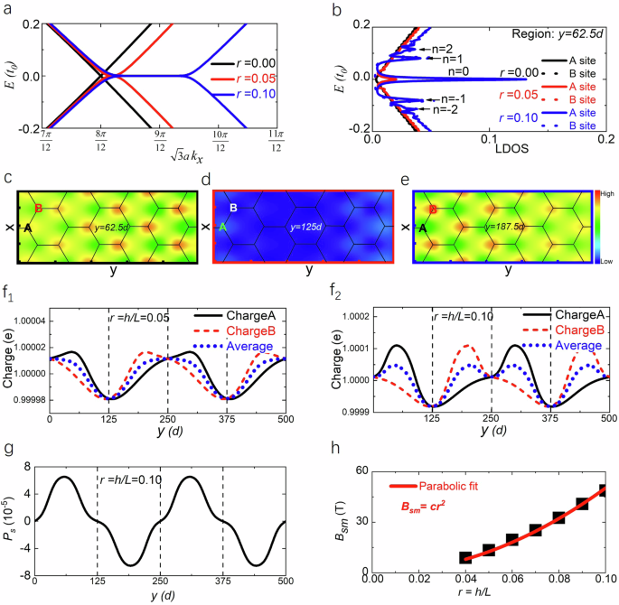
a Band structures of the rippled monolayers with different ripple strengths in the TB model. b The corresponding local densities of states (LDOS) at the location of (y=62{boldsymbol{.}}5d). c–e Charge densities in different regions indicated in Fig. 1b2: black dashed box (c), red dashed box (d), and blue dashed box (e). f1, f2 Spatial charge distributions for r = 0.05 (f1) and r = 0.10 (f2). g Variation of the sublattice polarization Ps. h Relation between the maximum of pseudomagnetic field ({B}_{{sm}}) and ripple strength (r=h/L).
The intensity of the strain-induced PMF in the rippled monolayer can be determined by the positions of the pseudo-Landau levels or peaks in the LDOS that follow the expression ({E}_{n}={E}_{D}+mathrm{sgn}left(nright){v}_{F}sqrt{2ehslash {B}_{s}left|nright|})13,16,19, where ({E}_{n}) and ({E}_{D}) are the positions of the nth pseudo-Landau level and Dirac point, respectively, ({v}_{F}=3left|{t}_{0}right|a/left(2hslash right)approx 8.7times {10}^{5},text{m}/text{s}) is the Fermi velocity of pristine graphene, (e) is the electron charge, and (hslash =h/2pi) is the reduced Planck constant. For the case of (y=62.5d) and (r=0.10), we can easily identify the positions of different pseudo-Landau levels from the LDOS in Fig. 2b. By a proper fitting (see Supplementary Note 2), the maximum value of the PMF is obtained as ({B}_{{sm}}approx 48.8,{rm{T}}), which is consistent with the value of 40.6 T derived from ({B}_{0}=2.8times {10}^{3}{a}_{0}q) (({a}_{0}=sqrt{3}a,{q}=2pi /L)) reported earlier12. Using this scheme, an approximately parabolic variation of the ({B}_{{sm}}) with the ripple strength (r) is determined within the range of (0.04le rle 0.10), as indicated in Fig. 2h. It is noted that the electronic structures of the rippled monolayer with (r ,<, 0.04) have no obvious difference from that of pristine graphene, indicating that the PMF cannot be induced when the ripple strain is weak enough. The underlying reason is that the observation of the Landau levels requires that the magnetic flux (Phi) satisfies the condition of (beta Phi,>, 1)11,15. Here the magnetic flux corresponds to the area of the ripple (Phi sim tfrac{{h}^{2}}{{La}}), and (r ,>, 0.03) meets the condition for the considered ripples to exhibit the PMFs.
Based on experimentally obtained PMFs from graphene grown on black phosphorus18, NbSe2, hexagonal boron nitride19, or other proper architected nanostructures21, we believe that our rippled graphene monolayer model can be experimentally achieved, and the PMF can be tuned by the scale (L) and strength (r) of the ripple.
Sublattice polarization in rippled monolayer
A hallmark of a PMF is the sublattice electric polarization, which is reflected by the charge contrast between the sublattices51 as ({P}_{s}=left({C}_{A}-{C}_{B}right)/left({C}_{A}+{C}_{B}right)). Here, ({C}_{i}) with (i={rm{A; or; B}}) measures the charge on the (i) sublattice in a primitive cell. The Ps distribution for the (r=0.10) ripple is shown in Fig. 2g. In the region around (y=125d) (see the red dashed box in Fig. 1b2), since there is no strain or PMF (see Fig. 1c), the charge is uniformly distributed on the A and B sublattices (Fig. 2d); correspondingly, ({P}_{s}=0). In contrast, around the region with the highest PMF ({B}_{{sm}}approx 48.8,{rm{T}}) ((y=187.5d), see the blue dashed box in Fig. 1b2), the charge is accumulated on the B sublattice (Fig. 2e), leading to the maximum of the ({P}_{s}) with ({P}_{{sm}}=-6.5times {10}^{-5}), while around the region with the opposite PMF ((y=62.5d), see the black dashed box in Fig. 1b2), the charge favors on the A sublattice (Fig. 2c), yielding ({P}_{{sm}}=6.5times {10}^{-5}). The charge reversal on the two sublattices can also be seen from the variations of the charge on the sublattices with the spatial location y, as shown in Fig. 2f1 and f2. Indeed, such a charge reversal is the manifestation that the PMF has opposite signs in the K and K’ valleys due to the presence of time reversal symmetry14. Moreover, the triangular structures of the buckled graphene systems observed in the atomic-resolution scanning tunneling microscope images explicitly reflect such sublattice polarizations14,19, further confirming the reliability of our results.
The sublattice polarization can be understood from the hopping kinetic energy in the TB model. Given the fact that the hopping parameters ({t}_{mathrm{1,2}}) and ({t}_{3}) vary with (y) in the form of a cosine function, the hopping parameter difference (Delta {t}_{{1,2}}=left|{t}_{{1,2}}left(i+1right)right|-left|{t}_{{1,2}}left(iright)right|) or (Delta {t}_{3}=left|{t}_{3}left(i+1right)right|-left|{t}_{3}left(iright)right|) between the nearest-neighbor lattices does not remain constant, as shown in Fig. 1d. In the region of (0 ,<, y,<, 125d), the absolute values of the hopping parameters on the (i+1) lattice, (left|{t}_{mathrm{1,2}}left(i+1right)right|) and (left|{t}_{3}left(i+1right)right|), are larger than that on the (i) lattice, respectively. For example, for the A and B sublattices in a primitive cell indicated by an elliptical area in Fig. 1a, (left|{t}_{3}left(i+1right)right|) on the B sublattice is larger than (left|{t}_{3}left(iright)right|) on the A sublattice, while (left|{t}_{1}left(i+1right)right|) and (left|{t}_{2}left(i+1right)right|) are equal. Accordingly, the charge accumulates less on the B sublattice due to its larger hopping kinetic energy, but relatively favors to accumulate on the A sublattice. When considering the neighboring primitive cell highlighted by a shadowed rectangle in Fig. 1a, (Delta {t}_{mathrm{1,2}}) is larger than zero. As shown in Fig. 1d, (Delta {t}_{3}) in the elliptical primitive cell is larger than (Delta {t}_{{1,2}}) in the rectangular primitive cell, for instance, more than twice as large at the center of the (0 ,<, y ,<, 125d) region. Therefore, for the B-A-B sublattices in the rectangular and elliptical cells, charge prefers to accumulate at the A site over B site. In contrast, the charge on the B site is more than that on the A site in (125d ,<, y ,<, 250d) because of the reversed (Delta {t}_{{1,2}}) and (Delta {t}_{3}) and the relationship (left|Delta {t}_{3}right| > left|Delta {t}_{{1,2}}right|). It is noted that when the difference between (left|Delta {t}_{3}right|) and (left|Delta {t}_{{1,2}}right|) disappears (i.e., (left|Delta {t}_{3}right|=left|Delta {t}_{{1,2}}right|)), the charge would be uniformly distributed on the A and B sublattices, and thereby the PMF would vanish (see Supplementary Note 3).
Reversal of flexoelectric polarization direction in rippled monolayer
To explore flexoelectric polarization in the rippled monolayer, we further analyze the spatial charge distributions. The average charge between the A and B sublattices is not constant, but periodically varies with the spatial location (y) (with the period of (y=250d)). First, for the case of (rle 0.05), the average charge decreases monotonously in (0,<, y ,<, 125d), while it increases monotonously in (125d,<, y ,<, 250d) (see, for example, Fig. 2f1). This behavior empowers the rippled graphene with an in-plane flexoelectric polarization, whose polarized directions are indicated by the cyan arrows in Fig. 1b1. The value of the polarization can be calculated from the equation ({P}=frac{sum {Delta q}_{i}d}{S}), where ({Delta q}_{i}) is the charge difference between the adjacent primitive cells, and (S) is the area of the region, yielding ({P}_{1}=7.9times {10}^{-17},text{C}/text{m}) for both the (0 ,<, y ,<, 125d) and (125d ,<, y ,<, 250d) regions at (r=0.05). Note that this polarization calculation method is valid for rippled graphene, since it is a finite isolated system in the out-of-plane direction and will not encounter the ambiguity of the electric polarization definition due to different choices of unit cell for infinite periodic systems52,53,54. It is also noted that in contrast to semiconducting or insulating bulk materials, which are prone to electric polarization, 2D metallic materials can also exhibit electric polarization as long as the charge distribution is not uniform. For example, graphene bilayers and their moiré superlattices show the characteristics of electric polarization55, and the metallic material WTe2 has been reported to exhibit electric polarization as well56,57,58. It is worthwhile to point out that this in-plane flexoelectricity is intrinsically caused by strain gradient, but not by the PMF; in general, the latter can be ignored for ripples with the relatively weak strengths.
Next, for strong ripple strengths ((r ,>, 0.05), see for example, (r=0.10) in Fig. 2f2), the average charge first increases up to the maximum and then descends rapidly in (0,<, y,<, 125d), while in (125d ,<, y,<, 250d), it exhibits a mirror-symmetry behavior with respect to (y=125d). These results signify that the local flexoelectric polarization in (0, < ,y ,< ,125{d}) or (125d, < ,y, < ,250d) for (rle 0.05) becomes two parts with opposite directions in nature with the increase of r. Such a reversal of flexoelectric polarization direction is attributable to the presence of the relatively strong PMFs. The domain walls of these two parts of flexoelectric polarization are located near the midpoints ((y=62.5d) and (y=187.5d)). The calculated polarizations are ({P}_{1}=5.2times {10}^{-16},text{C}/text{m}) for (62.5d ,<, y ,< ,125d) and ({P}_{2}=2.7times {10}^{-16},text{C}/text{m}) for (0 ,<, y ,<, 62.5d), while the symmetrical results are obtained in (125d,<, y ,<, 250d). Here we emphasize that, to our best knowledge, such PMF-induced reversal of flexoelectric polarized direction is identified for the first time.
Given the above analysis, the rippled graphene monolayers exhibit local flexoelectric polarization, no matter of the weak or strong ripple strengths. One distinct feature is that the range of the local flexoelectric polarization region will be reduced by half at a critical ripple strength, associated with the emergence of the PMF-induced reversal of flexoelectric polarization direction. To determine this critical value, we calculate the spatial charge distribution for (r=0.06) (see Supplementary Fig. 3d). The average charge does not exhibit a monotonous behavior, but possesses an extreme point in (0 ,<, y,<, 125{d}) or (125d,<, y ,<, 250d), indicating that the critical ripple strength is ({r}_{c}=0.05), with the corresponding ({B}_{{sm}}approx 13.4,{rm{T}}). Such a critical transition behavior has also been firmly validated in our DFT calculations (see Supplementary Note 1).
The phenomenon of flexoelectric polarization direction reversal predicted near the critical ripple strength ({r}_{c}=0.05) is analogous to the experimentally observed and theoretically confirmed transition from one ferrielectric state to another in the ferroelectric material CuInP2S659,60, which is caused by the enhanced flexoelectric effect.
As for whether the shrinkage of flexoelectric domain walls is a result of PMF, an experiment can be designed to verify this finding. Scanning electron microscopy can be used to observe the range of electrically polarized domain walls in graphene grown on a flexible substrate. By adjusting the ripple strength of the flexible substrate, if the width of domain walls is found to be reduced by half, it would provide strong evidence supporting the validity of these results.
To elucidate the underlying mechanism of the reversal of flexoelectric polarization direction at the critical ripple strength, we revisit the hopping kinetic energy, since charge occupation on the lattice is completely decided by the hopping kinetic terms in the TB Hamiltonian without the on-site potential terms. When the ripple strength is weak, the hopping parameters (({t}_{mathrm{1,2}}) and ({t}_{3}) that are almost the same) and average charge distribution vary synchronously in the form of a cosine-like function. This behavior naturally results in the local flexoelectric polarization in (0 ,<, y,<, 125d) or (125d,<, y,<, 250d); meanwhile, the in-plane polarized directions in the two regions are opposite. When the ripple strength increases, the difference between ({t}_{mathrm{1,2}}) and ({t}_{3}) increases due to the non-uniform strain. The charge distribution on one sublattice keeps the cosine-like form, while the charge on the other sublattice has an extreme value in (0,<, y,<, 125d) or (125d, < ,y ,< ,250d) (see Fig. 2f1 and f2). This feature leads to the sublattice polarization, with the maximal polarizations located at the centers of the original flexoelectric regions ((y=62.5d) and (y=187.5d)) (see Fig. 2g) where the PMF also reaches the maximum value. Given the charge conservation, the charge transfers from two terminals to the middle in each of the original flexoelectric regions; in other words, electrons tend to accumulate around the centers of the original flexoelectric regions, where the PMF-induced electron localization is more significant. Therefore, the original flexoelectric polarization is transformed to two small flexoelectric regions with opposite directions over the critical value (({r}_{c}=0.05), associated with ({B}_{{sm}}approx 13.4,{rm{T}})).
Asymmetry in sublattice polarization and interlayer polarization of rippled bilayer
To construct a reasonable rippled graphene bilayer model, especially for understanding how the top rippled layer is dictated by the bottom ripples that are usually determined by substrates, we first perform some DFT calculation tests (see Supplementary Note 4). We find that as long as the strength of the bottom ripple ({r}_{b}) is not strong (({r}_{b}le 0.05)), the top ripples will keep step with the bottom ones, accompanied by a slight increase of the interlayer distance compared with that of pristine AB-stacked graphene bilayer (({d}_{0}=3.25mathring{rm A})). When ({r}_{b}) increases, for example, ({r}_{b}=0.10), the bilayer system is most stable when the strength of the top layer ripple is ({r}_{t}=0.03) and the interlayer distance is decreased to (0.90{d}_{0}). Since ({r}_{t}=0.03) is too weak to exhibit explicit changes in the electronic band structures caused by the PMF (see above discussion for the rippled monolayer), here we only consider an AB-stacked rippled bilayer with (L=500d), ({r}_{b}={r}_{t}=0.05), and the interlayer distance of (1.05{d}_{0}) for the TB calculations, as shown in Fig. 3. Note that both the top and bottom rippled layers possess the PMFs in this model system.
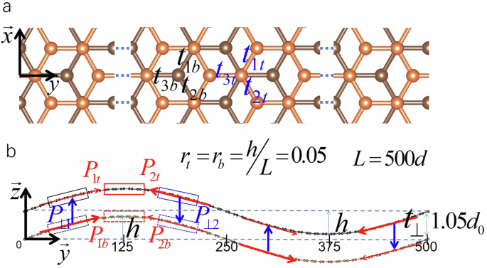
a Top view of the atomic structure of a rippled bilayer, with hopping parameters indicated. b Side view of the rippled bilayer with the top and bottom ripple strengths of ({r}_{t}={r}_{b}=0.05) in the period of (L=500d=106.5{rm{nm}}). The interlayer distance of 1.05d0 (d0 = 3.25 ({rm{mathring{rm A} }})) is the equilibrium distance obtained by the DFT calculations. The arrows in b represent the flexoelectric polarized directions.
The TB-based spatial charge distributions of the top and bottom layers are illustrated in Figs. 4a, b. Compared with the rippled monolayer (see Fig. 2f1), one distinct difference is that the charge distributions and corresponding average charge are all asymmetrical with respect to (y=125d) in the period of (0, (250d)). The other different feature is that the charge always favors on the same sublattice in the whole period, but the charge differences between the two sublattices vary significantly with the spatial location y due to the asymmetry of the charge distribution. For example, the charge on the top layer dramatically favors the B sublattices over the A sublattices in (125d ,<, y ,<, 250d), while it only slightly favors the B sublattices in (0 ,<, y ,<, 125d). Such features naturally lead to the asymmetry in the sublattice polarization, which is also clearly demonstrated by the charge density distributions shown in Fig. 4e–j.
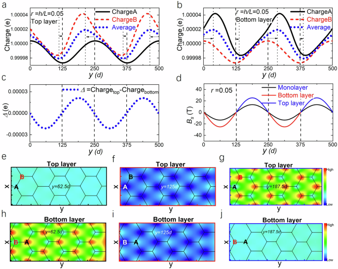
a, b Spatial charge distributions of the top (a) and bottom (b) layers. c Spatial distribution of the charge difference between the top and bottom layers. d Spatial distribution of the pseudomagnetic field ({B}_{{rm{s}}}). e–j Charge densities of the top (e–g) and bottom (h–j) layers in different regions indicated in Fig. 3b: black solid and dashed boxes (e, h) red solid and dashed boxes (f, i) and blue solid and dashed boxes (g, j).
To gain more insight into the sublattice polarization, we analyze the effects of the intralayer and interlayer hopping parameters in the TB models of both the pristine and rippled bilayers. Based on the TB model for a pristine AB-stacked graphene bilayer with ({t}_{mathrm{1,2}}={t}_{3}) (see Supplementary Note 5), we obtain that the charge distributes evenly on either sublattice but with a slight transfer between the A and B sublattices in each layer, and the two layers have the opposite charge distributions. The reason of charge difference between the sublattices in a given layer is that, for example in the bottom layer, the B sublattices have larger hopping energies than the A sublattices because the interlayer hopping ({t}_{perp }) is connected by B in the bottom layer and A in the top one (see Supplementary Fig. 7a). For the rippled bilayer, ({t}_{mathrm{1,2}}ne {t}_{3}) causes the variation of the sublattice polarization with the spatial location y for both layers. Due to the interlayer hopping ({t}_{perp ,j}), the charge distribution is further modified, thereby breaking the symmetry of the sublattice polarization within each period. Specifically, when ({t}_{perp ,j}) is very weak, the top and bottom layers largely preserve the charge distributions of the isolated rippled monolayers. With increasing the ({t}_{perp ,j}) (that connects one B sublattice in the bottom layer and A in the top layer; see Supplementary Note 6), the charge on B in the bottom layer significantly decreases, especially in ({125} ,<, {y} ,<, {250d}), where the charge initially favors the B sublattices. Meanwhile, the charge on the A sublattice increases, eventually leading to the charge dominance on A in the whole period after a critical value of ({t}_{perp ,j}). In particular, such charge variations on the B and A sublattices are not symmetrical with the spatial location, resulting in the asymmetry in the sublattice polarizations. The charge distribution and sublattice polarization in the top layer exhibit similar behaviors but with the exchange of the A and B sublattices.
Besides the sublattice polarization within each layer of the rippled bilayer, there also exists polarization between the two layers. As shown in Fig. 4c, the charge difference between the top and bottom layers varies with the spatial location y in the form of a cosine-like function, leading to the emergence of interlayer polarization. Specifically, the regions of (0 ,<, {y} ,<, 125d) and (125 ,<, {y} ,<, 250d) possess similar amplitudes of the polarizations but with opposite directions, and the polarization reaches the maximum ((pm 1.1times {10}^{-5})) in the middle of each region ((y=62.5d) and (187.5d)). At (y=0,,125d,,250d), the interlayer polarization is zero. Since the polarization depends on the spatial location, it can be attributed to the synergy of the interlayer hopping and intralayer PMFs. In contrast, for a pristine graphene bilayer, the interlayer-hopping-induced sublattice polarization (({P}_{{inter}}), given by (pm 7.6times {10}^{-6}) for the bottom and top layers, respectively; see Supplementary Note 5) does not depend on the spatial location.
Redistribution of the PMFs in rippled bilayer
In fact, the asymmetry in the sublattice polarization of the rippled bilayer with respect to the boundary of (y=125d) reflects the redistribution of the PMF in each layer compared with the case of the rippled monolayer. We first examine the region of (0 ,<, y ,<, 125d). For the top layer, the charge on the A sublattice is slightly less than that on the B sublattice ({left(right.C}_{A}^{t},<,{C}_{B}^{t}), see Fig. 4a); correspondingly, the maximum of the sublattice polarization ({P}_{{sm}}) decreases to (6.0times {10}^{-6}) from (9.1times {10}^{-6}) for the rippled monolayer. Since the LDOS does not have peaks, especially no 0th pseudo-Landau level (see Supplementary Note 7), the PMF disappears in this region. For the bottom layer, the charge significantly prefers to accumulate at the A over B sublattices ({left(right.C}_{A}^{b},gg, {C}_{B}^{b}), see Fig. 4b); thus, ({P}_{{sm}}) is dramatically enhanced to (1.6times {10}^{-4}). Not only that, compared with the rippled monolayer, the amplitude of the 0th pseudo-Landau level in the LDOS significantly strengthens (see Supplementary Note 7), implying that the PMF is enhanced in this region. Next, with similar analyses for (125d ,<, y ,<, 250d), we obtain that the PMF is enhanced in the top layer, whereas it disappears in the bottom layer. Given these results, the spatial dependences of the PMFs are displayed in Fig. 4d, where the relation of ({B}_{s}={B}_{{sm}}sin left(4pi y/Lright)) is adopted to estimate the PMF values because the Landau levels can hardly be explicitly observed in the regions with too low PMFs.
Coexistence and tunability of in-plane flexoelectricity and out-of-plane polarizations in rippled bilayer
As discussed in the rippled monolayer, the spatial charge distributions (see Fig. 4a, b) demonstrate that the local in-plane flexoelectric polarizations exist in each layer of the rippled bilayer. Since the strengths of the rippled bilayer (({r}_{b}={r}_{t}=0.05)) do not exceed the critical value ({r}_{c}=0.05) for the rippled monolayer, as expected, there is no reversal of flexoelectric polarized direction in (0 ,<, {y} ,<, 125{d}) or ({125}{d} ,<, {y} ,<, {250}{d}). However, due to the asymmetry of the sublattice polarization, the flexoelectric domain walls shift toward the left in the top layer and the right in the bottom layer by different distances (see Fig. 4a, b), compared with the monolayer case. For the top layer, the resulting flexoelectric region around ({0},<, {y} ,<, {125d}) enlarges, whereas the other flexoelectric region around (125d ,<, {y} ,<, 250d) shrinks; for the bottom layer, it is just the opposite. We further calculate the local in-plane flexoelectric polarization for the top layer to be ({P}_{1t}=8.7times {10}^{-17},text{C}/text{m}) and ({P}_{2t}=1.3times {10}^{-16},text{C}/text{m}) in (0 < y < 125d) and (125d ,<, {y} ,<, 250), respectively. The corresponding values for the bottom layer are ({P}_{1b}=1.3times {10}^{-16},text{C}/text{m}) and ({P}_{2b}=8.8times {10}^{-17},text{C}/text{m}). The directions of ({P}_{1t}) (({P}_{1b})) and ({P}_{2t}) (({P}_{2b})) are shown in Fig. 3b, indicating the local in-plane flexoelectric polarization in the rippled bilayer.
Besides the local in-plane flexoelectric polarization, the charge difference between the top and bottom layers (see Fig. 4c) and the corresponding interlayer polarization also results in region-dependent out-of-plane polarization, as illustrated in Fig. 3b. Specifically, in (0,<, y ,<, 125d), the charge transfers from the top layer to the bottom layer, leading to the polarizations along the +z direction, while in (125d ,<, {y} ,<, 250d), the polarized directions are reversed. For ({r}_{b}={r}_{t}=0.05), the region-dependent out-of-plane polarizations in (0 ,<, {y} ,<, 125d) and (125d ,<, {y} ,<, 250d) are calculated to be ({P}_{perp 1}={P}_{perp 2}=6.2times {10}^{-15},text{C}/text{m}). When we set the interlayer hopping energy to be zero in the TB calculations (namely, the charge distributions in the bottom and top layers are identical), the out-of-plane polarization disappears, even though there exist the PMFs in the rippled bilayer. On the other hand, for a pristine graphene bilayer, although the sublattice polarization within each layer exists, the out-of-plane polarization is unlikely to form because the average charge in each layer is invariable. Based on these analyses, we can conclude that the out-of-plane polarization is attributable to the asymmetry of the sublattice polarization, which originates from the interaction between the interlayer-hopping-induced polarization ({P}_{{inter}}) and intralayer-hopping-induced (PMF-induced) polarization ({P}_{s}). The polarization mechanism identified here is different from the one reported recently in WTe2 bilayer56 and bilayer graphene moiré heterostructures55,61, where only the interlayer hopping is responsible for the emergence of the out-of-plane polarizations. We notice that such out-of-plane polarizations with opposite directions in neighboring regions also occur in low-dimensional rippled/bended transition metal dichalcogenides62,63.
Inspired by the mechanism of the out-of-plane polarization in the rippled bilayer, it is highly desirable to use the intralayer hopping energies to modulate the out-of-plane polarization. Since the intralayer hopping also induces the in-plane flexoelectric polarization, tunability between the in-plane and out-of-plane polarizations can be realized, as demonstrated in Fig. 5b, where the out-of-plane polarization increases monotonously with the in-plane one via altering the ripple strength. With this innovative proposal, it is likely to solve the application limitation of the widely reported sliding ferroelectricity64,65,66,67,68, in which the magnitude of the out-of-plane polarization is much smaller than that of conventional ferroelectric materials69,70.
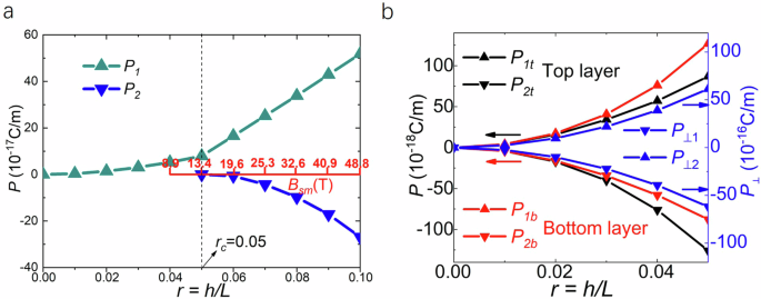
a In-plane flexoelectric polarization (P) for the rippled monolayer. The red axis in the middle indicates the corresponding maximum values of the pseudomagnetic field ({B}_{{rm{sm}}}) at different r. The vertical dashed line indicates the critical ripple strength rc. b In-plane flexoelectric polarization (P) (black lines for the top layer and red line for the bottom layer) and out-of-plane polarization ({P}_{perp }) (blue lines) for the rippled bilayer.
Multiferroicity in rippled monolayer and bilayer
So far, the coexistence of the pseudomagnetism and flexoelectricity has been demonstrated in both the rippled monolayer and bilayer, which undoubtedly endows these systems with the exotic property of multiferroicity. According to the common multiferroic classification, these rippled graphene layers belong to the so-called type-II multiferroics44,45,46, in which some magnetic orders can induce ferroelectricity or electric polarizations can cause magnetism. The direct coupling between the magnetic order and electric polarization in the type-II multiferroics provides a possibility for mutual manipulation of magnetoelectricity.
To elaborate more about the multiferroicity in the rippled graphene systems, we further investigate the relations between the PMF and electric polarization, especially with different strengths of the ripples. For the rippled monolayer, the effect of the PMF on the flexoelectric polarization is illustrated in Fig. 5a. The flexoelectric polarization is shown to slowly increase with the ripple strength when (r ,<, {r}_{c}=0.05), namely, the PMF is very weak. In this case, the flexoelectric polarization is not caused by the PMF, indicating that the system is not type-II multiferroic. When the PMF is strong enough (({r} ,>, {r}_{c})), the region of the original flexoelectric polarization is divided into two regions with opposite polarized directions, whose polarization values increase with the PMF (see ({P}_{1}) and ({P}_{2}) in Fig. 5a), enabling the system to exhibit multiferroicity. It is noted that the ripple strain can naturally give rise to flexoelectric polarization, but the PMF is uniquely responsible for the reversal of flexoelectric polarized direction.
As for the rippled bilayer considered, since the ripple strengths are not larger than ({r}_{c}), the above reversal of polarized direction does not take place in either layer of the rippled bilayer. Instead, the in-plane flexoelectricity and out-of-plane polarizations are simultaneously generated. Figure 5b shows that the in-plane (({P}_{b}), ({P}_{t})) and out-of-plane (({P}_{perp })) local polarizations can be tuned by the ripple strength. Intriguingly, the out-of-plane polarization is caused by the sublattice polarization originating from the interplay between the interlayer-coupling-induced polarization and intralayer-hopping-induced (PMF-induced) polarization, leading to the multiferroic nature in the bilayer.
Overall, the PMF can control the reversal of flexoelectric polarized direction in the rippled monolayer and the out-of-plane polarization in the rippled bilayer, contrary to the electric-field manipulation of the ferromagnetic–antiferromagnetic transition in FeRh71,72,73. In fact, the multiferroicity of ferroelectricity and magnetism in graphene has been reported. For example, it can be realized in pristine graphene with magnetic adatoms74 and in hydrogenated graphene bilayers75. Moreover, the coexistence of various orders has also been demonstrated in other 2D van der Waals materials76,77. Therefore, given that the multiferroicity of the PMF and flexoelectric polarization in few-layer rippled graphene originates from the non-uniform strain, we believe that their coexistence and interplay can not only lead to a renewed understanding of the diversity of flexoelectricity in graphene and explain related new phenomena observed in experiments, but also pave the way for application of the multiferroicity in magneto-electric functional devices, such as nanogenerators, miniature self-powered electronic devices, and for environmental detection under stress.
Discussion
In conclusion, we have demonstrated for the first time the coexistence of pseudomagnetism and flexoelectricity and their interplay in both the rippled graphene monolayer and bilayer. For the rippled monolayer, we showed that the non-uniform strain induces the spatial-dependent PMF, which can further cause a reversal of flexoelectric polarized direction over the critical ripple strength. The novel mechanism of such a transition, as identified here, provides a pathway towards realizing polarization phase switching in graphene. For the rippled bilayer, we revealed that the interplay of the interlayer coupling and intralayer hopping (or strain fields) makes the PMF to be enhanced in some regions of one layer and disappear in the corresponding region of the other layer. Intriguingly, besides the in-plane flexoelectric polarization, the rippled bilayer also exhibits the out-of-plane polarization, which can be effectively tuned by the in-plane polarization. The coexistence and interplay of pseudomagnetism and flexoelectricity presented here, known as type-II multiferroics, effectively modulate the polarization patterns, offering an appealing way to achieve novel functionalities in few-layer graphene. The main concepts and findings revealed for the graphene systems are also expected to be broadened to other 2D systems, with system-specific variations.
Methods
Tight-binding (TB) model for rippled graphene monolayer
In this work, we choose the nearest-neighbor TB Hamiltonian for a graphene monolayer as ({H}_{{rm{ML}}}=-sum _{ < {ij} > }{t}_{{ij}}{a}_{i}^{dagger }{b}_{j}+text{H.c.}), where ({a}_{i}^{dagger }) and ({b}_{j}) are the creation and annihilation operators on the A and B sublattices, respectively, and ({t}_{{ij}}) is the hopping parameter between the nearest-neighbor sites i and j. Note that, as described in Supplementary Note 1, the nearest-neighbor TB model, ignoring the other longer-range hopping terms, can largely capture the electronic properties of the rippled graphene. For pristine graphene, ({t}_{{ij}}={t}_{0}=-2.7) eV, while in the weakly deformed lattice9,15, ({t}_{{ij}}={t}_{0}+frac{beta {t}_{0}}{{a}^{2}}{left|{vec{delta }}_{{ij}}right|}^{2}nabla cdot vec{u}left(vec{r}right)), where ({vec{delta }}_{{ij}}) is the nearest-neighbor vector between the sites i and j, (beta approx 2 sim 3) is the electron Grüneisen parameter9, (a=1.42,mathring{rm A}) is the carbon-carbon bond length in pristine graphene, and (vec{u}left(vec{r}right)) is a displacement field in the deformed lattice. Given that pristine graphene grown on uneven or flexible substrates often exhibits one-dimensional (or quasi-) periodic ripple structures15,16, here we consider such one-dimensional ripples, whose shape can be approximately described by the function15 (Hleft(yright)=hsin left(frac{2pi y}{L}right)), with h and L being the height and period of the ripples, respectively, as illustrated in Fig. 1. Thus, the displacement field of the ripple, which varies along the y direction in the form of a cosine function, is (vec{u}left(vec{r}right)=left({u}_{x},{u}_{y}right)=left(0,tfrac{a}{2}{left[{H}^{{prime} }left(yright)right]}^{2}right)=left(0,frac{2{pi }^{2}{h}^{2}a}{{L}^{2}}{cos }^{2}left(frac{2pi y}{L}right)right)). The strain tensors in terms of the in-pane displacement (vec{u}left(x,yright)) are defined as15 (left{begin{array}{l}{u}_{{xx}}=frac{partial {u}_{x}}{partial x}+frac{1}{2}{left(frac{partial H}{partial x}right)}^{2},\ {u}_{{yy}}=frac{partial {u}_{y}}{partial y}+frac{1}{2}{left(frac{partial H}{partial y}right)}^{2},\ {u}_{{xy}}=frac{1}{2}left(frac{partial {u}_{x}}{partial x}+frac{partial {u}_{y}}{partial y}right)+frac{1}{2}frac{partial H}{partial x}frac{partial H}{partial y}end{array},right.). By neglecting the in-plane deformation, the strain tensors can be approximately expressed as (,left{begin{array}{l}{u}_{{xx}}approx 0,\ {u}_{{yy}}approx frac{2{pi }^{2}{h}^{2}}{{L}^{2}}{cos }^{2}(frac{2pi y}{L})\ {u}_{{xy}}approx 0,end{array},right.). Given the effective gauge field induce by the non-uniform strain field10,15,17, (left({A}_{x},{A}_{y}right)=-frac{beta hslash }{2{ea}}left(left({u}_{{xx}}-{u}_{{yy}}right),,-2{u}_{{xy}}right)=left(frac{beta hslash }{{ea}}frac{{pi }^{2}{h}^{2}}{{L}^{2}}{cos }^{2}(frac{2pi y}{L}),0right)), the generated PMF should be along the z direction and is given by ({B}_{s}=-frac{beta hslash }{{ea}}frac{2{pi }^{3}{h}^{2}}{{L}^{3}}sin (frac{4pi y}{L})), which is derived from the relation of B = ∇ × A.
TB model for rippled graphene bilayer
For the AB-stacked graphene bilayer (see Fig. 3), the TB Hamiltonian with the nearest-neighbor intralayer and interlayer hoppings is ({H}_{{BL}}=-sum _{left{ < {ij} > ,m=b,tright}}{t}_{m,{ij}}{a}_{m,i}^{dagger }{b}_{m,j}+sum _{j}{t}_{perp ,j}{a}_{t,j}{b}_{b,j}^{dagger }text{+H.c.}), where (m) is the index for the bottom ((b)) or top ((t)) layer, and ({t}_{perp ,j}) is the nearest-neighbor interlayer hopping parameter depending on the interlayer distance ({d}_{j}). The quantitative relationship between ({t}_{perp ,j}) and ({d}_{j}) can be determined by using the DFT calculations and maximally-localized Wannier functions, following the equation ({t}_{perp ,j}={t}_{perp }{e}^{-alpha frac{{d}_{j}-{d}_{0}}{{d}_{0}}}) (see Supplementary Note 8). Here, ({t}_{perp }=0.4) eV is the nearest-neighbor interlayer hopping parameter in the pristine graphene bilayer, corresponding to the equilibrium interlayer distance ({d}_{0}=3.25mathring{rm A}), and (alpha) is a decay factor.
TB electronic property calculations
The TB band structures were calculated through the diagonalization of the matrix of the Hamiltonian in k space. The local density of states (LDOS) was obtained from the imaginary part of the Green’s function (Gleft(omega right)={left(omega +ieta -Hright)}^{-1}), with the LDOS on site j given by ({rho }_{j}left(omega right)=-frac{1}{pi }text{IM}{G}_{{jj}}left(omega right)). Here, we set (eta =0.01). By integrating the LDOS, we can obtain the charge distribution, and the charge on site j was calculated by ({C}_{j}=2{{int_{-infty }^{0}}}{rho }_{j}left(omega right)domega) (The factor of ‘2’ is due to the consideration of the spin). Here, we would like to emphasize that the tight-binding model used in this study, which has been widely adopted in rippled graphene11,15,16, can incorporates the substrate effects, including magnetism, as reflected in the variation of the hopping term ({t}_{{ij}}). This approach can be compared with that based on effective Hamiltonian near the Dirac point used in ref. 3, where the effects of lattice potential, substrate, and magnetism are explicitly treated separately.
DFT calculations
The DFT calculations were implemented in the Vienna ab initio simulation package (VASP)78,79. The exchange-correlation energy was treated within the projector augmented wave method80 in the form of Perdew-Burke-Ernzerhof (PBE)81. In consideration of the practicability of the DFT calculations, we chose the scale of ripples as (sqrt{3}atimes 150a), where (a=1.42mathring{rm A}). A 21 × 1 × 1 k-point mesh, an energy cutoff of 520 eV, and a 15(mathring{rm A}) vacuum along the z direction were used in self-consistent calculations.
Responses