Combustion-assisted low-temperature ZrO2/SnO2 films for high-performance flexible thin film transistors

Introduction
Flexible electronics have been applied to various fields, such as panel displays, sensors, and memory, leading to significant interest in new processing technologies and materials1,2. In particular, thin-film transistors (TFTs) are crucial components that enable the construction of electronic circuits on flexible substrates, and the development of TFTs with both high-performance and mechanical flexibility for flexible devices has been the subject of ongoing research in major areas3,4. Among several semiconductor candidates for flexible TFTs, polymers are known to have limitations due to their low mobility and poor environmental stability caused by H2O and O2, despite their low processing temperature and stable mechanical flexibility. In contrast, metal oxides have been considered prominent materials for TFT channels due to their high carrier mobility (even in the amorphous phase) and excellent optical transparency, attributed to their unique orbital structure and wide band gaps5. As a result, they have been recognized as attractive materials for the development of next-generation applications, such as high-resolution and high-frame-rate displays, as well as high-performance transparent and flexible electronics. In particular, interest in flexible oxide TFTs has notably increased with the development of flexible TFTs using a-IGZO, which has made significant advances in the active matrix display industry6. In the past few years, research on new metal oxides that do not include rare elements, such as In and Ga in a-IGZO, while achieving higher TFT mobility, has been gaining attention. Among various oxides, Sn-based oxides such as ITZO, IGTO, ZATO, and SnO2 have demonstrated good electrical performance with high mobility and potential as alternative materials for oxide TFTs7,8,9,10. Sn4+ has a similar electronic structure to In3+, is abundant and more cost-effective, so it can partially or completely replace In. Moreover, unlike Zn2+ (284.1 kJ/mol), which is speculated to cause instability in TFTs due to weak bonding with oxygen, Sn4+ (531.8 kJ/mol) demonstrates high bonding energy with oxygen11. SnO2 can be a promising candidate due to its higher intrinsic mobility (250 cm2/Vs at 300 K) and wider bandgap (3.6 eV) compared to representative binary oxides such as In2O3 and ZnO, and it has the lowest melting point related to process temperature among these materials12. Furthermore, to clearly elucidate the enhanced performance of Sn-based oxide TFTs, it is necessary to research SnO2 as the starting material for these oxides.
From a processing perspective, oxide TFTs are compatible with various fabrication methods, suggesting that they can expand beyond conventional vacuum-based techniques to solution processes utilizing liquid sol–gel precursors such as spin coating, spray pyrolysis, and printing systems1,5. These processes offer advantages in cost-effective production over large areas compared to vacuum systems like sputtering and atomic layer deposition13. Since liquid precursors are used, it is possible to flexibly manipulate the composition of the sol–gel solution to obtain the desired characteristics of oxide films. Additionally, these techniques can be extended to oxide electrodes. In cases where ternary to quaternary compounds or doping are required, such as for oxide electrodes, different precursors can be combined to synthesize the solution, enabling the fabrication of fully solution-processed oxide TFTs. Despite the potential of the solution processes, the decomposition of organic ligands within sol-gel-processed oxide films and the dense structuring of metal oxide networks typically involves a high-temperature annealing process of 400 °C or higher, which is generally incompatible with flexible substrates14. Hence, various methods, including UV or laser annealing, O2 annealing, and aqueous solvents, have been explored to form solution-processed oxide films at low temperatures, ensuring film quality and meeting the thermal requirements with flexible substrates15,16,17,18,19. These methods utilize processes such as changes in the energy source, selective energy delivery to localized areas, and reduction of the conversion temperature to oxides. Among these methods, combustion synthesis is a chemical process that utilizes the internal energy generated through the exothermic reaction of added organic fuel and oxidizer in the precursor, allowing for the elimination of organic residues and promoting the transition to oxide films even at reduced external temperatures20. This approach enables the production of high-quality oxide films at low temperatures without requiring extra systems. Additionally, it offers the flexibility to modify the composition of the solution or integrate it with other low-temperature fabrication methods for additional effects. In our previous studies, we manufactured SnO2 TFTs using a combustion-assisted sol–gel process, achieving both oxide film formation and chlorine doping effect at low temperatures (~250 °C) by adjusting the composition of the solution used in the synthesis11,12. These results are compatible with flexible substrates, unlike Sn-based TFTs previously reported to be fabricated using the combustion process, which requires process temperatures of >350 °C21,22,23. Therefore, combustion synthesis can be a promising low-temperature sol–gel process for flexible SnO2 TFTs.
SiO2 has been widely used as the gate dielectric in most oxide TFTs due to its wide bandgap and amorphous state, resulting in extremely low gate leakage current. However, these TFTs have faced operational difficulties at low driving voltages due to the low dielectric constant of SiO224. Furthermore, the thinning of the gate dielectric with the scaling down of electronic devices has led to high gate leakage currents. This has made it challenging to apply them to next-generation flexible devices that require both high-performance and low power consumption25. To address these challenges, high-k dielectrics, which allow a reduction in operating voltage and high-density carrier accumulation through high capacitance values, have been proposed as new dielectric layers26. Among them, sol–gel-processed high-k oxides can be attractive alternatives, as they enable low-voltage operation and share the manufacturing process with sol–gel-processed oxide semiconductors. While various high-k oxides such as Al2O3, ZrO2, HfO2, and Y2O3 have been reported to be manufactured through solution processes24,27,28,29, ZrO2 has the potential to serve as an insulating layer in oxide TFTs for low-power operation due to its high dielectric constant (>20), sufficient bandgap (~5.8 eV), and electrical/chemical stability30. Furthermore, Zr4+ (760 kJ/mol) demonstrates stronger bonding with oxygen compared to Al3+ (511 kJ/mol), which allows for the formation of more complete metal-oxygen bonds and enables a reduction in interface trap sites between the insulator and the semiconductor31,32. The oxygen vacancy within high-k dielectrics can serve as a source of carrier trap sites, leading to decreased mobility of TFTs or causing shifts in threshold voltage and increased gate leakage currents33. In particular, ZrO2 has shown good compatibility with SnO2 semiconductors, and previous ZrO2/SnO2 TFTs manufactured through solution processes exhibited excellent dielectric-semiconductor interface properties and high electron mobility34. However, to obtain high-quality ZrO2 films, high-temperature annealing (>400 °C) was still required. To fabricate ZrO2/SnO2 TFTs on flexible substrates, both SnO2 and ZrO2 need to be manufactured using low-temperature solution processes. As mentioned earlier, we fabricated SnO2 TFTs using combustion-assisted solution processes in our previous work. Combustion synthesis can be applied not only to SnO2 but also to ZrO2 for manufacturing at low temperatures. Moreover, the combination of ZrO2 dielectric and SnO2 semiconductor fabricated from the same combustion materials enables the realization of sol-gel processed flexible oxide TFTs, while reducing processing times and costs.
In this paper, we report on high-performance flexible oxide TFTs realized with a SnO2 semiconductor and high-k ZrO2 dielectric formed at low temperatures using a combustion-assisted sol-gel process. Using the same approach as for the combustion of SnO2 films, ZrO2 films were formed at low temperatures. The external process temperature required to form the oxide network was estimated from thermogravimetric analysis (TGA). The structural and chemical composition differences of the prepared ZrO2 films were confirmed by grazing incidence X-ray diffraction (GIXRD) and X-ray photoelectron spectroscopy (XPS). Compared to conventional ZrO2 films, combustion films show an amorphous structure with a higher proportion of oxygen corresponding to the oxide network. These characteristics contribute to the low leakage current density and frequency-independent dielectric properties of combustion ZrO2 films. We fabricated flexible ZrO2/SnO2 TFTs using combustion synthesis, and the fabricated flexible TFTs exhibited a field-effect mobility of 26.16 cm2/Vs, a subthreshold swing of 0.125 V/dec, and an on/off current ratio of 1.13 × 10⁶ at a low operating voltage of 3 V. Furthermore, we compared the changes in electrical characteristics during repetitive bending tests to confirm the impact of scaling effects on the mechanical flexibility of the TFTs. As the device dimensions decreased, the deterioration of electrical characteristics after bending tests was reduced, and stable TFT operation was observed even after 5000 cycles of bending tests with a bending radius of 2.5 mm. This is because relatively small devices are less likely to contain structural defects or microcracks induced by mechanical stress.
Results and Discussion
Design for combustion synthesis
In our previous work, we successfully deposited SnO2 films at low temperatures using combustion synthesis and fabricated SnO2 TFTs on Si/SiO2, demonstrating enhanced TFT performance11,12. Thermal analysis confirmed that the external temperature required for precursor conversion was 250 °C, significantly lower than that of conventional precursors. XPS spectra showed that the combustion SnO2 films had a more complete metal oxide network compared to conventional SnO2 films. Consequently, the combustion SnO2 TFTs exhibited significantly improved electrical performance compared to conventional SnO2 devices, with mobility increasing by approximately 170 times from 0.014 to 2.43 cm2/Vs and the subthreshold swing decreasing from 3.85 to 1 V/dec. This suggests the potential for the full realization of sol–gel processed SnO2-based flexible TFTs, where low-temperature processes are required.
Figure 1 illustrates the process of forming ZrO2/SnO2 films from combustion solutions. We prepared ZrO2 solutions using a combustion system similar to that of SnO2. To synthesize these combustion ZrO2 solutions, Zr(C5H7O2)4 was employed as the Zr source, while NH4NO3 and CO(NH2)2 were used as the oxidizer and fuel, respectively. For conventional ZrO2 films, high-temperature annealing is required because endothermic reactions dominate conventional sol–gel processed metal oxides. In contrast, combustion synthesis requires less external energy supply for the decomposition of organic ligands and the construction of oxide lattices due to the internally generated energy from exothermic reactions, compared to the conventional ZrO2 system. Therefore, combustion ZrO2 films can be manufactured at lower temperatures.

Schematic diagram illustrating the process for forming ZrO2/SnO2 films using combustion solutions.
Characteristics of ZrO2 films
Figure 2a depicts the TGA curves of both ZrO2 precursors, enabling an assessment of the energy necessary for their conversion to oxides. In TGA curves, the conversion temperature of the precursors is determined from the temperature range where the weight stabilizes with minimal changes. The combustion precursors experience a sharp drop of about 20% in weight at approximately 230 °C, followed by relatively minor weight changes. Conversely, conventional precursors display comparable curves below 200 °C but exhibit a gradual weight reduction without distinct variations. Hence, from the TGA curves, it is discernible that combustion precursors primarily undergo conversion around 230 °C, whereas conventional precursors necessitate temperatures exceeding 400 °C. The TGA analysis indicates that the conversion of precursors in the combustion system occurs at significantly lower temperatures compared to conventional counterparts. This temperature difference suggests a reduced demand for external energy during oxide conversion, owing to the internal energy generated by the exothermic reaction of the combustion precursors. Using the conversion temperature obtained from thermal analysis as a reference, we determined that effective conversion into ZrO2 films could occur at 250 °C, similar to combustion SnO2. Furthermore, we anticipate that the resulting 2-terminal ZrO2 devices may demonstrate enhanced performance compared to those produced using conventional precursors, which necessitate high-temperature annealing. Additional details regarding these expected results will be elaborated upon in the following section dedicated to electrical characteristics.
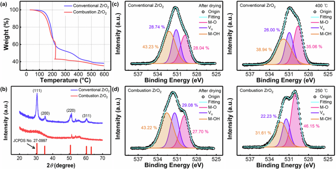
a TGA spectra of ZrO2 precursors with and without combustion materials. b GIXRD spectra of ZrO2 films prepared from different precursors. XPS O 1 s spectra of c conventional and (d) combustion ZrO2 films after the drying and annealing process.
The structural characteristics of the ZrO2 films used as the dielectric in transistors have a significant impact on the gate leakage current of the fabricated devices. In particular, in polycrystalline dielectric layers, grain boundaries can lead to ion diffusion and act as leakage paths, potentially contributing to a significant increase in leakage current35,36. The GIXRD spectra obtained for the structurally analyzed ZrO2 films are presented in Fig. 2b. Both ZrO2 films exhibit minor peaks associated with the monoclinic structure in the range of 50 to 60 degrees. The combustion ZrO2 films do not show noticeable peaks in the provided GIXRD spectra, indicating an amorphous state. In contrast, the conventional ZrO2 films annealed at 400 °C exhibit distinct peaks indicative of the cubic structure of ZrO2 (JCPDS No. 27-0997). The peaks at 30.5°, 35.2°, 50.7°, and 60.3° imply the (110), (200), (220), and (311) crystal planes, respectively. As a result, they exhibit a polycrystalline structure with clear peaks, distinguishing them from combustion ZrO2 films. The combustion ZrO2 films subjected to 250 °C annealing reveal an amorphous state with no significant peaks, suggesting that low-temperature annealing presents obstacles to the crystalline growth of ZrO2. Considering these findings, combustion ZrO2 films with an amorphous state, compared to high-temperature annealed crystalline ZrO2 films, can contribute to suppressing the increase in leakage current associated with the grain boundaries.
We conducted an XPS analysis to investigate the changes in the oxygen composition of ZrO2 films prepared using conventional and combustion precursors. The O 1 s spectra of the obtained ZrO2 films are shown in Fig. 2c, d. These spectra have been separated into three binding energies at 529.9, 531.3, and 532.2 eV, corresponding to metal-oxygen lattice (M-O), oxygen vacancy (Vo), and metal hydroxide (M-OH) groups37. Within solution-processed dielectrics, M-OH serves as an intermediate species that occurs before the formation of oxides. Therefore, a high M-O ratio indicates the formation of a more complete oxide lattice, while a high M-OH ratio suggests incomplete precursor conversion due to inadequate energy supply. Additionally, they can act as trap sites, and dipolar groups like -OH often lead to frequency-dependent capacitance characteristics of dielectrics at low frequencies, along with impurities and mobile ions (H+)38. Also, Vo is closely related to the increased leakage current characteristics of the insulator39,40. Regardless of combustion synthesis, the dried ZrO2 films before thermal annealing exhibit low M-O, high Vo, and high M-OH ratios, indicating that insufficient thermal energy led to the incomplete formation of an oxide network. This is because the drying temperature (150 °C) is not high enough to induce the combustion reaction. As observed in the TGA analyses, the conversion temperature of the combustion precursors is 230 °C, which is higher than the drying temperature. Therefore, the combustion reaction is not triggered during the drying process, resulting in incomplete conversion to the oxide film and no significant difference in oxygen composition. Additionally, below 200 °C, both precursors exhibit similar weight loss curves, which is consistent with these results. After annealing, both ZrO2 films show an increase in the M-O ratio and a decrease in the Vo and M-OH ratios compared to after drying. In particular, despite low-temperature annealing, the combustion ZrO2 films exhibit a higher M-O ratio, increasing from 35.06 to 46.15%, and lower Vo and M-OH ratios compared to the conventional ZrO2 films annealed at 400 °C. These changes imply that ZrO2 films manufactured through combustion synthesis establish a more complete oxide network even with low-temperature annealing. This phenomenon can be attributed to the chemical energy released in the exothermic reaction of combustion precursors, facilitating precursor conversion and the condensation reactions between M-OH for oxide lattice formation even at low temperatures. Through previous TGA analysis, we confirmed that the conversion of combustion precursors mainly occurs at a much lower temperature, around 230 °C, compared to conventional systems. The TGA analysis aligns well with the XPS results of combustion ZrO2 films, showing a more complete oxide network along with a high M-O ratio.
Dielectric properties of ZrO2 films
We manufactured metal-insulator-silicon (MIS) devices based on conventional and combustion ZrO2 to investigate the impact of combustion synthesis on the dielectric properties of ZrO2 films. Figure 3a presents leakage current density versus electric field plots for both conventional and combustion ZrO2 devices. The detailed leakage current density as a function of the electric field is summarized in Supplementary Table 1. The conventional ZrO2 films exhibit a breakdown field of ~3.1 MV/cm and leakage current density of ~2.82 × 10⁻⁷ A/cm2 at 1 MV/cm. However, the ZrO2 films obtained through combustion synthesis show a significant increase in breakdown field to ~8.3 MV/cm, approximately 2.7 times higher, and a substantial reduction in leakage current density to ~3.06 × 10⁻⁹ A/cm2, roughly 1/100 of the previous value, at 1 MV/cm. These values can be compared with previously reported vacuum-processed oxide dielectrics, which demonstrated excellent insulating capabilities41,42,43. Figure 3b, c depict dielectric constant versus frequency curves and the variation of dielectric constants as a function of the frequency of ZrO2 films. The conventional ZrO2 films exhibit a high frequency dependence of dielectric constants, particularly in the low-frequency range of 20 to 103 Hz. In contrast, the combustion ZrO2 films show a dielectric constant of 13.22 ± 0.43 at 20 Hz and a stable distribution of dielectric constants across the entire frequency range of 20 to 106 Hz. The decrease in dielectric constants across the whole frequency range is 7.6% for the combustion ZrO2 films, whereas it is 33.78% for the conventional ZrO2 films, which is a notable difference. The statistical results and detailed values of dielectric constants as a function of frequency are shown in Fig. 3d and Supplementary Table 2. Supplementary Table 3 summarizes our results and the characteristics of ZrO2 dielectrics prepared using conventional vacuum deposition. The combustion ZrO2 films exhibited properties such as low leakage current density and frequency-independent dielectric constants, making them comparable to previously reported vacuum-processed ZrO2 films. The conventional ZrO2 films, exhibiting high frequency dependence, also show high dielectric constants at low frequencies, attributed to their higher M-OH ratio, which allows for easy absorption of highly polar water molecules44. These insulation and dielectric constant-frequency characteristics suggest that the combustion ZrO2 films exhibit excellent dielectric properties in contrast to the conventional films annealed at high temperatures. Based on the GIXRD spectra, it was verified that the conventional ZrO2 films exhibit a polycrystalline phase, while the combustion ZrO2 films consist of an amorphous phase. As previously noted, the increase in leakage current associated with grain boundaries can be alleviated by the presence of the amorphous phase. Moreover, XPS results indicated that Vo, associated with increased leakage current, is suppressed. Consequently, high-quality ZrO2 films with a high M-O ratio were formed through the energy released from the combustion reaction. As a complete metal-oxygen network is established, the frequency dependence in capacitance induced by M-OH groups also decreases. Therefore, combining these film properties, combustion ZrO2 films demonstrate enhanced dielectric properties compared to conventional films annealed at 400 °C.
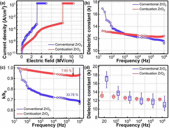
a Leakage current vs. electric field. b Dielectric constant, (c) variation in dielectric constant, and (d) statistical results of dielectric constant versus frequency (20 – 106 range).
Electrical characteristics of ZrO2/SnO2 TFTs
After verifying the dielectric properties of the fabricated combustion ZrO2 films, we proceeded to manufacture oxide TFTs capable of low-temperature and low-voltage operation using combustion SnO2 films. Figure 4 shows the schematics and electrical curves of the prepared TFTs. The transfer and output characteristics of combustion ZrO2/SnO2 TFTs are shown in Fig. 4b, c. The TFTs operate at a low driving voltage of 3 V with a low gate leakage current of ~10-9 A, demonstrating suitability for low-voltage operation oxide TFTs, owing to the prepared ZrO2 providing an amorphous phase and complete oxide network. The saturation mobility of ZrO2/SnO2 TFTs was extracted from the following equation,
where Ci, W, L, and Vth represent the capacitance per unit area of the insulator, channel width, channel length, and threshold voltage, respectively. When extracting mobility, we used the dielectric constant obtained at the lowest frequency we could measure, which is 20 Hz, to suppress any overestimating mobility. The high frequency dependence commonly observed in dielectric constants due to hydroxyl groups and mobile ions in solution-processed dielectrics can lead to an overestimation of mobility in TFTs with high-k dielectrics45. The fabricated ZrO2/SnO2 TFTs exhibited excellent electrical characteristics with a field effect mobility (({mu }_{{FE}})) of 22.3 ± 2.86 cm2/Vs, a subthreshold swing (SS) of 0.137 ± 0.013 V/dec, and an on/off current ratio (Ion/Ioff) of 5.8 × 10⁵. Detailed statistical distribution of TFT parameters is shown in Supplementary Fig. 3. The extracted ({mu }_{{FE}}) shows an improvement of about 10 times compared to the combustion SnO2 TFTs fabricated on 100 nm thick SiO2 layers in our previous work11,12. These results can be explained by the high carrier concentration achievable in the channel at low voltages due to high-k dielectrics, along with the shallow donor-like states in the ZrO2 layers that provide additional electrons46. As localized trap sites that hinder carrier transport become filled with accumulated carriers, it leads to improved mobility and better band-like transport of the ZrO2/SnO2 devices20,34. Generally, solution-processed oxide semiconductors exhibit amorphous or polycrystalline states, leading to localized trap states within the energy band and consequently following a trap-dependent multiple trapping and release (MTR) model47,48. However, when trap sites are filled, the transport mechanism transitions from MTR to a percolation conduction (PC) model, demonstrating band-like transport45. To verify the transport model governing the ZrO2/SnO2 TFT, the ({mu }_{{FE}}) was fitted to an integrated power-law equation including the gate voltage below:
where K and (gamma) correspond to the nature of carrier transport. Supplementary Fig. 4 shows the results of fitting the mobility of combustion ZrO2/SnO2 TFTs to the equation above. The value of (gamma) in the above equation provides insight into the dominant transport model for the respective oxide TFTs, with (gamma) values close to 0.7 and 0.1 in MTR and PC models, respectively47. Combustion ZrO2/SnO2 TFTs exhibit different (gamma) values at low and high VGS. At low VGS, the (gamma) for combustion TFTs was 0.70, while at high VGS, the (gamma) values were 0.12. The variation in (gamma) indicates the shift of dominant carrier transport from MTR to PC models as the gate voltage increases. The weak dependence of mobility on VGS also serves as evidence of the transition to the PC model. Additionally, the overestimated mobility obtained from conventional MOSFET analysis can be addressed by applying a scaling factor of (1/gamma +1), which reflects the transport models of metal oxides49. The accurate mobility of oxide TFTs can be derived by multiplying the mobility obtained through conventional methods by this scaling factor. The scaling factors for combustion ZrO2/SnO2 TFTs are 0.59 at low VGS and 0.89 at high VGS, respectively. Improved results are also observed in the SS, which is correlated with the trap density at the dielectric-semiconductor interface. As the dielectric layers shift from SiO2 to ZrO2, the average SS values show a steeper slope, from 1 to 0.137 V/dec. This suggests a lower trap density at the ZrO2/SnO2 interface, which is consistent with the significantly improved mobility observed in the ZrO2/SnO2 devices. The surface morphology of the combustion ZrO2 films obtained through atomic force microscopy (AFM) measurements can be seen in Supplementary Fig. 1e, and the root-mean-square (RMS) roughness of the prepared ZrO2 films was measured to be 0.563 nm, indicating a very smooth surface. This smoothness helps improve carrier transport and prevents degradation in device performance caused by rough dielectric-semiconductor interfaces. Electrical stability is also a crucial factor in TFT performance and should be considered for the practical use of solution-processed oxide TFTs. Figure 4d, e exhibit the transfer characteristics of the TFT under positive bias stress (PBS) and negative bias stress (NBS), while Fig. 4f shows the shift in Vth as a function of stress time. During the stress time of 3600 s considered for monitoring the stability of most oxide TFTs reported previously50,51,52, our device exhibited a shift of + 0.22 V under PBS and -0.18 V under NBS. The Vth shift induced by NBS can be seen to be relatively smaller compared to PBS. As seen in Fig. 4a, this is associated with the exposed SnO2 layers of the fabricated devices. Unlike NBS, which is primarily influenced by trap sites at the dielectric-semiconductor interface53,54, PBS is caused by oxygen species being absorbed through the back channel in ambient conditions55,56.
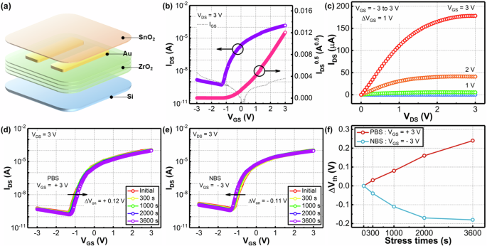
a Schematic diagram of the fabricated ZrO2/SnO2 TFT structures. b Transfer and (c) output characteristics of the devices. Transfer characteristics of the devices under(d) PBS, and (e) NBS. f Vth shift as a function of stress time under PBS and NBS.
Mechanical stability of flexible TFTs
After confirming the excellent electrical characteristics of ZrO2/SnO2 TFTs fabricated on rigid substrates, we proceeded to manufacture high-performance, low-voltage operation ZrO2/SnO2 TFTs on flexible substrates. We fabricated flexible ZrO2/SnO2 TFTs with various channel sizes and aligned the gate and source/drain (S/D) electrodes to minimize overlap during the fabrication process. The schematics and optical images of the prepared ZrO2/SnO2 TFTs can be seen in Fig. 5a, b, and detailed images for each channel size are shown in Fig. 5d–f. It is crucial for flexible TFTs to demonstrate stable electrical characteristics under mechanical stress. To compare the mechanical flexibility varying with the device’s dimensions, we applied repetitive tensile stress with a bending radius of 2.5 mm for 5000 cycles to the flexible TFTs, as shown in Fig. 5c, and observed changes in their electrical characteristics. The strain applied to our TFT structure can be estimated using the following equation:
where ({Y}_{{TFT}}) is distance from the bottom of the polyimide (PI) film to the center of the TFT layer, ({Y}_{c}) is the position of neutral plane for stacked films, and (rho) is the bending radius. The position of the neutral plane is calculated using the following equation57:
where ({E}_{i}) and ({t}_{i}) are the Young’s modulus and thickness of the i-th layer, respectively, and ({Y}_{i}) is the distance from the bottom of the stacked films to the center of the i-th layer. The Young’s modulus of each layer in the flexible TFT, based on previously reported values, is shown in Supplementary Table 4. The position of the neutral plane, calculated from these values, is ~26.93 µm from the bottom of the stacked films. The strain at the TFT location, estimated using equation (3), is approximately 0.53% with a bending radius of 2.5 mm.
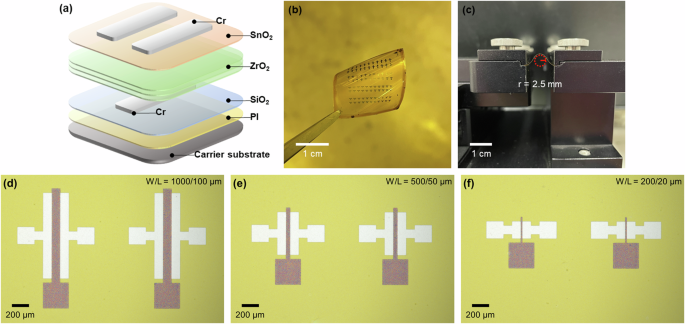
a Schematics of the fabricated ZrO2/SnO2 TFTs on PI substrates. b Optical images of flexible ZrO2/SnO2 TFTs. c Optical images of flexible TFTs in the bending state for mechanical stress testing. Optical microscopy images of flexible TFTs with different L: (d) 100, (e) 50, and (f) 20 μm, while maintaining a constant W/L ratio.
We successfully fabricated enhancement-mode flexible ZrO2/SnO2 TFTs on PI substrates. Figure 6a–c depicts the transfer characteristics of ZrO2/SnO2 TFTs with different channel sizes during the bending test, while Supplementary Table 5 shows the parameters of the flexible TFTs before and after the bending test. The fabricated flexible ZrO2/SnO2 TFTs (W/L = 200/20 µm) exhibited excellent electrical characteristics with a ({mu }_{{FE}}) of 26.16 ± 1.73 cm2/Vs, a SS of 0.125 ± 0.005 V/dec, and an Ion/Ioff of 1.13 × 10⁶, showing enhanced ({mu }_{{FE}}) compared to devices fabricated on rigid substrates. This improvement can be attributed to the increased charge carrier injection due to the change in the configuration of the flexible TFTs to bottom gate top contact, as opposed to the bottom gate bottom contact structure used in TFTs fabricated on rigid substrates. Additionally, the flexible ZrO2/SnO2 TFTs show a significant shift in Vth compared to the TFTs on rigid substrates and operate in enhancement mode. To elucidate the changes in operation modes, we obtained an energy band diagram, and Supplementary Fig. 5 illustrates the energy band diagram of the gate, ZrO2 dielectric, and SnO2 semiconductor. The position of the Fermi level (EF) within the energy band of the SnO2 film was estimated using the bandgap derived from the UV–vis spectra (Supplementary Fig. 5a) and the energy level difference between the EF and the valence band maximum (EVBM) obtained from the XPS spectra at the valence band region (Supplementary Fig. 5b). Subsequently, this was compared to the work functions of n++ Si and Cr when used as gate electrodes. From the energy band diagram in Supplementary Fig. 5c, d, these changes in Vth can be explained by the increased work function difference between the gate and the semiconductor, resulting from the change in the gate electrode of the flexible TFTs from n + + Si to Cr, compared to TFTs fabricated on rigid substrates.
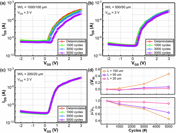
Transfer characteristics of ZrO2/SnO2 TFTs under bending stress for 5000 cycles at a 2.5 mm radius, varying with different L: (a) 100, (b) 50, and (c) 20 μm, while maintaining a consistent W/L ratio. d ({mu }_{{FE}}) and Vth variation under bending cycles.
The flexible TFTs exhibit variations in characteristics depending on the channel size. Shorter channel devices exhibit relatively decreased ({mu }_{{FE}}) compared to devices with longer channels, due to the influence of contact resistance58,59. Although these devices are fabricated from the same materials, as the channel length decreases, the channel resistance decreases, and consequently, the proportion of contact resistance in the total resistance increases. As a result, the effective voltage drop across the channel region decreases, leading to a decrease in ({mu }_{{FE}}). As the channel size decreases, a reduction in SS is observed, indicating an improvement in the quality of the interface between the semiconductor and insulator. Smaller TFTs can have fewer defects at the interface area, resulting in a reduction in trapped electrons at the interface trap sites60. The increased electrons lead to a negative shift in Vth, consistent with the decrease in Vth in the smallest devices. Furthermore, the reduced interface trap sites lead to a low off current61, thereby increasing the Ion/Ioff. The electrical characteristics of the fabricated flexible TFTs can be compared to previously reported vacuum or solution-processed high-k dielectric flexible oxide TFTs, and their mobility is fully compatible with state-of-the-art high-resolution active matrix displays (see Supplementary Table 6)62.
We investigated the mechanical properties of TFTs by comparing the electrical characteristics before and after the bending test, with particular attention to the scaling effect. As seen in Fig. 6 (a), TFTs with the largest channel sizes (1000/100 µm) clearly exhibit a decrease in on current along with the shift of the transfer curve during the bending cycles. Figure 6d and Supplementary Fig. 6 show the variations in TFT parameters depending on the bending cycles of devices with different channel sizes. Large-sized devices exhibit a noticeable decrease in ({mu }_{{FE}}) and a clear positive shift in Vth during bending tests. After 5000 cycles, Vth shifts positively from 1.27 to 1.65 V, and the ({mu }_{{FE}}) decreases to 46% of its original value, while SS increases from 0.148 to 0.154 V/dec. Repetitive bending cycles induce structural defects or microcracks in areas such as the gate dielectric-semiconductor interface or the gate electrode-gate dielectric interface where stress concentrates63. These changes can be explained by stress-induced structural defects trapping carriers at the ZrO2 and SnO2 interfaces. The increased interface trap density due to structural defects degrades the interface quality, reduces the carrier concentration in the channel region, and leads to the an increase in SS and a positive shift in Vth64,65. Additionally, from the perspective of the oxide carrier transport model (i.e. MTR), the increased localized trap sites hinder carrier transport, resulting in reduced ({mu }_{{FE}}) and degraded band-like transport. The accumulated defects during bending tests accelerate these changes. Also, microcracks formed during the bending test may propagate parallel to the bending direction, potentially leading to a decrease in mobility due to the presence of microcracks in the semiconductor layer64. However, as the channel size decreases, the shift in the transfer curve and performance degradation after the bending test are reduced, and in the TFT with the smallest size (see Fig. 6c), Vth barely changed from 1.04 to 1.09 V, while the mobility remained at 92% compared to before bending. Also, SS and Ion/Ioff show nearly constant values. This indicates that stable flexible TFTs have been implemented to withstand mechanical stress, suggesting that the dimensions of the devices influence the mechanical flexibility of TFTs. Relatively small-sized devices can withstand mechanical stress better compared to larger ones because it is more challenging for structural defects or microcracks induced by bending tests to be incorporated into the reduced insulating and channel regions. Furthermore, as seen in Fig. 5, the dimensions of the patterned electrodes, particularly the gate electrode, also decrease as the device dimensions decrease. Smaller patterned electrodes are less likely to develop microcracks under mechanical bending stress, thereby further enhancing the mechanical properties of the TFTs57. Supplementary Fig. 7 shows optical images of flexible TFTs after the bending test. Supplementary Fig. 7a shows microcracks induced by mechanical stress, which are more likely to be contained within the region of a relatively larger TFT. Additionally, as seen in Supplementary Fig. 7b, c, noticeable cracks due to bending stress are observed in larger gate electrodes compared to smaller ones, which correspond to changes in the mechanical properties depending on the electrode pattern size. Therefore, as seen in our results, as the dimension of devices decreases, the changes in transfer characteristics and main TFT parameters noticeably decrease. In particular, the smallest devices (200/20 µm) demonstrated robust mechanical stability, even under repeated bending stress, along with excellent TFT performance.
In this paper, we implement high-performance ZrO2/SnO2 TFTs on flexible substrates by combining SnO2 semiconductors and ZrO2 dielectrics obtained through a combustion-assisted sol-gel process. The internal energy generated from the oxidizer and organic fuel added for combustion synthesis aids in forming metal oxide networks even at low process temperatures. We fabricated ZrO2 films at low temperatures using the same approaches as for our previous combustion SnO2 films, and we confirmed the reduced conversion temperature compared to the conventional precursor through TGA. The GIXRD and XPS O 1 s spectra revealed that the combustion ZrO2 films exhibit an amorphous phase, with a low proportion of Vo and OH groups and a high proportion of oxygen corresponding to the metal oxide network. Two-terminal MIS devices fabricated with combustion ZrO2 exhibited higher breakdown voltages and lower leakage current density compared to conventional ZrO2 devices. Additionally, a lower frequency dependence of the dielectric constant was observed. This is attributed to the amorphous phase and decreased Vo and polar OH groups. The fabricated ZrO2/SnO2 TFTs on rigid substrates showed excellent electrical characteristics, including a ({mu }_{{FE}}) of 22.3 cm2/Vs, a SS of 0.137 V/dec, and an Ion/Ioff of 5.8 × 10⁵ at a low operating voltage of 3 V. These results can be explained by the better band-like transport resulting from the filling of localized trap sites with high-density carriers achieved at low voltages using high-k dielectrics. After confirming the promising TFT performance of ZrO2/SnO2 devices, we successfully realized enhancement-mode flexible ZrO2/SnO2 TFTs on PI substrates. The fabricated TFTs exhibited a ({mu }_{{FE}}) of 26.16 cm2/Vs, a SS of 0.125 V/dec, and an Ion/Ioff of 1.13 × 10⁶, showing enhanced ({mu }_{{FE}}) compared to devices fabricated on rigid substrates. This result can be explained by the increased work function of the gate electrode in flexible TFTs compared to those fabricated on rigid substrates, along with the structural change to bottom gate top contact, leading to increased carrier injection. We confirmed the scaling effect on the mechanical properties of TFTs by comparing the electrical performance through repetitive bending cycles. As the device dimensions decreased, the changes in transfer characteristics and performance degradation after bending tests reduced. This is because relatively small devices are less likely to contain structural defects or microcracks induced by mechanical stress. Furthermore, the smallest TFT demonstrated robust mechanical stability by withstanding 5000 cycles of bending tests at a bending radius of 2.5 mm. Therefore, combustion synthesis can be employed as a suitable process for the mass production of sol-gel process-based metal oxide electronic and flexible devices.
Methods
Synthesis of combustion ZrO2 and SnO2 precursors
We used ZrO2 and SnO2 precursors to form the dielectric and semiconductor layers of oxide TFTs. First, for the ZrO2 layers, we synthesized clear 0.1 M zirconium solutions by dissolving 0.001 mol of zirconium acetylacetonate (Zr(C5H7O2)4) in 10 ml of ethanol and subjecting it to ultrasonication for 1 h. The conventional ZrO2 films were obtained by annealing the zirconium solution without adding extra additives. Next, to prepare the combustion ZrO2 precursors, ammonium nitrate (NH4NO3) and urea (CO(NH2)2), serving as an oxidizer and fuel, were added to the prepared zirconium solutions, with 0.001 mol of each component. Since Zr(C5H7O2)4 does not contain NO3– ions to serve as an oxidizer, NH4NO3 containing NO3– was added. In a combustion system, the fuel is ignited by a relatively low level of external energy, providing internal chemical energy, and the NO3– contained in NH4NO3 acts as an oxidizer, leading to the activation of the combustion reaction, which is a form of redox reaction. Then, we stirred and aged the prepared combustion ZrO2 solutions at 80 °C for 48 hr to obtain a homogeneous yellowish solution. Next, the combustion SnO2 solutions were prepared using a process similar to that of ZrO2 solutions. Tin (II) chloride dihydrate (SnCl2·2H2O) was dissolved in ethanol to synthesize 0.04 M of SnO2 precursors. Then, NH4NO3 and CO(NH2)2 were added in a 1:1 ratio to SnCl2·2H2O as an oxidizer and fuel for the combustion precursors. Subsequently, the resulting solution was stirred and aged at room temperature for 72 h to obtain homogeneous combustion SnO2 solutions.
Fabrication process of ZrO2 devices and ZrO2/SnO2 TFTs
We manufactured 2-terminal ZrO2 MIS structures to measure the electrical properties of ZrO2 films. For the MIS devices, ZrO2 solutions were spin-coated onto heavily n-doped Si at 3000 rpm for 50 s, followed by 1 min drying at 150 °C to form the ZrO2 layers. This process was repeated to control the thickness of the ZrO2 layers. Before coating, the Si wafers underwent a 10 min UV/Ozone treatment for surface energy control. In addition to electrical characterization, we performed photopatterning to determine the thickness of the prepared ZrO2 films. Shadow masks were applied onto the dried ZrO2 layers and exposed to UV light for 10 min, followed by rinsing with DI water to pattern the ZrO2 films. The photopatterning of ZrO2 films is attributed to the photoreaction induced by UV irradiation of the metal precursors. In the UV-exposed areas, the precursors use light energy to form partial metal-oxygen bonds, whereas the unexposed areas, due to the shadow mask, do not undergo precursor conversion and are removed during rinsing with DI water. This results in the formation of ZrO2 patterns corresponding to the UV exposure. The prepared combustion ZrO2 films were annealed at 250 °C for 1 h, resulting in a film thickness of ~80 nm. Finally, top electrodes were deposited onto the patterned ZrO2 layers using a thermal evaporator to fabricate the MIS structures. The area dimensions of the top electrodes are 120 × 120 µm2 with a thickness of 50 nm. The details of the photopatterned ZrO2 films and MIS structure are shown in Supplementary Fig. 1.
The combustion ZrO2/SnO2 TFTs were fabricated through a process similar to the MIS structure. ZrO2 solutions were spin-coated onto heavily n-doped Si under the same conditions and annealed at 250 °C. Before forming the SnO2 layer, the S/D electrodes were patterned through a lift-off process. Au or Au/Cr layers were deposited using a thermal evaporator, and the resulting electrodes have a W and L of 1000 µm and 100 µm, respectively. The SnO2 films were formed by coating SnO2 solutions onto the ZrO2 at 3000 rpm for 50 s, followed by annealing at 250 °C for 1 h to manufacture the ZrO2/SnO2 TFTs. Before the annealing process, mechanical removal of the coated films along the deposited electrodes was performed to reduce fringe and leakage currents.
Fabrication process of flexible ZrO2/SnO2 TFTs
We fabricated flexible ZrO2/SnO2 TFTs on PI substrates. The fabrication process is as follows; Before coating PI, poly(vinyl alcohol) (PVA) was utilized as a sacrificial layer on the carrier substrate to facilitate easy detachment of PI. A solution prepared by dissolving 0.1 g of PVA in 40 ml of DI water was spin-coated onto the carrier substrate at 2000 rpm for 30 s and then dried at 110 °C for 90 s. Subsequently, the PI solution was spin-coated onto the PVA layer at 3000 rpm for 30 sec and dried at 90 °C for 5 min. This process was repeated to control the thickness of the PI layer, followed by annealing at 300 °C for 30 min for thermal solidification. The obtained thickness of PI was ~40 µm. Next, to compensate for the thermal mismatch between the PI layer and the ZrO2 layers, PECVD-SiO2 (100 nm) buffer layers were deposited, and Cr (50 nm) was deposited as the bottom gate electrode on the SiO2. Supplementary Fig. 2 illustrates the ZrO2 surface variation with the presence of a buffer layer. As shown in Supplementary Fig. 2a, cracks occurred during the annealing of ZrO2 coated on the PI substrate. This issue arises from thermal stress due to the mismatch in thermal expansion coefficients between the oxide films and polymer substrates66. To alleviate this thermal mismatch, we introduced SiO2, which had been used as a buffer layer in various oxide films, into our structure67,68,69. The ZrO2 surface annealed on top of the buffer layer showed a crack-free appearance, as depicted in Supplementary Fig. 2b. In bottom-gate structure TFTs, the requirement for the gate electrode is adhesion with the flexible substrate. Taking this into consideration, we chose Cr as the bottom gate electrode. Subsequently, the ZrO2 and SnO2 layers were deposited as the dielectric and semiconductor layers, respectively, and Cr (50 nm) was deposited as the S/D electrodes to fabricate bottom-gate, top-contact TFTs. To confirm the scaling effect, the sizes of the flexible TFT channels were prepared in three different sizes, maintaining a W/L ratio of 10 with L = 100, 50, and 20 µm. After the process, the PI film was immersed in DI water to dissolve the PVA and delaminate it from the carrier substrate.
Characterization of ZrO2 films and TFTs
The thermal behavior of the prepared ZrO2 precursors was analyzed using TGA (TA Instruments/Discovery SDT 650). TGA analyses were conducted on approximately 20 mg samples obtained from evaporated precursor solutions. The samples were heated at a rate of 10 °C/min with a 30 ml/min airflow using a platinum sample pan. The differences in crystallinity and structural characteristics of ZrO2 films fabricated from different precursors were determined using GIXRD (Panalytical/Empyrean) with Cu Kα radiation (λ = 1.54 Å). Surface morphology of the ZrO2 films and thickness measurements of the patterned ZrO2 films were performed using AFM (Park Systems/NX-10). XPS (Thermo Scientific/ESCALAB 250Xi) analysis with a monochromatic Al Kα (1488 eV) source was conducted to investigate the oxygen composition within the formed ZrO2 films. The electrical properties of the fabricated MIS devices and ZrO2/SnO2 TFTs were measured using the Keithley 4200-SCS analysis system inside a probe station.


Responses