Controllable half-metallicity in MnPX3 monolayer

Introduction
Spintronics, which is based on the spin degree of freedom, is a field of science and technology that will most likely have a significant impact on the future electronics. Among various spintronic materials, one of the most promising candidates is half-metal (HM)1,2, which has the ability to provide 100% spin-polarized electrons due to its special band structure, i.e., one spin channel is metallic and the other is semiconducting3,4,5,6,7. According to the previous reports, HM can be obtained in the semi-Heusler alloys8,9, the manganese perovskites10, and the oxides such as chromium dioxide and magnetite11,12,13, etc.
Recently, with the rapid development of two-dimensional (2D) materials14,15,16, many 2D HM has been reported17,18,19,20,21,22. One outstanding approach to obtaining 2D HM is based on a new type of semiconductor, i.e., bipolar magnetic semiconductor (BMS)23, whose conductance band minimum (CBM) and valence band minimum (VBM) have full spin polarization with opposite directions. In BMS, ±100% spin-polarized HM and the switching between them can be easily obtained by applying positive/negative gate voltage (hole/electron doping). In 2023, we reviewed the development of 2D BMS24. Until now, some intrinsic 2D BMS have been proposed, for example, 2H-VX2 (X = S and Se)25,26, GdI227 and NbS228, etc. To obtain more BMS, various approaches have been proposed to tailor BMS band structures29,30,31,32,33,34. For example, BMS can be obtained in 2D AFM by destroying the balance of the crystal field of the antiferromagnetically coupling magnetic ions35,36,37,38,39,40. A typical case is that 2D AFM semiconductor Cr2TiC2 becomes a BMS by adsorbing F and Cl atoms on its top and down surfaces, respectively35,36.
Layered transition-metal phosphorus trichalcogenides MPX3 (M = Mn, Fe, Ni, and V; X = S, Se, and Te)40 are an important family of materials that can be exfoliated in two dimensions. MnPSe3 monolayer has been characterized experimentally41, and has attracted much attention due to its excellent electrical and magnetic properties42,43,44,45. Interestingly, 2D MnPSe3 has achieved AFM-FM transition through strain38 or carrier doping39,40. In this work, we investigate the magnetic properties of MnPSe3 monolayer adsorbed by Li and F atoms and MnPS3 contacting with Au(111), using density-functional theory (DFT). We find that both MnPSe3 and MnPS3 monolayers can become half-metallic, due to the extra charge they obtain from surroundings.
Results
Ground states of MnPS3 and MnPSe3
Due to the weak interlayer van der Waals (vdW) force, 2D MnPX3 (X = S and Se) can be easily exfoliated41,46. The unit cell of the MnPX3 monolayer is composed of two Mn2+ and one [P2Se6]4+ cluster47. The side view of MnPX3 can be seen in Fig. 1a. We optimize the lattice structure of MnPX3 monolayer and obtain the lattice constants of MnPSe3 about 6.387 Å and MnPS3 about 6.080 Å, which are in good agreement with the experimentally reported values of 6.402 Å for MnPSe339 and 5.997 Å for MnPS340. Although FM MnPX3 shown in Fig. 1b is not the ground state, several approaches have been proposed to induce AFM-FM transition in MnPX3. For example, gate modulation through hole/electron doping can induce AFM-FM transition in MnPSe339. In addition, in the multiferroic MnPS3/Sc2CO2, AFM-FM transition in MnPS3 can be tuned by reversing the ferroelectric polarization direction of Sc2CO248. In Fig. 1c, we summarize the approaches that can induce AFM-FM transition in MnPX3, in which adsorption doping and metal contract will be discussed in our present work.

a, b The side views of AFM and FM monolayer MnPX3 (X = S and Se), in which the red/blue arrows represent the spin-up and -down, respectively. c The transition from AFM to FM MnPX3 by gate doping, multiferroic heterostructure, adsorption doping, and metal contact.
According to the calculation, the total energy of AFM MnPSe3 is lower than that of the FM state by about 40.10 meV/unit cell (u.c.). We plot the band structures of AFM and FM MnPSe3, as shown in Fig. 2a, b, respectively. We can see that the band gap of AFM MnPSe3 is obviously larger than that of FM MnPSe3. In addition, we notice that the CBM and VBM of FM MnPSe3 have the opposite spin polarization, which means that FM MnPSe3 is a BMS. Fig. 2c, d show the band structures of AFM and FM MnPS3, which are similar to MnPSe3. The total energy of AFM MnPS3 is lower than that of the FM state by about 54.77 meV/u.c.
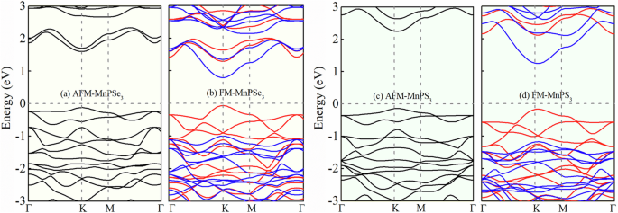
AFM and FM band structures of a, b MnPSe3 and c, d MnPS3. Blue and red represent spin-down and -up states, respectively.
Half-metallic ferromagnetism in the Li- and F-doped MnPSe3
In order to study the adsorption effects on the electronic structures of 2D MnPSe3, we construct 2 × 2 × 1 supercells, as shown in Fig. 3, in which solid blue circles represent the Li/F atoms and the red diamond indicates the unit cell of MnPSe3. Adsorption sites of Li/F on the top of P, Mn, and Se atoms are all considered. Fig. 3a–d shows the atomic structures of Li/F adsorption on the top of P atoms with concentrations of 25%, 50%, 75%, and 100%, respectively. The atomic structures of the MnPSe3 monolayer with Li/F atoms on the top of Se and Mn atoms can be seen in Figs. S1 and S2, respectively. According to the total energy, Li/F adsorptions on the top of P atoms are more stable.
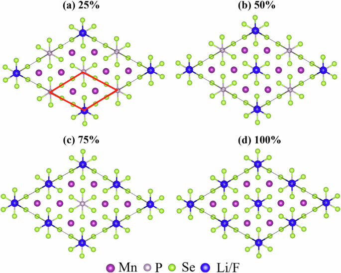
Atomic structures of MnPSe3 monolayer with different Li/F atoms adsorption concentrations: a 25%, b 50%, c 75%, and d 100%.
We also check the ground states of MnPSe3 with different adsorption concentrations. According to the total energy calculation, FM MnPSe3 is more stable with Li/F adsorption, as can be seen in Table 1. For the Li adsorption, ΔE is from 45.8 to 85.7 meV, and for the F adsorption, ΔE is from 28.8 to 155 meV. For both Li and F adsorptions, all the concentrations, including 25%, 50%, 75%, and 100%, can induce AFM-FM transition in MnPSe3. With the increasing concentration from 25% to 100%, the Bader charge linearly increases from 0.224 to 0.868 e/u.c. for the Li adsorption and −0.175 to −0.683 e/u.c. for the F adsorption. In the previous reports39, electron, and hole doping with the carrier concentration of 1.4 × 1014 cm−2 can induce AFM/FM transition in MnPSe3. It is clear that the Bader charge induced by the Li/F adsorption exceeds the electron and hole doping mentioned above.
Band structures of MnPSe3 monolayer with different Li/F concentrations are also calculated. As shown in Fig. 4a, b, the MnPSe3 monolayer has a complete spin-down polarization in blue with 25% and 50% Li concentrations and remains an HM. When the adsorption concentration increases to 75% and 100%, as shown in Fig. 4c, d, both spin-up and -down channels cross the Fermi Level and show metallicity. Fig. 4e–h shows the band structures of MnPSe3 with the F adsorption. It is clear that for all four concentrations, the F-adsorbed 2D MnPSe3 remains an HM. In summary, MnPSe3 can exhibit a complete spin-up polarization with the Li adsorption, and a full spin-down polarization with the F adsorption. When MnPSe3 is adsorbed with the Li atom, electrons will easily transfer from the Li atom to MnPSe3, i.e., MnPSe3 will gain electrons. It will gain more electrons with the increasing adsorption concentration, and the Fermi level will shift up into the conduction bands of MnPSe3. However, for the F atom adsorption, electrons will transfer from MnPSe3 to the F atom, and the Fermi level will shift down into the valence bands of MnPSe3.
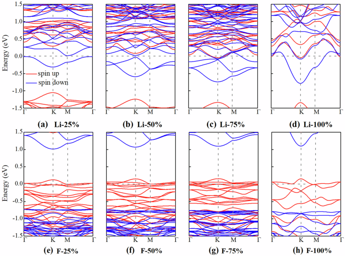
Band structures of MnPSe3 monolayer with different Li and F adsorption concentrations: a, e 25%, b, f 50%, c, g 75%, and d, h 100%.
The band structures of the MnPSe3 monolayer with Li/F adsorption on the top of Se/Mn atoms can be seen in Figs. S3 and S4. Other atoms, such as Ca, O, and Cl are also considered, as shown in Figs. S5 and S6. For all the adsorptions, we can obtain AFM-FM transition, which means that FM MnPSe3 can be easily obtained, and actually, it is an important spintronic material.
To well understand the AFM-FM transition induced by the adsorption, we perform density of states (DOS) calculations for the Li/F-adsorbed MnPSe3 with 50% concentration, as shown in Fig. 5. We plot the non-magnetic (NM) and FM DOS for comparison. For the NM DOS of both the Li/F-adsorbed MnPSe3, sharp peaks appear at the Fermi level, while for the FM DOS, the sharp peaks disappear. According to the Stoner criterion49,50, the extremely large DOS at the Fermi level cannot be stable, which will induce magnetic transition.
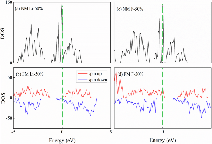
NM and FM DOS of MnPSe3 with 50% adsorption concentration: a, b Li adsorption and c, d F adsorption.
MAE is defined as the total energy difference between E[001] and E[100], i.e., MAE = E[001] − E[100]. The positive and negative MAE corresponds to the in-plane and out-of-plane magnetization easy axis, respectively. To obtain MAE, we include spin-orbit coupling (SOC) in the calculations51, and the results are shown in Fig. 6a. It is clear that the pure MnPSe3 with positive MAE has the in-plane magnetization axis. For the Li adsorption, the easy axis reverses from in-plane to out-of-plane, when the adsorption concentration is around 25%. In contrast, for the F atom adsorption, MAE of MnPSe3 remains positive for all the concentrations, i.e., the F-adsorbed MnPSe3 has the in-plane easy axis. In addition, we notice that the absolute value of MAE of the F-adsorbed MnPSe3 is much larger than that of the Li-adsorbed MnPSe3. This is because the 3d-orbitals of the Mn atom dominate the valence band maximum and they cross the Fermi level when F is adsorbed, while p-orbitals of the Se and P atoms dominate the conduction band minimum, and they cross the Fermi level when Li is adsorbed. Mn-3d-orbitals have a larger influence than p-orbitals of the Se and P atoms.
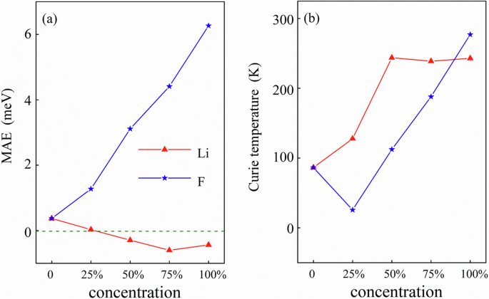
a MAE and b the Curie temperature of MnPSe3 with different Li/F adsorption concentrations.
We also calculate the total energy of FM, AFM-Néel, AFM-Zigzag, and AFM-Stripy MnPSe3 with different Li/F adsorptions, and obtain the parameters J1, J2, J3, and the Curie temperature. The structures of FM, AFM-Néel, AFM-Zigzag, and AFM-Stripy MnPSe3 are shown in the previous reports40. The relation between the adsorption concentration and the Curie temperature is shown in Fig. 6b. The Curie temperature of the pristine 2D MnPSe3 is about 86 K, which is in good agreement with the previous research (88 K)39, confirming the validity of our model. For the F adsorption, Tc increases with the adsorption concentration and nearly reaches the room temperature for 100% adsorption. For the Li adsorption, Tc can reach 240 K when the concentration is 50%, and it does not change for 75% and 100%.
Half-metallic ferromagnetism at the MnPS3/Au(111) interface
Since hole/electron doping can induce AFM/FM transition in MnPX3, contact with metal may also induce AFM/FM transition in MnPX3. In Fig. 7a, we schematically draw the field-effect transistor, which has the electrodes of Au(111) and transport material of MnPS3 monolayer. We construct the heterostructure MnPS3/Au(111), as shown Fig. 7b, to investigate the influence of the metal contact on the magnetic properties of MnPS3. The lattice constant of MnPS3 and Au(111) is 6.08 Å and 5.90 Å, respectively, resulting in a relatively small mismatch of about 2.96%. According to the structural relaxation, we get an interlayer space of about 2.40 Å between MnPS3 and Au(111). The planar average of the electrostatic potential energy of MnPS3 and Au(111) are shown in Fig. 8a and b, respectively, from which we can see that the work functions of MnPS3 and Au(111) are 5.871 eV and 5.825 eV, respectively. Since the work function of Au(111) is smaller, electrons will transfer from Au(111) to MnPS3, forming the Ohmic contact, which can also be confirmed in the band structure.
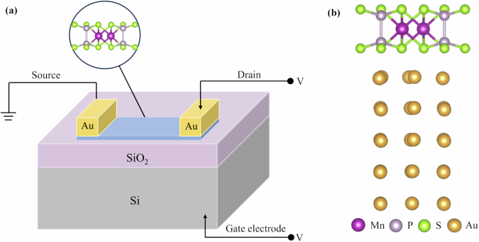
a The schematic field-effect transistor and b atomic structure of MnPS3/Au(111).
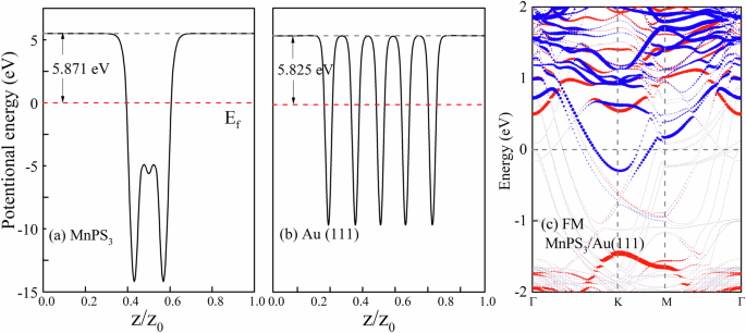
a, b The planar average potential energy of MnPS3 and Au(111), and c the band structure of FM MnPS3/Au(111).
We test the AFM and FM states for the heterostructure and find that the FM states have lower total energy. For each unit cell of the heterostructure, the energy difference (ΔE) between AFM and FM is about 22.5 meV. The calculated band structure of the FM MnPS3/Au(111) is shown in Fig. 8c, in which the atomic orbitals of MnPS3 are picked out and their weight is indicated by the circles in blue (spin-down) and red (spin-up). We can see that the Fermi level crosses the conduction band of MnPS3, which means that MnPS3 obtains electrons from Au(111), and the Ohmic contact is formed. In addition, we notice CBM of MnPS3 is fully spin-polarized in blue, which is consistent with the Li adsorption.
Discussion
Through first-principles calculations, we investigate the AFM/FM transition in monolayer MnPX3. We find that both the Li- and F-adsorbed MnPSe3 monolayers can become HM, and HM is well preserved for a large range of concentrations. The curie temperature and the magnetic anisotropy of the Li- and F-adsorbed MnPSe3 are calculated. It is found that the Curie temperature can be obviously enhanced by the adsorption (~240 K for the Li adsorption and ~280 K for the F adsorption). The magnetization easy axis of the Li-adsorbed MnPSe3 can switch from in-plane to out-of-plane, while that of the F-adsorbed MnPSe3 remains in-plane. In addition, in the heterostructure MnPS3/Au(111), charge transfers from Au(111) to MnPS3 and Ohmic contact is formed, and AFM/FM transition is also obtained.
Both adsorption and contact with metal surfaces commonly exist in devices, which, however, give rise to quantitative change for MnPX3. Our study shows that 2D MnPX3 can show ferromagnetic half-metallicity in reality, although it is intrinsically an antiferromagnet, which means that 2D MnPX3 can be regarded as an important spintronic material.
Methods
All calculations are based on the Vienna ab initio simulation package (VASP) in the framework of density-functional theory (DFT)52,53. The projector augmented wave (PAW) method and the Perdew–Burke–Ernzerhof (PBE) general functional with the generalized gradient approximation plus on-site Coulomb interaction U (GGA + U) with U = 5 eV46,54 is used. For the MnPSe3 monolayer, to avoid interactions between neighboring layers, 20 Å of vacuum space along the z-axis is inserted. A cutoff energy of 450 eV is set for the plane wave expansion. Monkhorst k-mesh grids of 8 × 8 × 1 and 4 × 4 × 1 are used for the Brillouin-zone sampling of 1 × 1 × 1 and 2 × 2 × 1 MnPSe3, respectively. For geometry optimization, all of the internal coordinates are relaxed until the Hellmann-Feynman force is less than 0.01 eV·Å−1 for each ion, and total energy convergence is within 10−5 eV.
Responses