Controlled layer-by-layer assembly and structured coloration of Ti3C2Tz MXene/polyelectrolyte heterostructures
Introduction
Two-dimensional (2D) transition metal carbides and nitrides (MXenes) have generated significant interest due to their potential use in electronics, optics, and robotics1. MXenes follow the chemical formula of Mn+1XnTz, where M is a transition metal, X is carbon and/or nitrogen, T represents a surface terminal group, z is the number of terminal groups, and n is a number 1–42. MXenes are known to offer a variety of desirable properties involving conductivity, hydrophilicity, and optical absorption3,4,5. Studies into the optical response of MXenes show that the intra- and interband transitions control the dielectric constant based on the terminal groups of the MXene6,7,8. Overall, Ti3C2Tz MXenes possess a high absorption coefficient throughout the UV, visible, and infrared ranges (i.e., anomalous dispersion at most wavelengths). Despite exhibiting appealing material characteristics, MXene nanosheets often have the propensity to restack9, which impedes control over the MXene’s nanostructure and can complicate subsequent material processing (e.g., into large-scale thin films and optical coatings).
Layer-by-layer (LbL) assembly potentially offers a means to control the spacing between MXene layers by depositing negatively charged MXene in a defined sequence with a complementary material (e.g., a polyelectrolyte). Using this approach, the resulting LbL assembly is stabilized by electrostatic attraction between the alternating positively charged and negatively charged layers10,11. Prior work has demonstrated MXene-containing LbL structures, including but not limited to, polydiallyldimethylammonium (PDADMA)/Ti3C2Tz films for humidity and pH sensors, silane-functionalized Ti3C2Tz/Ti3C2Tz films with improved conductivity, and nanomaterial/Ti3C2Tz coated electrodes12,13,14,15,16,17. LbL assembly is surface-agnostic in that coatings can be created on a variety of substrates (e.g., glass, fabric, carbon, nanoparticles, Teflon) using an assortment of materials (e.g., nanomaterials, polyelectrolytes)13,18,19,20. LbL assembly also allows for nanometer-level control layer thicknesses, which can be tuned based on the material composition, deposition time and method (e.g., dip-, spray-, spin-coating), and pH of solutions. For example, layer pairs (LPs) within LbL assembled films have been as thin as 2 nm and up to hundreds of nanometers in thickness10,21,22,23.
LbL assembly is promising for preparing optical coatings because the technique allows for precise control of each layer’s thickness and chemistry, yielding multilayer heterostructures for optical filters such as Bragg reflectors, omnidirectional absorbers, and gradient-index rugate filters24,25,26. For example, Puzzo et al. fabricated distributed Bragg reflectors from several material combinations of SiO2, TiO2, SnO2, and Sb:SnO2 nanoparticles23. Layer thicknesses varied from 60 nm to 287 nm, depending on the nanoparticle composition. The effective refractive index contrasts of the alternating material layers varied from 0.03 to 0.59, demonstrating different peak reflection intensities at visible wavelengths. Additionally, the reflected color was shown to differ with respect to changes in the reflection peak location. The observed coloration in these heterostructures stems from the phenomenon of structured color. Such color generation at visible wavelengths is due to light interactions within the structured nanoarchitecture (e.g., nanomaterial size, dimension, and geometry or aspect ratio in relation to the heterostructure architecture), rather than the use of organic pigments or dyes that absorb/reflect light of specific wavelengths based on the molecular composition and bonding configuration. Optical coatings and devices that make use of structural coloration do so by controlling the optical properties (i.e., the refractive index, n, and extinction coefficient, k) of the respective material layers and layer thicknesses. To date, MXene nanosheets have not been incorporated into LbL assemblies for structural color applications.
In past studies, MXenes have been primarily used as a base to amplify the structural colors of the materials above (e.g., SiO2 nanoparticles). For example, Xue et al. used blade-coated Ti3C2Tz MXene on a substrate to create a black background beneath layers of SiO2 nanoparticles27. Li et al. used MXenes as a support for the actuation of polystyrene photonic crystals28. Similarly, Bian et al. used MXenes as a support for bioinformation coding leveraging SiO2-dopamine photonic crystals29. Zhang et al. also used MXene as a black background for soft photonic crystals with electrochromic applications30. In each of these past works, MXenes did not contribute to the structural coloration itself; instead other photonic crystal materials were utilized.
Here, we propose that MXenes can be integrated into a heterostructure architecture via LbL assembly—potentially eliminating the need to incorporate other nanostructured materials (e.g., SiO2) to achieve the desired structured color behavior. Specifically, we report the LbL assembly of MXene/polyelectrolyte heterostructures using two different cation/anion LP sets (or blocks). These blocks are composed of PDADMA/Ti3C2Tz MXene and PDADMA/polystyrene sulfonate (PSS). PDADMA/PSS LbL multilayers have been previously studied and well characterized31,32,33,34,35,36, allowing us to focus on how the inclusion of the MXene-rich block contributes to the heterostructure’s structural color. Adjustments to the PDADMA/PSS block are made through varying salt concentration and number of layer pairs. This allows for the thickness of the PDADMA/PSS block to differ, thus altering the thickness between MXene-rich blocks. We investigate the impact of this spacing on the optical response, including structural color. The film morphologies and growth rates are also studied to demonstrate the potential range of control afforded by the LbL assembly technique. This study opens the door for LbL MXene-polymer configurations that can yield tailored wavelength-dependent optical performance (e.g., reflection, transmission, and absorptance) optical coatings for applications in actuation, thermal camouflage, and bioinformation coding.
Results and discussion
Three different compositions of LbL heterostructures were created to demonstrate control of the different block thicknesses. Figure 1a shows a schematic of the LbL films, where different sequences of LbL assembly are performed in blocks to create distinct repeating sections. Block A was composed of two LPs of PDADMA/Ti3C2Tz, and block B was composed of either two or four LPs of PDADMA/PSS assembled at 0.5 M NaCl. In a third set, block B contained two LPs of PDADMA/PSS assembled at 1.0 M NaCl. In all three sets, blocks of A and B were alternated “x” times to create heterostructures of various block pairs. As nomenclature, the LbL films are denoted as [(PDADMA/Ti3C2Tz)2/(PDADMA/PSS)m]x where the materials for each block are within parentheses, followed by a subscript that represents the number of layer pairs in said block. The “m” subscript following the PDADMA/PSS block will either be a 2 or 4, depending on the heterostructure system, while the “x” subscript following the end bracket represents the number of times the block pairs were repeated. If this value ends in .5, this means that the PDADMA/Ti3C2Tz block is on top of the heterostructure. For block A, citric acid was added to the assembly solutions to prevent MXene oxidation14,37,38. These three different LbL systems allowed us to analyze how changing the spacing between the MXene-containing blocks, through varying the thickness of polymer-rich block B, affected the heterostructure’s growth and optical properties. Each composition was made at least three times, and then the data were compiled and statistically analyzed.

a Schematic of the block and layer pair makeup for the heterostructures. b Cross-sectional SEM image of a [(PDADMA/Ti3C2Tz)2/(PDADMA/PSS)2]8.5 assembled with 1.0 M NaCl in block B. c AFM surface morphology of an LbL heterostructure, [(PDADMA/Ti3C2Tz)2/(PDADMA/PSS)2]x with 0.5 M NaCl in block B, where a MXene layer from block A is the outermost layer (left) and where PSS from block B is the outermost layer (right). d–f TEM images of varying magnifications of a [(PDADMA/Ti3C2Tz)2/(PDADMA/PSS)2]8.5 assembled with 0.5 M NaCl in block B. The orange line demarcates the platinum surface coating deposited to reduce charging, and the blue line demarcates the Si substrate. The material between the orange and blue lines represents the heterostructure cross section. The chartreuse brackets highlight darker regions attributed to MXene-rich block A, and the pink brackets highlight lighter regions attributed to polymer-rich block B.
Cross-sectional scanning electron microscopy (SEM) was performed to confirm the presence of the alternating blocks. Due to the thin blocks and the presence of polymer within the heterostructure, SEM imaging at high magnifications was difficult because of film charging. Films were freeze-fractured to produce a cleaner cross-sectional cut. The SEM image in Fig. 1b shows a cross-section of a [(PDADMA/Ti3C2Tz)2/(PDADMA/PSS)2]8.5 with 1.0 M NaCl in block B. The alternating layers of light and dark gray indicate the successful creation of a heterostructure morphology. The light gray areas correspond to the polymer-rich block B, and the dark gray areas correspond to MXene-rich block A. In the magnified inset, pieces of MXene nanosheet appear to protrude from the film, which we attribute to the sample preparation. Overall, Fig. 1b presents a representative morphology in which the other LbL systems investigated show a layered or “blocky” structure, see below.
Topographic scans were performed using atomic force microscopy (AFM) to compare the surface morphology of the terminating layers. Figure 1c left shows a topographical scan of an LbL heterostructure in which MXene nanosheets were the last material deposited. The observed wrinkling is a result of overlapping MXene nanosheets that lay atop one another. The sheets themselves were about 0.5 to 3.5 μm in lateral size38, which is on the order of the wrinkle’s features. Figure 1c right shows a similar scan in which PSS was the last material deposited. Similar to Fig. 1c left, the surface presents a wrinkled morphology over the area scanned (10 × 10 μm2). The roughnesses were comparable at 5.48 nm for when MXene was the last layer and 5.50 nm for when PSS was outermost. This result indicates that each layer deposits uniformly over one another and preserves the surface texture of the block or layer just beneath it.
Transmission electron microscopy (TEM) provides cross-sectional images of heterostructure morphology. Figure 1d–f displays distinct stripe-like layering in the LbL assembly, consistent with the layering observed in SEM images (Fig. 1b). The darker gray layers, as highlighted by the chartreuse brackets in Fig. 1d–f, are assigned to MXene-rich block A, or blocks of PDADMA/Ti3C2Tz. Notably within Fig. 1f, block A shows thin, dark striations that are consistent with individual MXene nanosheet layers. The lighter gray areas, as highlighted by the pink brackets, depict the polyelectrolyte-rich block B sections. The cross-sectional TEM images were performed on heterostructures of [(PDADMA/Ti3C2Tz)2/(PDADMA/PSS)2]8.5, which alternatingly consist of 9 blocks of A and 8 blocks of B. However, due to processing of the sample using focused ion beam (FIB) milling, some of the sections may have become damaged, preventing a clear discernment of the 9 blocks of A. Specifically, polymer layers mill at a faster rate than MXene in FIB processing, possibly causing imperfections in the cross-section.
Using UV–Visible (UV–Vis) spectroscopic absorbance and profilometry, the growth profiles of two heterostructures were compared for varying concentrations of NaCl during the assembly of block B. Specifically, we compared [(PDADMA/Ti3C2Tz)2/(PDADMA/PSS)2]x heterostructures in which either 0.5 M or 1.0 M NaCl was added to the solutions and washes for the PDADMA/PSS sections of the heterostructure (block B). The absorbance growth profile was constructed based on the UV–Vis absorbance reading at 770 nm, attributed to the broad adsorption feature of the MXene nanosheets39. The higher the absorbance, the darker the film will appear. Within all growth profiles, a linear relationship was obtained, as expected12,13,14, but heterostructures with 1.0 NaCl in block B were notably darker. Specifically, heterostructures that contained 0.5 M NaCl within block B presented an average absorbance growth of 0.031 a.u. per x (Fig. 2a), and those with 1.0 M NaCl in block B presented a slightly larger average absorbance growth of 0.044 a.u. per x at 770 nm. From profilometric thickness measurements, heterostructures with 0.5 M NaCl in block B grew an average thickness 38.1 nm per x (Fig. 2b), and those with 1.0 M NaCl in block B grew an average thickness 22.5 nm per x. As will be described below, the differences in absorbance and thickness are attributed to different levels of MXene adsorption and multilayer growth.

a UV–Vis absorbance and (b) thickness of [(PDADMA/Ti3C2Tz)2/(PDADMA/PSS)2]x heterostructures with either 0.5 M NaCl or 1.0 M NaCl in block B. Digital photographs of [(PDADMA/Ti3C2Tz)2/(PDADMA/PSS)2]x with 0.5 M NaCl in block B heterostructures at various “x”/LbL cycles on (c) glass and (d) Si substrates. Digital photographs of [(PDADMA/Ti3C2Tz)2/(PDADMA/PSS)2]x with 1.0 M NaCl in block B heterostructures at various “x”/LbL cycles on (e) glass and (f) Si substrates.
Interestingly, the heterostructures displayed different colors depending on both the number of block pairs and on the salt concentration in block B, Fig. 2c, d and e, f. The heterostructure-coated glass substrates clearly show this change in hue as x increases, particularly for the set containing 1.0 M NaCl in block B (Fig. 2e). To examine if these colors were a result of thickness-based film interference, we compared the colors and thickness of certain samples against each other. For example, two samples of similar deep orange/brown color resulted from two different heterostructures of different thicknesses (67 nm thick [(PDADMA/Ti3C2Tz)2/(PDADMA/PSS)2]2.5 heterostructures with 0.5 M NaCl vs 105 nm thick versus [(PDADMA/Ti3C2Tz)2/(PDADMA/PSS)2]4 heterostructures with 1.0 M NaCl), shown in Fig. 2d and f. In another comparison, two different heterostructures of similar thicknesses of 67 and 57 nm displayed different colors of orange/brown and gold ([(PDADMA/Ti3C2Tz)2/(PDADMA/PSS)2]2.5 heterostructure with 0.5 M NaCl in block B versus [(PDADMA/Ti3C2Tz)2/(PDADMA/PSS)2]2.5 heterostructure with 1.0 M NaCl in block B, respectively). A report by Yu et al. on colors arising from thickness-based thin film interference of PDADMA/PSS multilayers provides a useful comparison36. First, Yu et al. were not able to create the brownish color that matched our own heterostructures. Second, Yu et al. observed yellow coloring for a 250 nm thick PDADMA/PSS multilayer, and we observed a yellow/chartreuse color for our own 135 nm thick heterostructure. With these observations, we hypothesize that the color of our heterostructures is not solely based on thickness-based thin film interference, but instead arises from a different mechanism of structural color.
The differences in UV–Vis absorbance and growth profiles between the two heterostructures can be explained by examining their relative MXene compositions. To determine the composition of the heterostructures, we used a quartz crystal microbalance (QCM) to estimate the areal mass deposited with each block. For the heterostructures that contained 0.5 M NaCl in block B, the areal mass for block A was 4.70 μg/cm2, and the areal mass for block B was 3.00 μg/cm2. This results in a heterostructure composition of 61 wt % block A and 39 wt% block B. Assuming that the block A contains 90 wt % Ti3C2Tz (as found in prior work13), we deduce that the entire heterostructure contains 54.9 wt % MXene. Using the assumption that the average thickness of a MXene nanosheet has a thickness of 1 nm13,40, we estimate that for every block A section, there are approximately 11 MXene nanosheets stacked in a block. This result indicates that an individual MXene deposition step results in not one monolayer but multiple layers of adsorbed MXene sheets. In comparison, the heterostructures containing 1.0 M NaCl in block B had an areal mass of 7.80 μg/cm2 for block A and an areal mass of 3.72 μg/cm2 block B. This results in a heterostructure composition of 68 wt % block A and 32 wt% block B, leading to an overall MXene content of 61.2 wt% for the entire heterostructure. This also results in approximately 21 MXene nanosheets stacked in each block A.
From UV–Vis, profilometry, and QCM measurements (also summarized in Supplementary Table 2), we speculate that the film’s growth mechanism is mediated by electrostatic interactions that compete between “normal” layer-by-layer deposition and partial desorption of the already adsorbed MXene sheets. We first consider the growth of block B, the PDADMA/PSS block assembled in either 0.5 M or 1.0 M NaCl. Literature indicates that as the concentration of NaCl increases, so should the overall thickness of the PDADMA/PSS multilayer33,34. Confirming this, we observed that the areal mass for block B increased from 3.00 μg/cm2 to 3.72 μg/cm2 when salt concentration was increased from 0.5 M to 1.0 M. We next consider the thickness of MXene-rich block A, the PDADMA/MXene block assembled in 1 mg/mL citric acid with no added NaCl. Block A was thinner for the heterostructure that used 0.5 M NaCl in block B as compared to 1.0 M NaCl in block B. We speculate that this is attributed to the stripping of loosely adhered MXene sheets when the heterostructure is exposed to PDADMA solutions in the subsequent polyelectrolyte-rich block B deposition. Specifically, electrostatic forces are relatively stronger at 0.5 M NaCl vs 1.0 M NaCl, such that PDADMA can interact with weakly adhered MXene sheets and strip them away from the multilayer. We speculate that PDADMA then eventually deposits onto the heterostructure after all the poorly adhered MXene sheets are removed.
Similar to the prior comparison, we examined the growth and appearance of two heterostructures with different numbers of LPs in polymer-rich block B. Specifically, we compared [(PDADMA/Ti3C2Tz)2/(PDADMA/PSS)m]x heterostructures in which 0.5 M NaCl was added to the solutions and washes for block B and m = 2 or 4. We expected that changing the m from two to four would increase the cycle thickness and would double the thickness of block B, thereby changing the distance between blocks of A. Instead, Fig. 3 shows that changes in absorbance and appearance were attained, but the cycle thickness did not appreciably change. Specifically, for heterostructures in which m = 2, the average absorbance growth of 0.031 a.u. per x (Fig. 3a), and those with m = 4 presented a slightly larger average absorbance growth of 0.061 a.u. per n at 770 nm. As for the profilometric thickness, the average thickness per x was 38.1 nm for when block B had two layer pairs and 36.2 nm for four layer pairs, as seen in Fig. 3b. In other words, doubling the number of layer pairs in block B resulted in darker films with a similar growth rate.
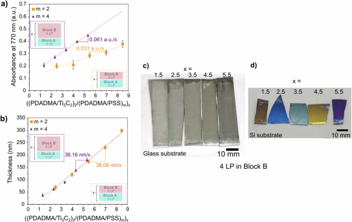
a UV–Vis absorbance and (b) thickness of [(PDADMA/Ti3C2Tz)2/(PDADMA/PSS)m]x heterostructures with 0.5 M NaCl in block B. Digital photographs of [(PDADMA/Ti3C2Tz)2/(PDADMA/PSS)4]x with 0.5 M NaCl in block B heterostructures at various x/LbL cycles on (c) glass and (d) Si substrates. Digital photographs of [(PDADMA/Ti3C2Tz)2/(PDADMA/PSS)2]x with 0.5 M NaCl heterostructures (the case of m = 2) are provided in Fig. 2c, d.
As before, QCM was employed to determine the areal mass composition of each block in the heterostructure. For the case of m = 4, the average areal mass deposited per blocks A and B were 9.91 μg/cm2 and 4.54 μg/cm2, respectively (or 69 wt % for block A and 31 wt % for block B), resulting in a MXene composition of 62.1 wt% of MXene in this heterostructure. This also corresponds to approximately 28 MXene nanosheets stacked for every block A section. These measured values were also summarized in Supplementary Table 2. In comparison, the case of m = 2 (described in the previous section) contained 54.9 wt% MXene. The higher mass fraction of MXene in the case of m = 4 explains the heterostructures’ higher absorbance growth rate and darker appearance. The areal mass, however, did not double upon increasing m from two to four (3.00 vs 4.54 μg/cm2, respectively). The difference can be attributed to possible partial removal of the previous layers by stripping, as previously discussed. Also, for lower numbers of layer pairs, LbL growth is patchy, resulting in incomplete surface charge reversal11,41,42,43. We speculate that two layer pairs of block B results in patchy growth that might prevent the robust adhesion and adsorption of subsequent MXene layers. In comparison, four LPs of block A resulted in more robust MXene layer adsorption, leading to a larger MXene content.
The heterostructures exhibited a range of colors as more layers were added, as seen in Figs. 2c–f and 3c, d. Within the digital photographs, a difference in color richness was observed depending on the substrate for heterostructures of the same composition and layer pair number. As the overall thickness of the heterostructures was relatively thin, incident light transmitted through the films and interacted with the substrates. With the silicon substrate being more reflective than the glass substrate (and PET substrate in Supplementary Fig. 3), the heterostructures on the silicon substrate appeared to have a richer color. The influence of the substrate was removed through filtering/baselining in subsequent UV–Vis measurements. Across all three heterostructures, we observe that as the number of layer pairs increases the reflectance peak decreases (Fig. 4). This layer-pair-dependent change in reflectance illustrates the opportunity to create a wide variety of optical coatings (e.g., mirrors, notch filters, induced transmission filters, or gradient-index lenses) with the same materials simply by varying layer thicknesses during the LbL assembly process. The drop in reflectance is due to an estimated increase in absorptance, as the relationship between reflectance (R), transmittance (T), and absorptance (A) is
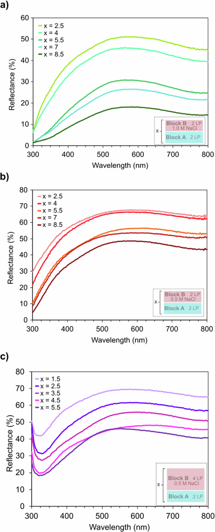
a [(PDADMA/Ti3C2Tz)2/(PDADMA/PSS)2]x with 1.0 M NaCl in block B, (b) [(PDADMA/Ti3C2Tz)2/(PDADMA/PSS)2]x with 0.5 M NaCl in block B, and (c) [(PDADMA/Ti3C2Tz)2/(PDADMA/PSS)4]x with 0.5 M NaCl in block B heterostructures.
It is important to note that the absorbance values mentioned within the previous sections (and in Supplementary Fig. 1) do not carry the same definition as A in Eq. (1). Those absorbance values were the output of the UV–vis spectrophotometer, which relied on the presumed relationship between absorbance and transmittance used within the Beer–Lambert law44,45,46. While literature often uses these terms interchangeably and both denoted by the variable “A”, they are not the same due to limitations made around the assumptions required by the Beer–Lambert law47. The absorbance value from the Beer–Lambert law assumes light is not scattered, as in homogenous medium (e.g. solutions). However, we know our heterostructures must scatter light, as confirmed by the presence of structural color. Yet, we permitted the use of said absorbance in previous sections as it was utilized to quantify heterostructure growth; but when directly discussing the optical characteristics of the heterostructure, this value is no longer appropriate. To further avoid any issues in optical spectra analysis, the reflectance values in Fig. 4 were taken with a different UV–vis spectrophotometer (Hitachi U-4100 UV–Vis–NIR) that was capable of directly measuring reflectance as described in Eq. (1). This way the reflectance discussed throughout this section was independent of the absorbance values above.
The reflectance plots in Fig. 4 show broad peaks centered at wavelengths dependent on the heterostructure composition and block thicknesses. Within the set of heterostructures that contained 0.5 M NaCl in 2 LP thick block B, Fig. 4b, this peak shifted from being centered around ~580 nm to ~605 nm then back down to ~570 nm, as the layer pairs increased. This peak shifting is also present in the set of heterostructures that contained 0.5 M NaCl in 4 LP thick block B, Fig. 4c; the peak center shifted from ~575 nm to a max of ~642 nm before dropping down to ~550 nm. Unlike the other two compositions, the heterostructures containing 1.0 M NaCl in 2 LP thick block B, Fig. 4a, showed minimal peak shifting, generally staying centered around ~565–575 nm. This film set also had lower reflectance values compared to the others.
Notably, the reflectance spectra of all three heterostructures featured one broad peak within the selected wavelength range. This differs from films that yield structured color solely due to thin film interference, which normally exhibits a reflectance spectrum containing a periodic sinusoidal pattern36,48. The presence of a sinusoidal pattern signature denotes that such films can be thought of as gradient-index homogenous blocks, rather than distinct multilayered heterostructures. Here, the lack of a sinusoidal pattern in the reflectance spectra for our heterostructures, along with the variant refractive indices/dielectric constants of the two blocks, suggests that the structural coloration in [(PDADMA/Ti3C2Tz)2/(PDADMA/PSS)m]x heterostructures is similar to a distributed Bragg reflector or quarter-wave optical stack21,23,49.
If the observed color changes with viewing angle, then structural coloration is considered angle-dependent (such as with the iridescence of a soap bubble or the feathers of a pigeon)50. If the observed color remains the same with changes in the viewing angle, then the structural coloration is considered angle-independent51. Because the reflected color is related to the peak reflectance wavelength of an object’s reflectance spectrum, angle-dependent optical characterization can be used to determine whether the structural color is angle agnostic. In the case of angle-independent structural coloration, the peak in reflectance should occur at the same wavelength at different incident light angles. Conversely, if the reflectance peak shifts for different incident angles of light, then structural coloration is angle-dependent, and the object exhibits iridescence. By visual inspection, all the heterostructures exhibited structural color independent of angle except for [(PDADMA/Ti3C2Tz)2/(PDADMA/PSS)2]8.5 with 0.5 M NaCl in block B. Supplementary Video 1 shows an example of angle-dependent structural colors arising from this heterostructure. To compare, UV–vis reflectance spectra were collected at multiple incident angles of light for each heterostructure. The selected angles were 0°, 15°, and 30° (based on machine limitations) and were defined as the angle between the sample normal and beam of incident light. Two of the three samples represented in Fig. 5, [(PDADMA/Ti3C2Tz)2/(PDADMA/PSS)2]8.5 with 1.0 M NaCl in block B (Fig. 5 center), and [(PDADMA/Ti3C2Tz)2/(PDADMA/PSS)4]4.5 with 0.5 M NaCl in block B (Fig. 5 right), were selected as representatives for their heterostructure set. [(PDADMA/Ti3C2Tz)2/(PDADMA/PSS)2]8.5 with 0.5 M NaCl in block B (Fig. 5 left), which exhibited angle-dependent structural coloration, was selected to represent its heterostructure set.

Bar chart displaying the reflectance peak wavelength for 0°, 15°, and 30° (from sample normal) incident angles of light for [(PDADMA/Ti3C2Tz)2/(PDADMA/PSS)2]8.5 with 0.5 M NaCl in block B (left), [(PDADMA/Ti3C2Tz)2/(PDADMA/PSS)2]8.5 with 1.0 M NaCl in block B (center), and [(PDADMA/Ti3C2Tz)2/(PDADMA/PSS)4]4.5 with 0.5 M NaCl in block B (right) heterostructures.
Examination of Fig. 5 confirms our visual observations. The reflectance peak wavelengths of the [(PDADMA/Ti3C2Tz)2/(PDADMA/PSS)4]x with 0.5 M NaCl in block B heterostructure and the [(PDADMA/Ti3C2Tz)2/(PDADMA/PSS)2]x with 1.0 M NaCl in block B heterostructure remain nearly the same despite the incident angle of light (around 571 nm where x = 8.5 and 573 nm where x = 4.5, respectively), consistent with angle-independent structural coloration. In contrast, the heterostructure of [(PDADMA/Ti3C2Tz)2/(PDADMA/PSS)2]8.5 with 0.5 M NaCl in block B exhibited a reflectance peak wavelength that changed with the different incident light angles. Specifically, at 0°, 15°, and 30°, the reflectance peaks occurred at 563 nm, 582 nm, and 561 nm, respectively; this observation is consistent with angle-dependent structural coloration. As determined by the previously discussed QCM data, this specific heterostructure composition contains the highest amount of PDADMA/PSS.
Within the literature, PDADMA/PSS LbL films were determined to show angle-dependent structural coloration36. Also in literature, and previously mentioned, Ti3C2Tz has been used under films comprised of SiO2 that show angle-dependent structural coloration to make them angle-independent structurally colored27. We speculate that the [(PDADMA/Ti3C2Tz)2/(PDADMA/PSS)2]8.5 with 0.5 M NaCl in block B heterostructure does not contain enough MXene in the structure to offset the angle-dependent structural coloration nature of the PDADMA/PSS block, causing this to be the only composition to show angle-dependency instead of angle-independency in the structural coloration. Another explanation for the differing structural color angle dependency could be due to some form of interlayer roughness between the two blocks in the heterostructures. Texture can influence optical response52,53,54,55. Revisiting the AFM images of the heterostructures (Fig. 1c), we observe nano-wrinkles in the surface, caused by overlapping MXene nanosheets. The images (specifically Fig. 1c right) also show how the wrinkles are preserved after the deposition of block B, displaying how the interlayer roughness is carried throughout the heterostructure. These wrinkles may cause a diffuse reflection where light is scattered in multiple directions, which could induce consistent structural color independent of viewing angle52,56. Because the [(PDADMA/Ti3C2Tz)2/(PDADMA/PSS)2]x with 1.0 M NaCl in block B and [(PDADMA/Ti3C2Tz)2/(PDADMA/PSS)4]x with 0.5 M NaCl in block B heterostructure systems contain more MXene nanosheets and these nanosheets are the cause of the wrinkles on the interlayer surfaces, this could also explain why all block pairs within these heterostructure systems exhibit angle-independent structural color.
To further validate the observed structural coloration (both angle-independent and angle-dependent), the CIE 1931 chromaticity coordinates (x, y, Y) were calculated and plotted. In Fig. 6, a photo of each film set on an Si substrate is displayed with the corresponding CIE color space plot. Within this plot the luminosity (the Y coordinate) value is not represented; however, the values are summarized in Supplementary Table 1. We observe heterostructures made with 0.5 M NaCl in 2 LP block B (Fig. 6a) go from a deep orange (x = 2.5) to blue (x = 4), to yellow (x = 5.5), to another hue of orange (x = 7), and then back to another hue of blue (x = 8.5), as x grows. Heterostructures made with 1.0 M NaCl in 2 LP block B (Fig. 6b) go from gold (x = 2.5) to orange (x = 4), to blue (x = 5.5), to turquoise (x = 7), and to green (x = 8.5). The 0.5 M NaCl in 4 LP block B containing heterostructures (Fig. 6c) first appear brown at x = 1.5, then become blue (x = 2.5), pale teal-green (x = 3.5), yellow (x = 4.5), and then deep purple (x = 5.5).

CIE 1931 color space plots of structural color of heterostructures. Colors of heterostructures with x as indicated plotted in CIE 1931 color space next to photo of films on Si wafer; (a) [(PDADMA/Ti3C2Tz)2/(PDADMA/PSS)2]x with 0.5 M NaCl in block B, (b) [(PDADMA/Ti3C2Tz)2/(PDADMA/PSS)2]x with 1.0 M NaCl in block B, and (c) [(PDADMA/Ti3C2Tz)2/(PDADMA/PSS)4]x with 0.5 M NaCl in block B heterostructures.
The 1.0 M NaCl in 2 LP block B-containing heterostructures noticeably follow a pattern that follows the Newton series of colors. This series characteristically describes a cycling sequence of ordered color groups that is often seen in nature and within thin films48,57,58. In this case, as x increases, we move clockwise around the CIE color space (starting with the gold color of x = 2.5; as displayed by the white spiral in Fig. 6b). This phenomenon may also be evident within the 0.5 M NaCl in 2 LP block B containing heterostructures with the pattern going twice clockwise around the CIE color space (reference the white spiral in Fig. 6a); however, due to the large jumps across the color space with the selected LP intervals, further investigation is needed to confirm. Similarly, heterostructures with 0.5 M NaCl in 4 LP block B also follow the same twice-around clockwise pattern (see white spiral in Fig. 6c).
The optical properties of a material define how light contorts, or refracts, when passing through a medium or material. The complex refractive index, (widetilde{n}), is expressed by a real part, n, and an imaginary part, ik to obtain:
In the case of the polyelectrolyte blocks of the heterostructures, the wavelength dependency of refractive index can be modeled using the Cauchy dispersion model59,60:
The Cauchy model assumes there is negligible influence of the extinction coefficient, k. With this assumption, only the real part, n, of the complex refractive index remains and the Cauchy model is the most abecedarian formula that relates refractive index to wavelength with the help of the parameter constants, A, B, and C, that are determined based on equation fitting around known values of n and λ.
However, unlike the polyelectrolytes in block B and dielectric nanomaterials in previously reported optical filters21,23,26,61, the Cauchy dispersion model cannot be used to describe the optical properties of the Ti3C2Tz MXene/PDADMA blocks. When derived via spectroscopic ellipsometry analysis, Fig. 7a, there is a significant contribution from the extinction coefficient throughout visible and infrared wavelengths. There is also variation within the real part of the refractive index as well due to Kramers–Kronig relations. As such, these layer materials must be modeled with a Drude–Lorentz model62,63,64:
Where ε1 is the real component and ε2 is the imaginary component of a materials’ dielectric constant. These components are defined by the permittivity of free space (ε∞), frequency of light (ω), plasma frequency (ωp), and damping constant (γ).

a MXene-rich block A and (b) polymer-rich block B refractive indices measured using spectroscopic ellipsometry. c Experimental (cyan line) and OpenFilters-generated (magenta line) reflectance spectra of the [(PDADMA/Ti3C2Tz)2/(PDADMA/PSS)4]2.5 heterostructure with 0.5 M NaCl in block B.
The n and k of the two blocks were entered into OpenFilters software and used to generate a modeled reflectance spectrum for a selected number of block pairs. QCM data was used to choose initial thickness inputs for the blocks. The first modeled spectrum (See Supplementary Fig. 2) underestimated the reflectance spectrum for a [(PDADMA/Ti3C2Tz)2/(PDADMA/PSS)4]2.5 heterostructure with 0.5 M NaCl in block B. Despite being off by a factor of 10, the general shape of the generated spectrum matched the experimental reflectance spectrum for this heterostructure (found in Fig. 4c).
Because n and k of the PDADMA/MXene block were calculated from a sample only containing block A, the loss of loosely adhered MXene sheets through LbL stripping that occurs in the heterostructure is not optically accounted for. So, the n and k of block A were multiplied by a constant with a value between 0 and 1 to adjust the model-generated reflectance spectrum. Various values were fitted and a multiplier value of 0.19 produced a reflectance spectrum most similar to the experimentally measured reflectance. It should be noted that a constant multiplier was also applied to n and k of block B, but then removed as it did not contribute to matching the experimental data. This is likely due to the use of a Cauchy model (i.e., normal dispersion only) to block B (seen in Fig. 7b), as discussed in the previous section, compared to the Drude–Lorentz model for block A representing anomalous dispersion characteristics. An improved derivation of block A optical properties is likely possible upon appending variable angle spectroscopic ellipsometry data with transmission intensity data and will be the focus of future work.
The OpenFilters software is equipped with a feature that allows the user to input optical targets and then consequently adjust the block thicknesses to achieve or approximate the targets. Through using this feature with reflectance targets that matched experimental reflectance data at wavelengths of 800 nm, 500 nm, and 390 nm, and manual manipulation of the thickness input, the model reflectance spectrum in Fig. 7c (magenta line) was created. The model block thicknesses are 20 nm for block A and 31 nm for block B.
In Fig. 7c, both the experimental and the modeled spectra for the [(PDADMA/Ti3C2Tz)2/(PDADMA/PSS)4]2.5 heterostructure with 0.5 M NaCl in block B are plotted showing the visible wavelength regime, about 300 nm to 800 nm. Despite artificially adjusting the parameters to generate the modeled spectrum, it remains slightly off from the experimental. From 300 to 315 nm, the model underestimates the reflectance. From 315 nm to 770 nm the model then overestimates the reflectance, however at 500 nm the two values differ by less than 1%. While the [(PDADMA/Ti3C2Tz)2/(PDADMA/PSS)4]2.5 model does not show the local reflectance minimum at 331 nm, when additional blocks were added to the model to represent the [(PDADMA/Ti3C2Tz)2/(PDADMA/PSS)4]3.5 heterostructure with 0.5 M NaCl in block B (see Supplementary Fig. 2), the experimental reflectance minimum is reflected in the model. However, this generated spectrum is shifted to the right (red shift) when compared to the experimental data (Fig. 4c).
Within this study, we made three different LbL heterostructures compromised of two main alternating blocks. The first block, MXene-rich A, contained 2 LPs of PDADMA/Ti3C2Tz, while the second block, polymer-rich B, contained either: 2 LPs of PDADMA/PSS assembled with 0.5 M NaCl, 2 LPs of PDADMA/PSS assembled with 1.0 M NaCl, or 4 LPs of PDADMA/PSS assembled with 0.5 M NaCl. By examining the growth behavior of each heterostructure, we demonstrated that the thicknesses of the blocks and the MXene content could be controlled at the nanometer scale. The color of each heterostructure, as represented by the reflectance spectra, changed with heterostructure type and thickness. The majority of the heterostructures exhibited angle-independent structural coloration, while only one showed angle-dependent structural coloration, possibly due to internal roughness between the blocks.
These results allow for a glimpse into deeper understanding of how varying the spatial placement and concentration of MXene nanosheets within a LbL heterostructure in terms of growth and optical properties. Due to the heterostructures showing structural coloration, our future research will use inverse design to tailor-make MXene LbL heterostructures of specific thicknesses to yield a predicted response. This future effort could lead to the creation of dielectric mirrors and other optical filters with a variety of designated optical targets.
Methods
Materials
Poly(diallylmethylammonium) chloride (MW = 200,000 to 350,000 g/mol, 20 wt% in water) and sodium chloride (NaCl) were purchased from Sigma-Aldrich. Polystyrene sulfonate sodium (MW = 500,000 g/mol) and linear polyethylenimine (LPEI, MW = 25,000 g/mol) were acquired from Polysciences Inc. Citric acid (CA, MW = 192.13 g/mol), isopropyl alcohol (IPA, 99%), acetone ( > 99.55%), and slide glass (75 × 25 × 1 mm) were obtained from VWR. Ti/Au quartz crystal substrates (5 MHz) were attained from Inficon. Si wafers were purchased from University Wafer. 18.2 MΩ cm (Milli-Q) water was accumulated from a Milli-Q integral water purification system for ultrapure water.
MAX phase synthesis
Nanolayered, hexagonal transition-metal carbides/nitrides, or MAX phases, are the precursors of MXenes. These materials follow the formula Mn+1AXn, where n = 1-3, M is a transition metal, A is an A-group element, and X is carbon or nitrogen65,66. MAX phase powders were fabricated by pressureless sintering, as in previous reports38. Ti, Al, and TiC powders were combined using a molar ratio of Ti:Al:C = 3:1.2:1.95 to create the Ti3AlC2 MAX phase. The powders were mixed in a jar rolling mill (300 rpm, 12 h) with 35 mm diameter ZrO2. Ensuing milling, powders were sintered in alumina crucibles in a 50 mm alumina tube furnace at a rate of 10 °C/min to 1510 °C under constant argon flow (4 h). Powders were cooled to room temperature, then ground into particles 20–45 μm in size by mortar and pestle.
MXene synthesis
MAX phase powders were processed into MXene colloidal dispersions using the procedures described in previous reports38. In brief, to form HF in situ for etching, 3.3 g LiF was added to 50 mL of 6 M HCl (constantly stirred) in a polypropylene beaker. Before use, holes were drilled into the top of the beaker to prevent pressure build-up and help regulate heat from the exothermic reaction. Following dissolution, the solution was heated to 40 °C. 5 g of Ti3AlC2 at a rate of 1 g/min then set to etch (45 h). The mixture was brought to pH 6, by removing excess etchant in a centrifugal washing progress (9000 rpm, 20 min). Dimethylsulfoxide (16.67 mL per gram of starting MAX phase) was added to the Ti3C2Tz clay, then stirred (20 h). A centrifugal solvent exchange method with deionized water (5000 rpm, 4 h) for three cycles was employed to rid the clay of excess intercalants. Bath sonication (1 h) was used to delaminate the clay. The resulting dispersion was centrifuged (3500 rpm, 1 h) and the supernatant was collected. The concentration of the final mono- and few-layer Ti3C2Tz nanosheet dispersion was deduced by vacuum filtration of a known dispersion volume. MXene characterization of this synthesis method is reported in Supplementary Fig. 4.
Layer-by-layer assembly
Once the MXene dispersion was synthesized, the concentration was diluted to 1 mg/mL. The MXene solution acted as the anion within the first distinct LbL block (block A) of the heterostructure; the polycation was PDADMA. To improve oxidative stability throughout the LbL assembly process, 1 mg/mL of CA was added as an antioxidant to all block A ion solutions and washes38. The second cation/anion combination within the heterostructure (block B), again used PDADMA as a polycation, while the anion in this block was PSS. Polyelectrolyte solutions and Milli-Q washes within block B contained NaCl (0.5 M or 1.0 M).
Glass and Si wafer substrates were bath sonicated in isopropyl alcohol for 15 min, then washed with water and acetone. Once dried, the substrates were plasma treated for 5 min. Plasma treatment allows for the substrate to become negatively charged and hydrophilic. Ti/Au quartz crystal substrates followed a slightly different preparation protocol. First, they were plasma treated for 10 min, then cleaned using a basic piranha solution (5:1:1 Milli-Q water: ammonium hydroxide: hydrogen peroxide, at 75 °C). Afterwards, quartz crystals were plasma treated for 10 min.
Subsequently, substrates were immersed in LPEI solution (1 mg/mL, pH 4, 15 min) to create a base layer. The substrate was then consecutively submerged in three washes of Milli-Q water and 1 mg/mL CA (1 min each). After the washing, the substrate was dried with compressed air to prevent contamination and aggregation. Following this, samples were placed into the MXene dispersion (15 min), washed (Milli-Q water and CA, 1 min) thrice, and dried. This created a single-layer pair (LP). To continue assembling block A of the heterostructure, the substrates were placed into PDADMA solution as before, washed, dried, then submerged once again in the MXene dispersion. This alternating was continued until the desired number of LPs was reached within block A.
Block B was created on top of block A by following the same assembly procedures for PSS and block B PDADMA, apart from the washes containing a selected concentration (0.5 M or 1.0 M) of NaCl, instead of CA. Once the necessary number of LPs in block B were created, additional block A LPs were assembled, once again repeating the same procedures until the heterostructure was completed. Samples were stored at room temperature under vacuum to remove any water in between layers and protect from MXene oxidation.
Thin film characterization
To characterize the growth profiles of the films, spectrophotometry and profilometry were used. The film thickness in relation to layer pair number was measured using a profilometer (KLA Tencor D-500). The profilometer was also used to determine the root-mean-square (RMS) roughness (Rq). Quartz crystal microbalance (QCM; Inficon MAXTEK) was used to confirm film growth by recording the frequency change for every LP then using the Sauerbrey equation to obtain the mass deposited. Surveying the films assembled on the glass slides with a UV–Vis–NIR spectrophotometer (Shimadzu SolidSpec-3700 UV–vis–NIR, Hitachi U-4100 UV–Vis-NIR), absorbance and reflectance were measured. Along with confirming growth, measuring absorbance also allowed for a glimpse into the optical response of the heterostructures. The reflectance spectra also quantified optical performance.
Film sets were mapped within the CIE 1931 color space. To create the chromaticity plot, a representative pixel within digital images of the films was selected and translated into CIE (x, y, Y) coordinates, then plotted in the color space.
Spectroscopic ellipsometry (Nanofilm EP3 ellipsometer) was utilized to collect optical dispersion data to derive the optical constants of the two blocks (A and B) on single-side polished Si wafers. The Si wafers had a native oxide of ~2 nm in thickness. Analysis using CompleteEASE v6.55 (J.A. Woollam) was performed to gather refractive indices and extinction coefficients from the optical dispersion data. OpenFilters software was used to create a multilayer one-dimensional model of the heterostructures using the derived optical constants.
Scanning electron microscopy (SEM; JEOL JSM-7500F) was also used to examine the morphologies of the different heterostructures. Si substrates of the completed films were scored and placed into liquid nitrogen for 1 min, then removed and fractured along the score line. This process allows for a clean break for the best view of the heterostructure’s cross section. Before mounting the sample, it was sputter coated until a thickness of 5 nm was achieved to reduce film charging.
Transmission electron microscopy (TEM; Thermo Fisher Titan Themis Z 300) was used to view the cross-sectional morphology of the heterostructure. TEM samples were prepared using a Tescan LYRA-3 Model GMH dual-beam focused ion beam (FIB) system. The ion (Ga+) beam operated at 30 kV with a beam current ranging from 12 nA down to 70 pA. The TEM lamella preparation consists of 4 steps: 1. Pt deposition of a protection layer on the area of interest; 2. Milling symmetrical trenches around the lamella and U cut; 3. Lift out using the nanomanipulator and attached to TEM grid; 4. Final thinning and cleaning. TEM observation was conducted in an aberration-corrected transmission electron microscope at 300 kV. The composition of the sample was analyzed using a Super-X EDS in the STEM mode. The camera length in the STEM mode was 115 mm.
An atomic force microscope (AFM; Bruker Dimension Icon AFM) inspected the surface morphologies of the heterostructures. Both block A and B were examined as the terminating block, leaving the MXene layer on top in block A and the PSS layer on top in block B. Each film was created on a Si substrate.

Responses