Demonstration of 4-quadrant analog in-memory matrix multiplication in a single modulation

Introduction
An AIMC core performs analog MVMs between a stationary weight matrix encoded in it and a digital vector applied at its input. Weight matrix elements are encoded as the analog conductance values of resistive memory devices placed along the rows and columns of a crossbar array. Input vector elements are applied as voltages along the rows, resulting in a current flow at columns which, when integrated and converted to digital by an analog-to-digital converter (ADC), provides the result of the MVM. Different resistive memory device technologies can be used for AIMC1,2,3, such as phase-change memory (PCM)4,5,6, resistive random-access memory (RRAM)7,8,9, magnetoresistive random-access memory10,11 and ferroelectric field-effect transistors12. Recent advancements in multicore AIMC chips reveal that analog computations can accurately conduct MVMs necessary for the forward pass in deep neural networks (DNNs), promising significant improvements in energy efficiency compared to traditional digital accelerators4,5,7,8,9.
Despite the exciting opportunities for efficient and fast computation, AIMC also introduces a set of unique challenges that must be addressed to realize its full potential. One critical point is to minimize the MVM latency, which directly impacts both the energy efficiency and throughput of the core. Indeed, even if AIMC avoids weight data transfers and allows it to perform a fully parallel MVM computation, it will not be competitive with respect to digital accelerators if the MVM latency is too long due to slow input/output data conversion and processing. In fact, most of the recent AIMC chips based on resistive memory devices report a 256 × 256 MVM latency higher than 1 μs, which is too slow6,7,13,14. Usually, when a bit-parallel approach is used to apply inputs by modulating the read-voltage pulse duration according to the input magnitude (e.g., a 7-bit unsigned input can be applied with a duration of 0–127 ns using a 1 GHz clock), multiple read phases are needed to process the different signs of inputs and/or weights which slows down the computation4,5. In the bit-serial approach proposed in ref. 7, each input bit is applied one at a time with a single pulse, therefore the number of applied pulses corresponds to the number of input bits (e.g., a 7-bit unsigned input is applied with 7 1-bit pulses). Signed inputs and weights are processed simultaneously by applying input voltage pulses with opposite polarities to adjacent rows, but two read phases are needed for inputs greater than 4 bits to reduce the number of cycles for charge integration on the output capacitor, leading to a latency of >10 μs for an 8-bit input 256 × 256 MVM. Using two’s complement representation for inputs and weights allows the analog processing using a single voltage polarity13, but it requires exact bitwise analog computation, which limits the number of rows that can be accumulated in parallel (sometimes as low as 414) to maintain sufficient signal margin8. Therefore, multiple phases, each activating a different set of rows, are needed to perform large MVMs8. An approach that allows the performance of fully parallel MVM computation in a single read phase could significantly improve the latency over previous schemes, which is the subject of this paper.
A circuit design for executing a 256 × 256 4-quadrant MVM in a single modulation cycle was proposed by Khaddam-Aljameh et al.15. However, the documented MVM outcomes relied solely on a four-phase reading scheme. This method processes each quadrant individually with a single voltage polarity, which reduces the chip’s maximum throughput and energy efficiency by approximately fourfold4. In order to implement single-phase MVMs, a different calibration procedure than that presented in ref. 15 is needed to account for additional circuit and device nonidealities, which we address in this paper. By implementing this new analog/digital calibration procedure on the IBM HERMES Project Chip4, we experimentally demonstrate a 4-quadrant MVM in a single modulation that achieves sufficient precision for DNN inference and similarity search applications. We thoroughly quantify the achievable MVM accuracy compared with the four-phase scheme and show near software-equivalent application results executed on up to six cores of the chip.
Results
Single-phase analog matrix multiplication
To perform an MVM on a core of the IBM HERMES Project Chip, the magnitude of each 8-bit signed-magnitude integer (INT8) input element is converted into a 7-bit pulse duration ranging from 0 to 127 ns generated via a 1 GHz clock. The input modulator applies the pulse-width-modulated (PWM) read-voltage pulses to the PCM array, the output of which is digitized by an array of 256 time-based current ADCs. The PCM array comprises 256 × 256 unit cells, each comprising four PCM devices. Positive weights are represented by the combined conductance value of two PCM devices (G+), and negative weights by the other two PCMs of the unit cell (G−). Figure 1a illustrates the conventional implementation of an MVM in four phases demonstrated in previous works4,15. Positive and negative inputs are applied individually to the two source lines (SLs) connected to positive and negative weights in four modulation cycles using a single voltage polarity. The positive and negative components of the ADC output are subtracted digitally in the local digital processing unit (LDPU). The MVM latency in this mode is approximately four times the modulation time (4TPWM).

a In-memory MVM in four phases. Inputs of positive and negative polarity are applied individually to weights of positive and negative polarity using a single voltage polarity (V−) in four modulation cycles 4TPWM. b In-memory MVM in a single phase. Inputs of positive and negative polarity are applied simultaneously to weights of positive and negative polarity with voltages of opposite polarity (V+, V−) in one modulation cycle TPWM. c Implementation of the single-phase in-memory MVM on the IBM HERMES Project Chip. The procedure is shown for a single BL of an AIMC core of the chip. ΔV refers to the voltage drop on the SL with respect to Vcm, e.g., ΔV = V+,− − Vcm. In the abbreviations for the SL connections shown on the left, the first letter refers to the SL polarity, and the second to the polarity of the read voltage applied at the bottom electrode of the PCM devices. For example, PN means connecting SLP to V−. When the SL input is >0, the PN and NP switches are activated, and when it is <0, PP and NN are activated.
Figure 1b illustrates the single-phase MVM read procedure, enabling parallel reading of all unit cells of the PCM array in one modulation cycle TPWM. Initially, all selection transistors are activated to engage the entire array, and the bit-lines (BLs) are pulled to the common-mode voltage, Vcm. Then, based on the input vector signs, the different SLs are connected to either
when current is to be added, or
to subtract current, by applying a negative voltage drop at the top electrode with respect to the bottom electrode of the PCM device. This allows all four combinations of ± inputs and ± weights to be taken into account in a single modulation without the need for negative voltages. The SL connections for all four combinations of products between a positive or negative weight and a positive or negative input are shown in Fig. 1c. When the input is positive, SLP is connected to V− and SLN to V+, and vice-versa when the input is negative.
The currents from the positive and negative BLs, BLP,i, and BLN,i, are then summed in the analog domain and arrive to the read voltage regulator of the ADC, as shown in Fig. 1c. The regulator is connected to a Schmitt trigger that captures the current polarity information in the signal D. The mirrored BL current is then fed into the second part of the ADC, which is the current-controlled oscillator (CCO), to generate a proportional time-encoded signal15. This time-encoded current information is then integrated in two 12-bit counters. Depending on the signal D, positive and negative counter outputs ADCP and ADCN are incremented at a rate proportional to the BL current. This process is repeated for the varying BL currents of all 127 input timesteps, whereby the currents of the different timesteps are integrated in the respective counter depending on their polarity. Thereafter, ADCP and ADCN are subtracted in the LDPU. The subtracted ADC output then undergoes an affine transformation and optional rectified linear unit (ReLU) operation in 16-bit floating-point (FP16) arithmetic. The output is finally converted to INT8 format, ready to be transferred to other cores.
There are several challenges in achieving a high MVM accuracy with the above scheme. First, the conductance of PCM devices read at low voltages depends on the voltage polarity16. The conductance of the PCM devices of a single core of the chip measured in positive and negative polarity using Vread ≃ 0.2 V is shown in Fig. 2a. On average, the high conductance (SET) states show no voltage polarity dependence. The intermediate states, however, show a polarity dependent conductance, the conductance being higher in the negative than in the positive polarity. The ratio between the conductance in the positive polarity and in the negative polarity increases with increasing conductance values. This behavior is explained by the presence of varying Schottky barriers at the electrode-amorphous and amorphous-crystalline interfaces of the PCM device, which have state-dependent contact areas (see Fig. 2b, c)16. Moreover, a significant inter-device variability in the conductance polarity dependence is also observed. This leads to additional errors when performing MVMs with signed inputs that are crucial to mitigate through on-chip calibration. Second, in addition to PCM device nonidealities, manufacturing mismatches lead to gain and linearity variations between positive and negative ADC circuits, which also need to be compensated through calibration15. Third, accurately detecting the current polarity with the Schmitt trigger in the presence of noise, especially when the current magnitude is small, can be problematic and lead to signal D being set to the wrong polarity. In the following section, we describe a robust analog/digital calibration procedure, fully implemented on-chip, that mitigates those three challenges for obtaining accurate MVM results with the single-phase read scheme.
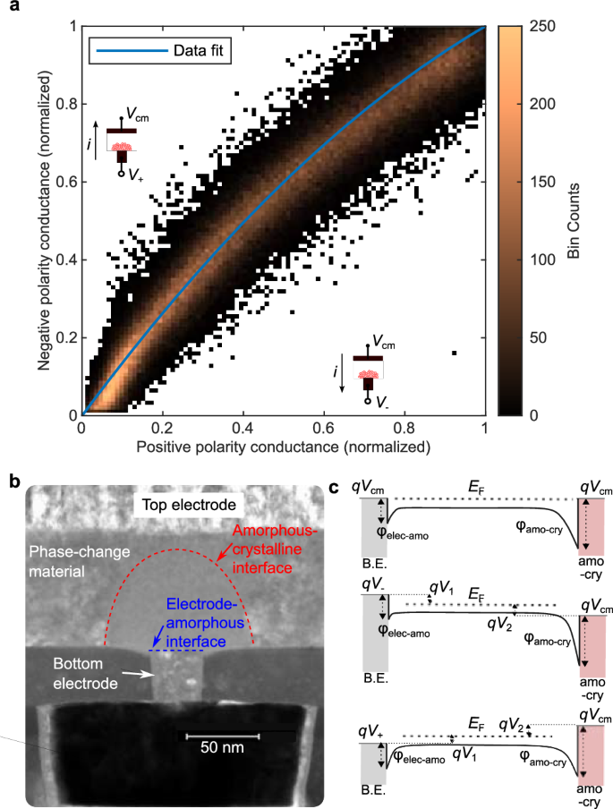
a Conductance measured in negative voltage polarity as a function of conductance measured in positive voltage polarity at Vread ≃0.2 V for 130 k PCM devices of an AIMC core. The blue line is a guide to the eye that shows the average trend. In order to compare the polarity dependence of devices that have different SET conductance on the same graph, the conductance of each device is normalized by the SET conductance of that device for each polarity. The mean SET conductance of all devices is approximately 20 μS. b Low-angle annular darkfield scanning transmission electron microscope image of a fully RESET PCM device showing a substantially large amorphous region that fully blocks the bottom electrode. Electrode-amorphous and amorphous-crystalline interfaces are highlighted. c Band diagrams of the PCM device at equilibrium, under positive and negative polarity bias. Only the valence band is shown because the Ge2Sb2Te5 material is a p-type semiconductor in the amorphous phase. Schottky barriers for holes appear at both interfaces, with the barrier of the amorphous-crystalline interface greater than that of the electrode-amorphous interface16. When a positive bias is applied at the top electrode with respect to the bottom electrode, the back-to-back diode configuration entails the amorphous-crystalline interface being reverse-biased and the electrode-amorphous interface forward-biased. This effect reverses when the polarity is negative. Thus, larger current flows when the dominating diode is forward-biased, which is the amorphous-crystalline interface. This occurs for the negative polarity of the applied bias, i.e., when Vcm is applied at the top electrode and V+ at the bottom electrode.
Implementation
The control inputs per ADC that can be tuned in order to calibrate it are underlined in Fig. 1c. The main current-mirror gains αP,i and αN,i set the static ADC gain. The nonlinearity is reduced by increasing the gains βP,i and βN,i, which control the feed-forward delay compensation circuit of the CCO. Finally, any read-voltage variation-related offset is compensated using ({tilde{v}}_{{{rm{read}}},{{rm{i}}}}), which is varied by selecting a different tap from a resistor ladder. In addition to the analog ADC calibration, a per-ADC tunable digital affine correction can be done in the LDPU to equalize any remaining difference. A complete step-by-step pseudo-code of the calibration procedure can be found in Supplementary Fig. 1.
The calibration procedure starts by programming all devices of the core to the low conductance (RESET) state. The transfer curves (ADC count as a function of the input current) of the 256 ADCs prior to calibration are shown in Fig. 3a for both ADCP and ADCN. The transfer curves are measured by gradually activating one SL after the other. First, we tune ({tilde{v}}_{{{rm{read}}},{{rm{i}}}}) to minimize the offset current. The offset current comes from parasitic currents flowing between the BLs due to the crossbar topology, when the various read voltage regulators settle on different Vread values due to mismatches, and therefore strongly depends on V+, V−, and Vcm supply values (here chosen as 0.6, 0.2, and 0.4 V, respectively)15. This tuning is done by setting half of the SL inputs to a positive value and the other half to an equal in magnitude negative one and then measuring the ADCP and ADCN outputs. The same procedure is performed again by inverting the polarity of the inputs. The four offsets retrieved are then summed with their respective sign. This procedure ensures that the resulting total offset is independent of the array conductance values. Depending on the total offset, ({tilde{v}}_{{{rm{read}}},{{rm{i}}}}) is either decreased or increased until the total resulting current converges to zero. This calibration ensures that summing two MVMs with inputs of equal magnitude but opposing polarity results in a total current close to zero. Therefore, besides compensating for individual offsets of ADCP and ADCN, it also corrects the average conductance polarity dependence of the PCM devices by shifting the BL potential towards V+ or V−.
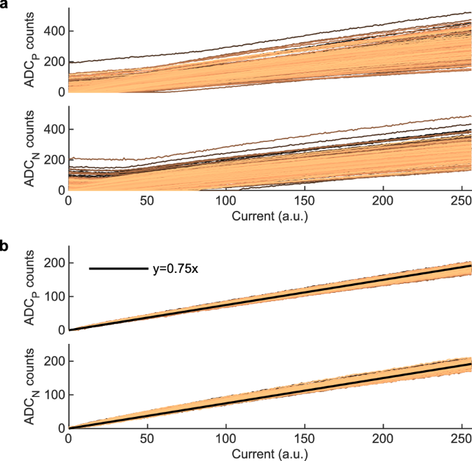
a Positive (ADCP) and negative (ADCN) transfer curves of the 256 ADCs prior to calibration. b ADC transfer curves after calibration. The transfer curves are measured with all devices of the core programmed to the RESET state, by gradually activating one SL after the other, starting from 0 up to 256 SLs.
Subsequently, we correct for the gain and linearity variations between positive and negative ADC outputs by adjusting the ADC gain parameters αP,i and αN,i, and then the feed-forward gains βP,i and βN,i. In both cases, this is done by adjusting the parameter such that the distance between the measured transfer curve and a linear characteristic with a reference gain of 0.75 ADC count per active SL is minimized. Parameters for ADCP and ADCN are adjusted independently in a sequential manner. The transfer curves of the 256 ADCs after this calibration are shown in Fig. 3b. For both ADCP and ADCN, the offsets are close to 0, the gains are equalized, and the transfer curves are linear.
After this initial analog calibration stage, the weights provided by the application are programmed as the conductance values of PCM devices using the Max SET Fill algorithm17. A weight is written by programming the two PCM devices that correspond to the weight polarity. Devices of the opposite polarity are RESET to near-zero conductance. Depending on whether the weight fits on one or two devices, we program the first device to either RESET or SET state, respectively, and run an iterative program-read-verify algorithm on the second device (see Methods)17. Note that the chip also allows the use of only a single device per weight polarity, which achieves higher memory density at the expense of lower MVM accuracy4. For reading the PCM devices during programming, we apply positive inputs to positive weights and negative inputs to negative weights by default, such that only ADCP is used during readout. In the specific case where the application would require only positive inputs to be applied to the core, for example, if the core receives inputs from a ReLU activation function, we apply positive inputs to both positive and negative weights during programming. In this way, the conductance polarity dependence can be compensated during programming by using either ADCP or ADCN for readout depending on the weight polarity. A comparison of the MVM accuracy resulting from those two readout methods will be shown in Section “MVM accuracy result”.
After the programming phase, it is important to recalibrate ({tilde{v}}_{{{rm{read}}},{{rm{i}}}}) with the same procedure described previously. This recalibration is necessary due to the polarity dependence of the conductance. As shown in Fig. 4, after programming uniformly distributed weights (within [−1, 1] range) in the core, the currents measured for ADCN are higher, on average, than the currents for ADCP. Therefore, when subtracting ADCN from ADCP, a large total offset remains. This is because the conductance of the intermediate states is higher in the negative than in the positive polarity (see Fig. 2). The initial calibration was done on a fully RESET array which does not show such polarity dependence, therefore recalibration of ({tilde{v}}_{{{rm{read}}},{{rm{i}}}}) post-programming is necessary. As shown in Fig. 4, this recalibration step is effective in bringing the total offset closer to 0.
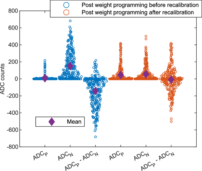
ADC values are measured when setting half of the SL inputs to a positive value and the other half to an equal in magnitude negative one after uniformly distributed weights within [−1, 1] range have been programmed in the core. The expected distribution of ADCP − ADCN values should be centered around zero, which is effectively achieved after recalibration.
To tackle the third key challenge, namely, the difficulty in detecting the current polarity with the Schmitt trigger in the presence of noise when the current magnitude is small, we add a bias current to shift the zero point to a positive current value. This is done by programming bias weights in the last SLs of the array and applying bias inputs to them for every MVM. This bias is then subtracted by digital post-processing in the LDPU. The number of SLs to be used for biasing depends on the application (distribution of weights and inputs). In general, the bias utilized is a trade-off between the size of the linear regions for negative and positive outputs, as well as how accurately the bias can be corrected digitally. For example, a small bias will lead to lower correction errors (because it is less noisy), but the negative linear region will be narrow. On the other hand, a large bias will produce more noise and hence more errors after digital correction, and a narrower positive linear region. In our experiments, we found that using 16 of the 256 available SLs for bias achieves a good tradeoff.
Finally, we perform a per-ADC tunable digital affine correction in the LDPU to correct any remaining mismatch as well as to subtract the bias. For this, we perform a number of MVMs with input vectors of values with the same statistics as those in the application. These can be either randomly generated or taken from a training set. After performing the MVMs and obtaining raw results from the ADCs, a first-degree polynomial fitting is used to fit these raw results to the exact results computed in floating-point. This way, per-ADC scale and offset correction factors that compensate for gain mismatches and bias, respectively, are obtained. The digital correction factors are calibrated only once after the weights have been programmed; they are not recalibrated while running the application.
MVM accuracy results
First, we characterize the accuracy of MVMs performed with sparse uniform distributions of weights and inputs. About 30% of the weights and 10% of the input values are equal to zero, and the remaining are uniformly distributed. The reference results for the 4-quadrant MVMs realized with the four-phase operation as performed in previous works4 (one phase per input/weight sign combination with inputs supplied only to V−) are shown in Fig. 5a. The normalized MVM error from this experiment is 11.9%. The results for the 4-quadrant MVMs realized with the single-phase operation described in Section “Implementation” are shown in Fig. 5b. The observed nonlinear region comes from a plateau region around the point where the MVM current is zero, due to the distortion resulting from the imprecise detection of the current polarity with the Schmitt trigger when the current magnitude is small. Thanks to the bias shifting technique, the nonlinear MVM response is shifted to negative values, while the zero point and positive outputs show a linear behavior. Although the negative outputs are less accurate, there are many applications for which only the positive outputs are needed, which will be presented in Sections “ReLU-based neural network” and “Similarity search”. The normalized MVM error from the positive outputs of this experiment is 13.6%. Finally, we present outcomes for 2-quadrant MVMs with exclusively positive inputs (see Fig. 5c). In these instances, we adjust for the conductance dependence on polarity during the programming phase, as detailed in Section “Implementation”. Here, the normalized MVM error from the positive outputs goes down to 11.8%, similar to the reference four-phase measurements.
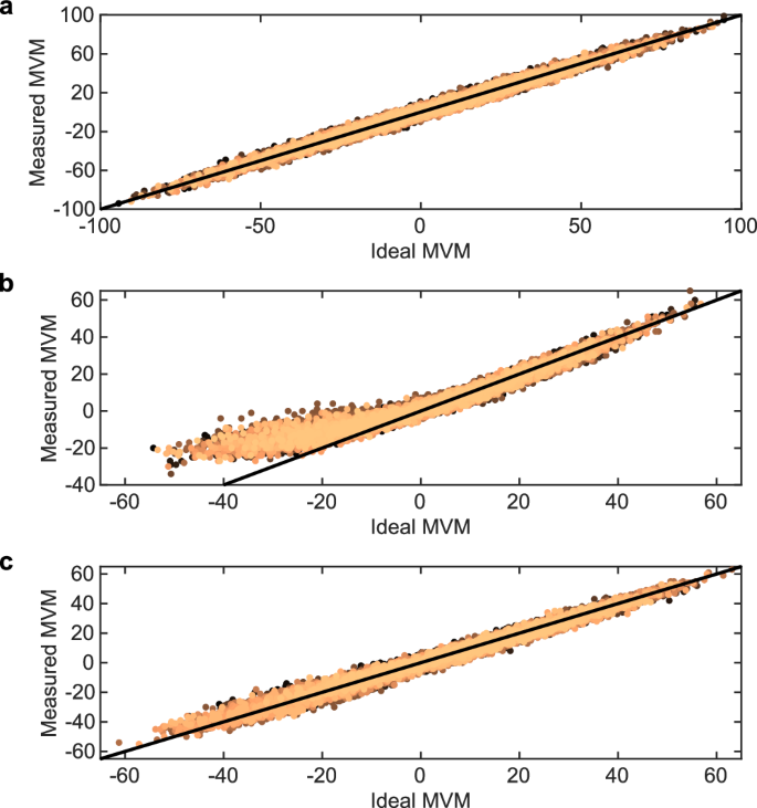
a 4-quadrant MVM results using the conventional four-phase reading scheme. b 4-quadrant MVM results using the single-phase reading scheme. c 2-quadrant MVM results (positive-only inputs) using the single-phase reading scheme. The black line in the plots is a y = x guide to the eye.
ReLU-based neural networks
As a first application, we consider a convolutional neural network (CNN) for the MNIST handwritten digits recognition benchmark. We implemented a CNN consisting of 3 convolution layers and 1 dense layer on one core of the chip, as shown in Fig. 6a, b. The network is trained by injecting Gaussian noise with a standard deviation of 0.1 at the output of each layer to improve the robustness to hardware noise18, along with L2 regularization (λ = 10−4) and dropout with rate of 0.5 before the dense layer (see Methods). For the inference experiments, input data preparation and pooling are done in software, the rest is performed on-chip. Because a ReLU activation function is used at the output of every convolution layer, the weight matrix is programmed to be optimized for 2-quadrant MVMs with positive-only inputs (see Fig. 5c).
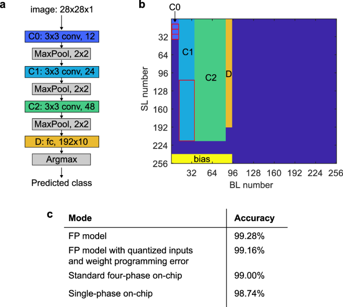
a Network used for MNIST handwritten digit recognition. b Implementation of the network on one core of the chip. The weights of the first and second layers are replicated 4 and 2 times, respectively, as indicated by the red borders. The inputs to those layers are also replicated the same number of times. This is done to increase the input current to the ADC and average the weight programming noise, which improves the signal-to-noise ratio and leads to higher accuracy. The last 16 SLs of the core are reserved for the bias weights (see “Implementation”). c Accuracy obtained from the on-chip experiments with four-phase and single-phase reading schemes compared with the accuracy of the same model run in software (FP model).
Figure 6c presents the achieved results and compares them to the software FP32 models and the standard four-phase implementation. The FP32 model, which yields an accuracy of 99.28% on the test set, is taken as the starting benchmark. When accounting for the weight programming errors and quantized inputs, the FP32 model accuracy is 99.16%. When it comes to the IBM HERMES Project Chip operational modes, the standard four-phase mode achieves an accuracy of 99.00%. The developed single-phase mode resulted in an accuracy of 98.74%, which is only 0.54% lower than the FP32 model accuracy.
Similarity search
As a second application, we consider performing an in-memory similarity search in the context of few-shot continual learning (FSCL) tasks. FSCL requires a learner to incrementally learn new classes from very few training examples, without forgetting the previously learned classes. An architectural solution for FSCL that combines a stationary DNN with a dynamically evolving explicit memory (EM) was introduced in ref. 19. The EM, implemented with AIMC cores, dynamically updates its content at each learning session by storing distinct class-wise embeddings from new unseen examples.
Using pretrained stationary DNNs identical to ref. 20, we perform the inference stage of FSCL by implementing the EM unit using multiple cores of the IBM HERMES Project Chip. The inference stage is composed of a continual learning phase of novel classes from five support examples per class, and a query evaluation phase in which we evaluate the accuracy over a batch of query examples. In our implementation of the continual learning phase, the forward pass of the DNN and computing of the key vectors are fully implemented in off-chip software. The chip is reprogrammed with the newly learned key vectors (one per class) at each session. The key vector elements are bipolarized to +1/−1 values to be programmed on G+/G− PCM devices, respectively. Then, for the query evaluation phase, we quantize the DNN output vector elements to 8-bit and apply them to the SLs of the AIMC cores to execute single-phase MVMs. This performs an in-memory similarity search between the query vector and the key vectors. The class corresponding to the maximum element of the resulting output vector from the chip is then taken as the predicted class. Because this maximum element is usually much greater than the output elements of the other classes, bias weights are not needed in this application.
We first present FSCL inference results on the CIFAR-100 and miniImageNet datasets, using a single core of the chip to implement the EM (see Fig. 7a). All accuracies obtained with the chip using the single-phase reading scheme are less than 1% below the software accuracies computed in FP32. The fact that the EM uses bipolar vectors, which avoids any inaccuracy coming from state-dependent conductance polarity dependence, as well as the high separation of the predicted class output from the rest, contributes to achieving such software-equivalent accuracies. Finally, to show that more than a single core of the chip can be calibrated to properly execute the single-phase reading scheme, we implemented the EM for FSCL on the Omniglot dataset on six cores (see Fig. 7b). Here as well, all accuracies obtained with the chip are less than 1% below the software accuracies.
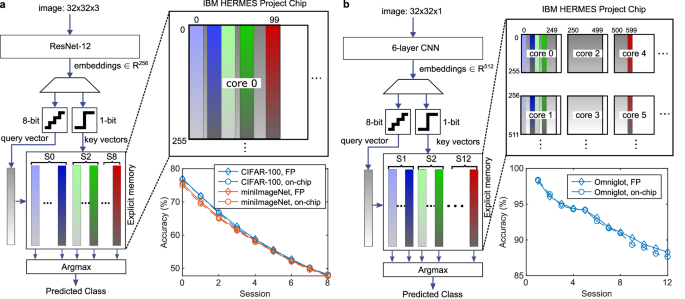
a Accuracy obtained from the on-chip experiments with the single-phase reading scheme compared with the software accuracy (FP) for the inference stage of FSCL tasks on the CIFAR-100 and miniImageNet datasets. The dataset contains natural images of 100 classes in total, which are divided into a first session (S0) containing 60 classes with 200 training and 100 query examples per class, and eight subsequent sessions (S1–S8) with 5 novel classes introduced in each session containing 5 support examples and 100 query examples per class. The learned key vectors occupy 256 SLs and 60 BLs (classes) on the array in S0, evolving to 100 BLs (classes) in the last S8. b Accuracy obtained from the on-chip experiments with the single-phase reading scheme compared with the software accuracy (FP) for the inference stage of FSCL tasks on the Omniglot dataset. The dataset contains handwritten figures of 1623 characters from 50 alphabets. For FSCL evaluation we use 600 character classes from the test set organized into 12 sessions. Each session contains 50 classes, and each class consists of 5 support examples and 15 query examples. The learned key vectors are 512 dimensional and mapped across a pair of cores. The lower 256 dimensions of a key vector are mapped to all 256 SLs in one core, and the higher 256 dimensions are mapped to 256 SLs in a second core along the corresponding BLs. The 250 class vectors until the 5th session can be mapped to 250 BLs in one pair of cores (core 0, core 1). Similarly, sessions 6th to 10th can be mapped to core 2, core 3. Finally, the 11th and 12th sessions’ key vectors are mapped to 100 BLs across core 4 and core 5.
Discussion
In summary, we presented the experimental realization of a 4-quadrant MVM with AIMC in a single modulation by simultaneously applying positive and negative voltages to the resistive memory devices. It enables the fastest way to perform large MVMs with AIMC, limited only by the modulation duration and a one-time SL pre-charge. The latency achieved by the IBM HERMES Project Chip for a 256 × 256 MVM executed in this mode is 133 ns, leading to a peak MVM throughput-per-area of 1.55 TOPS/mm2 and energy efficiency of 9.76 TOPS/W, approximately 4× higher than with the conventional four-phase mode4. Even if the single-phase MVM accuracy is lower and only positive outputs can be utilized, it can be used to accelerate MVMs in certain applications that are robust to imprecision and still achieve software-equivalent performance. However, to achieve this performance, a rather elaborate analog/digital calibration procedure had to be performed, and recalibration after weight programming was necessary to mitigate the conductance polarity dependence of PCM devices. After recalibration, it was found that the conductance polarity dependence increased the MVM error by 1.8% compared to a positive-only input MVM. Further device and material engineering will be needed to reduce this effect and its device-to-device variability in PCM devices that are asymmetric. In case geometrically symmetric devices are used instead, such as RRAM, such a polarity dependence might not be prominent, and recalibration would not be necessary. However, irrespective of the memory technology, we expect that the proposed calibration procedure to mitigate ADC mismatches and the addition of a bias current will be beneficial in most designs that simultaneously apply positive and negative voltages on the memory devices to perform MVMs. At the circuit level, to avoid the burden of recalibrating every time new weights are programmed on PCM and other asymmetric devices, alternate single-phase read schemes that operate only with a single voltage polarity deserve further investigation.
Methods
Chip and experimental platform
Our experimental results are demonstrated on chips from 300 mm wafers fabricated with PCM inserted in a 14 nm back-end-of-line (BEOL) at IBM Research at Albany NanoTech. The BEOL fabrication, including PCM mushroom cell formation, is done on top of the foundry-sourced front-end wafers. The PCM mushroom cell is comprised of a ring heater for the bottom electrode and a doped Ge2Sb2Te5 and top electrode film stack, which is subtractively patterned to form the mushroom top.
The experimental platform is built around a single chip packaged in a 1525-pin ball grid array (BGA). Through controlled collapse chip connection (C4), the chip can be mounted onto an interposer printed circuit board, which is placed on a socket for testing on a dedicated test board. For every core, 72 dedicated C4 pads provide analog and digital supply voltages in addition to a small number of pads used to implement a serial communication interface to control the core.
The chip is interfaced with a hardware platform comprising one field-programmable gate array (FPGA) module and a baseboard. The base board provides the chip socket, chip cooling, multiple power supplies per power domain as well as the voltage and current reference sources for the chip. A Trenz TE0808-04 module with Xilinx Zynq UltraScale+ FPGA is used to implement overall system control and data management as well as the interface with the chip. The experimental platform is operated through Ethernet from a host computer, and a Python environment is used to coordinate the experiments. Supplementary Figure 2 shows a picture of the chip and of the experimental setup.
Weight programming
Iterative programming involving a sequence of program-and-verify steps is then used to program the selected devices to the desired conductance values21. After each programming pulse, a verification step is performed, and the value of the unit-cell conductance programmed in the preceding iteration is read. The read is performed by applying long PWM pulses of 0.2 V amplitude with 512 ns width and 256 ns precharge time to ensure a reliable read of the small individual conductance values by the ADCs. The programming current applied to the PCM device in the subsequent iteration is adapted according to the value of the error between the target level and the read value of the unit-cell conductance. The unit-cell conductance is obtained by reading the conductance value of each PCM device individually, and computing (left({g}_{1}^{+}+{g}_{2}^{+}right)-left({g}_{1}^{-}+{g}_{2}^{-}right)). The programming pulses are square pulses of 125 ns width and amplitude varying between 125 μA and 700 μA. The programming sequence ends when the error between the target conductance and the programmed conductance of the unit cell is smaller than a margin of 5 ADC counts or when the maximum number of iterations (30) has been reached.
CNN training on MNIST benchmark
The CNN was constructed with the Keras Sequential API. It consists of 3 convolution layers of kernel size 3 × 3 with 12, 24, and 48 filters, respectively, each followed by a ReLU activation and a 2 × 2 max pooling layer (see Fig. 6a). After the convolution layers, the output is flattened and sent to a dense layer of size 192 × 10 using softmax activation for classification. L2 regularization with λ = 10−4 is used on all layers. During training, Gaussian noise with a standard deviation of 0.1 is injected at the outputs of the 3 convolution layers, and the dense layer before the activation layer, and dropout with a rate of 0.5 is used before the dense layer. The training is performed with the Adam optimizer and categorical cross-entropy loss as an objective for 100 epochs with a batch size of 128, using 10% of the training data as validation.
Few-shot continual learning DNN pretraining
For CIFAR-100 and miniImageNet datasets, we use a Resnet-12 architecture as the feature extractor. It consists of four residual blocks with block dimensions [64, 160, 320, 640], each containing three convolutional layers with batchnorm and ReLU activation. After the final global average pooling, we get output activations with dimension df = 640. This is passed through a fully connected layer that projects the Resnet outputs to embeddings of dimensionality d = 256. The feature extractor is first pretrained under a supervised classification setting using the base session training images by appending another fully connected layer, giving its weight matrix shape (d, 60). This pretraining step improved the overall accuracy of the base session by up to 15%. Next, the meta-learning is performed by drawing a new 60-way 5-shot problem in every iteration from the base session training images and updating the model based on ten queries per way. The model is trained for 70,000 iterations using a stochastic gradient descent (SGD) with momentum 0.9 and weight decay 5 × 10⁻⁴. The learning rate is initially set to 0.01 and reduced by 10× at iterations 30,000 and 60,000.
For the Omniglot dataset, we use a feature extractor that involves 4 convolutional layers with 128 channels and 2 × 2 maxpooling at the end of the second and fourth layer, followed by a fully connected layer that resizes the flattened embedding to df = 512 before feeding to another fully connected layer that outputs the embeddings of dimensionality d = 512. During the meta-learning, the model is trained for 70,000 iterations with an Adam optimizer with a learning rate of 10−4. A data augmentation scheme is used during meta-learning whereby images are rotated and shifted in each of x– and y-axis with standard deviations 0.26 and 2.5, respectively.


Responses