Enhanced performance and functionality in spintronic sensors

Introduction
Magnetic sensors are an integral part of our daily lives. They are found in a variety of applications ranging from mobile devices and household appliances to automotive, aerospace, and industrial settings1. In data centers, the hard disk drive continues to be a fundamental component. The read elements used in these drives led to innovations in magnetic field sensing by continuously pushing the limits of technology, reaching ever-smaller dimensions while maintaining the highest performance. Yet, the applications of magnetic sensors have expanded beyond information storage. More specifically, such sensors are now being explored for precision healthcare2,3,4,5, food safety and environmental monitoring6,7, advanced information and communication technologies8, robotics and prosthetic control9,10, wearables and augmented reality11,12,13, and car electrification and autonomous driving14,15.
Spintronic sensors, specifically those based on giant and tunnel magnetoresistance (GMR and TMR, respectively), provide suitable solutions for magnetic field detection. They deliver high sensitivity and spatial resolution15,16, alongside large output signals and signal-to-noise ratios17. These MR devices are also characterized by low power consumption and compact sizes, the latter achieved through well-established fabrication methods. Furthermore, their compatibility with standard integrated-circuit patterning techniques enables monolithic integration with complementary metal-oxide-semiconductor10 and mechanically flexible substrates18, fitting the next-generation of ultra-compact commercial electronics. The roadmap for MR sensors outlined development milestones and highlighted several unresolved technological issues in key applications19.
In this perspective, we address future developments of spintronic sensors and their impact in current research areas and potential new applications. With a focus on GMR and TMR technologies, we first propose novel strategies to enhance their overall performance by addressing four open challenges. We then introduce possible ways to create a new class of adaptable sensors with on-demand tunable properties and added functionality. Such advancements will require innovative approaches at all levels, including the incorporation of novel material systems, new device designs and the use of alternative fabrication methods.
In the end, this vision to enhance and expand operational limits of MR sensors aims to impact current applications and pave the way for new uses. These could include (but are not limited to) adaptable biomedical platforms, remote motion detection, spatially resolved field mapping, or new instrumentation for quantum sensing. Such advances will profit from the versatility of MR technology, while helping to maintain its competitiveness within the landscape of magnetic field sensing.
Background
GMR and TMR sensors are solid-state magnetic devices composed of thin-film multilayers. Their working principles rely on spin-dependent charge transport2,20,21, resulting in a resistance value that depends on the magnitude18,22 and direction13,23 of an external magnetic field. In its simplest form, one of the basic building block of these MR multilayered systems is a ferromagnet/spacer/ferromagnet trilayer [Fig. 1a—①/②/③], where each layer is only a few nanometers thick. Depending on the type of sensor, this trilayer will combine ferromagnets (FM) (Fe, Co, Ni, and their alloys) for sensing and fixed layers, with either a conductive (e.g., Cu for GMR) or insulating (e.g., AlOx, MgO for TMR) spacer. The resistance changes with the field are determined by the relative orientation between the magnetization of both FMs [Fig. 1b]. To establish a reference orientation for measurements, one of these FMs is adjacent to an antiferromagnet (AFM) [Fig. 1a—③/④]. This arrangement sets a unidirectional magnetic reference built into the multilayered stacking, achieved by interfacial exchange bias24.

a Schematic design of the multilayered thin-film that acts as the building block for in-plane magnetized MR sensors. The labels indicate layers that are key to the sensor operation and have a dominating role in setting its final performance. These are ①—sensing layer, designed so that the magnetization ((overrightarrow{M})) follows the external magnetic field; ②—spacer, that sets the maximum MR value; ③—reference layer, where (overrightarrow{M}) is fixed by interaction with an adjacent ④ antiferromagnet. b Representative R(H) output curve. Each major feature of R(H) can, as a first approximation, be directly linked to one of the key layers highlighted in (a). The final sensor performance is a result of the entire multilayer characteristics. The arrows indicate the relative orientation of (overrightarrow{M}) in ① and ③.
These spintronic devices can serve as highly sensitive magnetic field sensors, given that their electrical resistance can change by factors much larger than those possible with single-layer and simple magnetic materials. Figure 1b shows an output curve representation of an in-plane magnetized MR sensor. It depicts the change in resistance as a function of the field from a minimum (RP) to a maximum (RAP) value, coinciding with the relative orientation of the FM layers’ magnetization ((overrightarrow{M})), either parallel or antiparallel. The magnetoresitance ratio is defined as MR(%) = RAP − RP/RP × 100. This is a key parameter for high sensitivity, and therefore, the combination of materials’ type and thicknesses are optimized to achieve its highest values16. For this, thin film growth with precise thickness control is required.
The transition between RP and RAP is engineered to be linear, reversible, and hysteresis-free. This is achieved by manipulating the magnetic anisotropy energy of the sensing layer [Fig. 1a ①] to reverse the magnetization through a quasi-coherent rotation16. The field sensitivity is then given by MR/ΔHlinear (%/mT), where ΔH is the interval where R(H) is linear. In advanced sensing multilayers at room temperature, GMR spin valve systems typically show MR signals of around 6–10%13,17, while TMR MgO-based tunnel junctions reach up to around 200%5,23,25. These values are obtained for quite complex stackings that go beyond the FM/spacer/FM trilayer structure by having: (i) buffers with low resistivity, controlled crystallography and roughness for a proper growth of the spacer, the AFM, and the synthetic (SAF) antiferromagnets; (ii) magnetic references with exchange-biased SAFs; (iii) composite sensing layers for hysteresis-free behavior and low magnetic noise; and (iv) capping (hard) layers for protection against oxidation and patterning. For TMR sensors, achieving a high MR ratio by optimizing the barrier thickness also affects other major operation parameters, namely the resistance-area product4, noise levels26,27,and barrier breakdown limit28, all of which impact the final device design and performance, especially the signal output.
Finally, the control of the noise level is critical in setting the limit of detection29. The field detection level is calculated from SV/(MR/ΔH) (T/(sqrt{Hz})), where SV is the voltage noise. For GMR and TMR sensors, SV includes contributions from 1/f noise, random telegraph noise, and thermal noise22. For TMR, shot noise is also present30. Different strategies to define ΔH, minimize noise, and maximize MR, are available based on materials nano-engineering25,31,32, device geometry16,17, or both15,33. All these points are elaborated and discussed in section “Open challenges”.
Landscape of magnetic sensing technologies
The family of magnetic sensors is vast and encompasses distinct operation and detection principles beyond GMR or TMR2,22. We highlight several sensor families due to their competitive performance and briefly note some key characteristics enabling a link to the challenges and perspectives discussed in sections “Open challenges” and “Adaptable features and functionality”, while giving targets for continuous improvements of MR technology. Therefore, this subsection is not designed to review thoroughly other technologies and their advantages or limitations. For that, the mentioned references should be consulted.
Within the magnetic thin-film-based sensors, those based on the Hall effect stand out due to the simplicity of their multilayered system and fabrication processes when compared to GMR or TMR34,35. This makes them a cost-effective choice and quite widespread in commercial applications. A recent review34 showcases the advances in planar Hall sensors, and discusses new strategies to improve their limit of detection, with best values of few (pT/sqrt{Hz}) below 10 Hz. A subset of this family and a quite recent development in this research area36,37,38 explores the combination of detection via anomalous Hall effect with the characteristics of spin-orbit torque (SOT) and spin Hall magnetoresistance in ferromagnetic/heavy-metal bilayers35,36,39. This sensor concept resorts to spin-polarized currents to control the magnetization orientation in the ferromagnet and, with that, achieve a linear R(H) 37. These SOT-enabled Hall sensors have been used for three-dimensional field measurements36,39, and for offset control of the R(H) linear window relative to zero field40. One main bottleneck is the low output signals, for which possible solutions in combination with TMR structures have been proposed35,38, but not yet demonstrated. Nevertheless, inspired by the practical implementation of SOT in spintronics memories1,41, potential opportunities in field sensors could include the development of hybrid SOT/MR devices (section “Adaptable features and functionality”).
Superconducting quantum interference devices (SQUIDs) yield high sensitivity and spatial resolution, reaching the fT range at low frequencies. Recent advances include novel materials42, improvements in sample-to-sensor positioning43, and downscaling for improved resolution42. However, cryogenic cooling is necessary during measurements to preserve the superconducting state, which hampers miniaturization and portability. Nitrogen-vacancy (NV) defect centers in diamond have been pushing the limits in magnetic field detection, enabling high-resolution imaging at the nanoscale44,45. Reported values range from tens of (mu T/sqrt{Hz}) for single NV to (pT/sqrt{Hz}) for NV ensembles depending on the detection protocols46. NV centers have been used to probe the nanoscale magnetic behavior and textures, thus giving new fundamental insights into condensed matter physics44, and aided wafer-level analysis45. Key challenges for this technology are scaling up measurement areas and ensuring optimal resolution by minimizing NV center to sample distance. Optically-pumped magnetometers (OPMs) are another emergent yet very competitive and sensitive tool with reported limits of detection of ~14 pT47. Their specifications are closer to SQUIDs’ but with a more compact size, making them a good candidate to become a leading sensing technology. The sensor circuitry includes a vapor cell and requires many optical components, and therefore, a major breakthrough was the demonstration of a portable tool working at ambient conditions, showing 16 fT/cm/√Hz in a gradiometer configuration to detect brain and heart signals48. Even though these systems have top performance in field detection and spatial resolution, their hardware complexity and operation mode can complicate the design of compact solutions. These challenges hinder efforts to make them smaller, integrated, and portable, areas where GMR and TMR have significant advantages. Nevertheless, substantial progress is underway to overcome these limitations. Therefore, new strategies to ensure the competitiveness of spintronics-based sensing technology, as those outlined in sections “Open challenges” and “Adaptable features and functionality”, can be crucial for future developments.
Open challenges
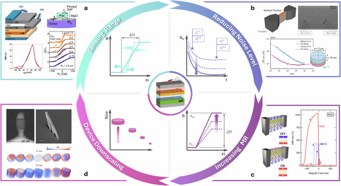
The development of spintronic sensors with enhanced performance involves the optimization of major figures of merit. In this section, we will briefly address the state-of-the-art and share our views on future developments to improve sensitivity by controlling the linear sensing range (ΔH), minimizing the noise level (SV), and maximizing MR values. All these characteristics may vary depending on device’s dimensions.
Linearization and sensing range
The output signal in MR sensors, whether measured in voltage or resistance, is designed to be a linear function of the external field [Fig. 2a]. Depending on the requirements for the final application, a linear R(H) curve is established, characterized by a nearly absent coercive field within ΔH. GMR and TMR sensor’s output is commonly linearized by patterning the elements into elongated shapes16,17. Their dimensions and geometry define ΔH due to a dominating effect of the shape anisotropy. Therefore, decreasing the element’s width leads to increasing aspect-ratio (i.e., length/width), and consequently larger ΔH, which has a negative impact in the sensitivity. In GMR, sensing layers with a configuration close to a compensated SAF allowed partial recovery of such losses49. In TMR, linearization strategies that do not rely on elongated shapes were successful by using circular elements with exchange-biased sensing layer31,32. The smallest elements with diameter of 120 nm, displayed field sensitivity of 3.7%/mT and ΔH close to ±15 mT31. The main advantage was the control of ΔH by changing the pinning strength of the FM/AFM interface. However, multiple annealing steps were necessary to set a crossed magnetization configuration at zero field, resulting in low thermal resilience32. An overall increase in the noise level was also present due to higher resistances and magnetic disorder as a consequence of the interfacial bias16.
Conceptual view (center) of the challenges discussed in section “Open challenges” and their impact on the sensors’ performance by engineering the characteristics of the materials and devices. Our vision is built on demonstrations of: (a) Linear sensing range can be tuned using—left—oblique ion deposition of the FM layers with ΔH of ±50 mT (ref. 54 under CC-BY with no modifications) or —right—by changing the reference layer dimensions in a vortex configuration with ΔH≤ ±5 mT (Reproduced with permission from33 ©IOP Publishing); (b) Reducing the noise level by having—top—multiple repetitions of the multilayer stack in a vertically packed arrangement to reduce the device’s resistance and thus ({S}_{V}^{Th}) (ref. 17 under CC-BY with no modifications) or—bottom—by having a vortex configuration at the sensing layer that shows overall lower SV (ref. 15 reproduced with permission from SNCSC); (c) Increasing magnetoresistance values can be achieved with—rigth—Mg-Al-O barriers showing up to 1000% at low temperature (ref. 62 under CC-BY with no modifications) or—left—by having the entire stack composed of 2D van der Waals materials (Reprinted with permission from ref. 69. Copyright (2018) by the American Physical Society); (d) Device downscaling to ultra-small sizes of few nanometers—top-left—(Reprinted from ref. 82 with the permission of AIP Publishing) using advanced patterning techniques such as—top right—3D nano-printing (ref. 71 under CC-BY with no modifications) or by exploring core-shell arrangements—bottom (Reprinted with permission from ref. 86 ©2024 by the American Physical Society).
While numerous research works focus on decreasing ΔH as required for challenging biomedical applications that need high field sensitivity4, a promising outlook in electrical vehicles profits from having larger ΔH of up to hundreds of mT14,15,50. For this, an out-of-plane magnetized reference can be used together with a sensing layer that is also out-of-plane magnetized14,50, or is at the onset of superparamagnetism51. Although, the latter has typically lower thermal resilience and higher noise levels.
Alternatively, topologically protected structures such as vortices can also deliver wide ΔH. Added benefits include lower magnetic noise (see section “Open challenges”)15, and negligible dipolar coupling between neighboring elements, suitable for high-density packing52. To establish a vortex state at the sensing layer, the soft FM thickness, and the lateral dimensions are carefully adjusted. With that, competing shapes and intrinsic anisotropies induce a flux closure magnetization configuration, which is very robust against external fields. The vortex core position, however, can gradually change with the external magnetic field15. A R(H) with a linear operation window can thus be defined with ΔH of ± 25 mT reported for GMR15 and up to ±5 mT for TMR33. Further ΔH tunability down to ±1 mT was proposed by Endo et al. by varying the diameter of the reference layer, analogous to the use of shape anisotropy [Fig. 2a]33. At the nanoscale, such a vortex configuration has been used for neuromorphic computing53, but was not yet leveraged for sensing.
Tailoring the intrinsic magnetic anisotropy adds another knob for in-stack defined and adjustable ΔH. Willing et al. employed oblique ion deposition to set crossed in-plane anisotropies in both the sensing and the reference layers54. The magnetization direction was defined by combining deposition angles and layer thicknesses, leading to a ΔH ± 40 mT with an TMR of ~20% [Fig. 2a].
Artificial defect engineering, such as ion irradiation55 or patterning of nanovoids56, offers other possibilities for tailored magnetic anisotropy. Teixeira et al. reported a 30% decrease in the out-of-plane anisotropy after Ar+ irradiation at fluences of 1014cm−2, leading to an in-plane canting of the magnetization57. The authors attributed this result to a decrease in saturation magnetization and increased interfacial mixing, which reduced the perpendicular magnetic anisotropy. In another example, Co/Pd multilayers suffered a reduction in the coercive field from 600 mT to 50 mT when the diameter of the patterned non-magnetic inclusions increased from 180 nm to 200 nm, decreasing its wall-to-wall distance to 20 nm58. Thus, edge defects and roughness at nanometer scale act as sites of reduced anisotropy, promoting the nucleation of reversed magnetic domains and resulting in smaller coercive fields. This strategy, however, also increases resistivity due to confined current paths, which in spintronic sensors will mostly likely lead to lower MR values. Nevertheless, these two methods provide options, at wafer level, to design neighboring elements enclosing different sensitive axes, overcoming current limitations of elongated shapes and discrete assembly.
Reducing the noise level and increasing magnetoresistance
The minimum value of the magnetic field that a spintronic sensor can detect is set by the smallest measurable voltage output and its noise level (SV). Reducing noise in MR sensors has been a paramount task [Fig. 2b]22,30. Various methods have been tested for this purpose, each inherently linked to the targeted frequency of detection. If the latter is below 1 kHz, it often falls within the 1/f noise-dominated regime (({S}_{V}^{,1/f}))26. This contribution has both electric and magnetic components and depends on the element size. Random telegraph noise (RTN, ({S}_{V}^{,RTN})) also appears at low frequencies and is usually associated with magnetic inhomogeneities and magnetization fluctuations in the sensing layer26,59. At higher frequencies, the white noise background is reached, which includes the thermal noise (({S}_{V}^{,Th})) determined by the device resistance, and (also) shot noise (({S}_{V}^{,shot})) for TMR sensors30.
Incorporating vortex configurations in GMR delivered lower noise levels by a factor of 7 (at 10 Hz) when compared to elliptical structures [Fig. 2b]15. Irreproducible magnetic reversal in the sensing layer of elements with shape anisotropy leads to increased magnetic noise, and by employing a flux-closed configuration, a reproducible vortex-core motion in response to external fields is achieved, thereby mitigating this source of noise. As for TMR, increasing the sensing layer thickness (>10 nm) and using amorphous-like materials enhances its soft magnetic properties. The result is a reduced hysteresis in R(H) and thus reduced voltage noise, meeting the criteria for lower ({S}_{V}^{1/f}) and ({S}_{V}^{,RTN})4,25,60. For a sensing layer composed of 20 nm thick CoFeBTa, a reported SV of 40 ({rm{nV}}/sqrt{{rm{Hz}}}) at 10 Hz resulted in a detection level of (2.2,{rm{nT}}/sqrt{{rm{Hz}}}). This performance was 7x better than that achieved with fcc NiFe25. However, using thick layers requires thorough control of both crystallography and anisotropy, in addition to the ability to either fabricate very tall pillars with well-defined vertical walls, or having a precise end point control for etching, placing pressure on patterning methods (see subsection below). Additionally, doping the MgO barrier with Al is another promising possibility for reducing ({S}_{V}^{1/f}) associated with charge trapping within the barrier and at its interfaces61. The lattice constant in Mg-Al-O tunnel barriers can be tuned by changing the Mg-Al composition ratio, leading to an improved lattice matching interface with the TMR bcc ferromagnetic electrodes62. In fact, Mg-Al-O tunnel barriers have showed both less interfacial defects and higher TMR of ~400% at room temperature [Fig. 2c]62.
In device design, effective noise reduction strategies include planar arrays or flux guides4,16, usually yielding large resistance and/or footprint. Instead, GMR elements can be packed vertically and connected in parallel17. This architecture results in lower device resistance, leading to an overall noise reduction. A decrease in SV by a factor of 70 was reported when increasing from one level of GMR spin valves to five [Fig. 2b]17. For TMR, such design has not yet been demonstrated to work, most likely due to complex fabrication, and an expected increase in correlated roughness, which degrades magneto-transport properties17.
In parallel, large MR values are also necessary to maintain a high signal-to-noise ratio [Fig. 2c]. Future TMR devices are expected to include emerging materials such as highly-spin polarized Heusler alloys, with promising TMR of up to 1000%, but for now only in highly ordered epitaxial phase and below 160 K63. Further research into the practical implementation of this technology on silicon wafers64 coupled with its operation at room temperature, could have a significant impact in industrial applications.
Other methods to grow layered structures well beyond physical vapor deposition (e.g., sputtering), will have a major role in creating a next-generation of spintronic sensors. These can include atomic layer deposition of pinhole-free and ultra-thin tunnel barriers65 and its combination with FM/graphene electrodes66. Furthermore, barrier layers or electrodes based on 2D materials also offer promising prospects for MR technology67,68,69, and can pave the way for almost-perfect spin filtering66. Given the unique properties of 2D layers, which enable atomic control over thickness and the formation of sharp interfaces, it is plausible to anticipate that they could become components of the MR multilayer [Fig. 2c]70.
Finally, 3D architectures could also shape the future of spintronic sensors. Rapid advances in 3D (nano)printing71 open possibilities for combination with conformal coating of magnetic materials72. Alternatively, merging high-precision thin-film growth with 3D scaffolding and printing technology for magnetic materials73, although still far from practical implementation, does entice the imagination for innovative designs.
Patterning and device downscaling
The design of ultra-compact and ultra-dense sensing architectures could be the solution for platforms with a minimal footprint. Patterning spintronic sensing elements into few nanometers involves pushing the limits of current methods, or overcoming those by employing alternative techniques. Ideally, this task should be achieved without compromising field sensitivity or increasing noise.
The MR element definition is routinely done by combining lithography, and etching at different angles using an inert gas3,23. Also, sensor fabrication not only profits from advances in spintronics memory technology but also shares many challenges41,74. During etching, re-deposition onto the sidewalls must be minimized to avoid a decrease in MR75. Oxidation of the TMR element edges was shown by Jeong et al. to effectively remove electrical shorting caused by redeposited material76. In contrast, Kim et al. used a H2/NH3 reactive beam for more selective and anisotropic etching resulting in reduced sidewall residues77. Still, the etching step always leads to process-induced damage, affecting both electrical78 and magnetic behaviors79. In GMR and TMR sensors, local damage can be a source of pinning sites for domain-walls, translating into Barkhausen jumps in the linear output and larger magnetic noise.
Patterning processes capable of producing single-digit-nanometer MR elements [Fig. 2d]80 and tens of nanometers pitch81 are already employed for spintronics memories82. Using ultra-small and densely packed elements for sensing could be advantageous for highly spatially resolved mapping83. However, when the lateral size is reduced to few tens of nm, in-plane magnetized layers face inherent limitations, such as a major increase in the effects from the self-demagnetizing field16. Consequently, using elongated shapes for linearization of ΔH becomes impractical. Only few solutions discussed in the previous sections can withstand the challenges of such small dimensions31 or, instead, MR sensors with perpendicular magnetic anisotropy suitable for large ΔH have to be used84,85.
Alongside these strategies, resorting to other patterning methods could open novel paths. These are not likely to replace existing ones fully, but if compatible with spintronic sensors, their combination in critical steps could be helpful. Taking inspiration from the work on nanoparticles, core-shell structures are being studied for MR devices [Fig. 2d], to mitigate dipolar coupling between neighboring elements in densely packed arrays86. Experimental demonstration may entail a combination of electrodeposition and nanolithography87, or atomically precise etching with improved selectivity88. Looking ahead, precise lateral control of multilayers growth and patterning will be needed, for which chemical-based methods87, surface wettability manipulation89, conformal growth72, or 3D patterning [Fig. 2d]71 may be suitable solutions. Although still in their infancy for implementation in such complex spintronic multilayers, the prospects of having or combining such growth and patterning methods with established techniques could lead to major breakthroughs in this area.
Adaptable features and functionality
In this section, we explore ways to further leverage the advantages of spintronic sensors by creating novel devices with adjustable ΔH or sensing axes. For that, we anticipate the integration of custom-designed nano-materials into the multilayer stack, which can be activated through external stimuli [Fig. 3a–c]. This will equip the sensor with the capacity to adjust to evolving needs during operation [Fig. 3d–e]. We then consider the impact on new computing paradigms if additional functions are combined into a single device, alongside magnetic field sensing.
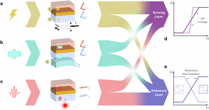
These changes can be induced by: (a) Electrical fields, either using electrical current for spin-orbit torque or voltage-controlled magnetic anisotropy; (b) Strain into magnetoelastic materials via voltage-actuated magnetoelectric substrates or bending of flexible substrates; (c) Engineering the multilayers to have light-sensitive materials, where magnetization orientation can be switched using ultrafast laser pulses. Using external stimuli together with custom-designed multilayers enables sensing characteristics such as (d) changeable ΔH by directly acting on the sensing layer or (e) re-orientation of the sensitive axis by acting on the reference layer.
Adjustable sensing range on-demand
In section “Open challenges”, we examined both established and emerging strategies for setting ΔH, one of the figures of merit in spintronics sensors. In this section, our focus shifts to exploring innovative methods to embed patterned elements with the capability of changing ΔH, as and when necessary. Such a feature will allow the sensor to respond to evolving requirements, whether they involve an increase or decrease of ΔH or restoring the initial performance following long-term usage. A dynamic way to control ΔH is via modification of the magnetic anisotropy by voltage90, strain due to electrical fields91 or mechanical actuation91,92 [Fig. 3a, b]. Voltage-controlled magnetic anisotropy can be used to effectively modify the magnetization orientation of a ferromagnetic thin film adjacent to MgO and has been heavily pursued for memory applications.90. For sensors, altering the bias voltage strength and the polarity applied at the multilayer terminals enabled the control of ΔH and sensitivity93. Naik et al. showed that with a CoFeB sensing layer thickness of 1.7 nm, R(H) evolved from 3 mT coercivity (+1 V), to a linear dependence with ΔH of around ±6 mT for 0.05 V, increasing by 4x to about ±25 mT for −1 V93. In contrast, for 1.6 nm thickness, a ΔH of only ±4.5 mT was obtained with −1 V. This example of voltage actuation in TMR sensors shows a very narrow thickness-to-voltage window to tune ΔH and so far with strongest effect for multilayers with perpendicular magnetic anisotropy, limiting in part their implementation to fully in-plane magnetized systems.
The strain induced by applying mechanical stress is another way to alter the magnetic characteristics of MR sensors92. For this purpose, the multilayers are grown on flexible substrates and bent [Fig. 3b]. This action alters the total magnetic anisotropy energy, changing the magnetization orientation at zero field. By applying a tensile strain in GMR spin valves, Matsumoto et al. were able to make R(H) linear with ΔH of around ±32 mT for a strain of 0.5% and increase by 2x for 0.9% strain [Fig. 4a]94. Their multilayer included magnetostrictive Co in the sensing layer, and the NiFe (with almost null magnetostriction) in the reference layer rendered it strain-insensitive. These changes are usually not permanent, with the sensor reverting to its initial state when the substrate returns to a flat position. Multiple mechanical actuation cycles by bending or stretching the sensing structures can lead to MR degradation and coercivity increase due to cracks and defects. Therefore materials and devices have to be designed to showcase long term performance resilience to bending deformation11.
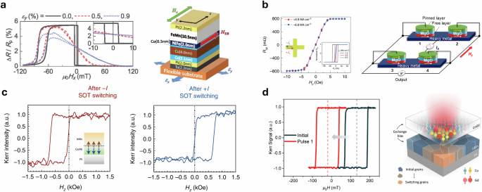
a Bending induces strain in a GMR spin valve and changes ΔH (Reprinted from ref. 94 with the permission of AIP Publishing); (b) Using electrical currents—left—to linearize ΔH via SOT (Reproduced with permission from ref. 39. All rights reserved), which inspired the design of a three terminal TMR sensor—right (Reprinted from35 with permission of AIP Publishing). c SOT driven by electrical currents can also switch the exchange-bias orientation in a bilayer—bottom (Reproduced from100 with permission from SNCSC); (d) Reversal of the exchange-bias orientation by a single-shot ultra-fast laser pulse in a ferrimagnetic/AFM bilayer (Reprinted from101 under the CC-NC-BY license with no modifications).
Following demonstrations in TMR for memory and logic1,95, strain-mediated magnetoelectric coupling appears as a promising method for integration into adjustable sensing platforms [Fig. 3b]. Wang et al. showcased the ability to alter the anisotropy in GMR sensors grown on piezoelectric substrates91. They showed a 6x increase in the ΔH compared to the initial state when actuating the substrate, to a maximum of ±12 mT. However, a slight reduction of ~1% in MR and noticeable coercivity (~2 mT) were also present. Despite these challenges, this method offers compatibility with standard patterning processes and room for improvement at the materials level.
Whatever novel or nano-engineered materials one considers for creating changeable ΔH, their first requirement is to be compatible with GMR and TMR thin-film technology, thereby leveraging their advantages. In that regard, using piezoelectric or flexible substrates with magnetostrictive materials in the multilayer is straightforward and fully compatible with spintronic sensor thin-film systems. However, more information regarding their impact on the intrinsic noise level is still lacking.
3D vector field sensing in a single-element
GMR and TMR sensors perceive the magnetic field as a scalar, measuring only its intensity along a fixed direction defined by the reference layer axis [③ in Fig. 1a]. This feature, however, neglects the fact that the magnetic field is a vector, and it has three components at each point in space. In applications where magnetic fields are employed as a contactless and non-invasive means to extract information, a complete vector field reconstruction can provide more information than the individual components by themselves. Therefore, vector sensors can further enable applications that detect very small fields on highly localized length scales, as in biomedicine4 or non-destructive testing of faults in packaged chips96.
In spintronic sensors, acting directly on (overrightarrow{M}) orientation of the reference layer during fabrication [③/④ in Fig. 1a], is perhaps the most straightforward way to achieve multiaxial sensitivity. Conventional strategies to fabricate adjacent elements with 90° or 180° rotated reference axes, include two-step depositions97 or a localized annealing in a magnetic field98,99. Alternatively, the use of shapeable substrates has provided another dimension for reference axis manipulation. Becker et al. have demonstrated self-assembling devices that roll or fold themselves out of the plane into a three-dimensional platform, thus physically reorienting the reference axis12,13.
In these examples, the sensing elements are not in the same place, creating different detection points in space. Therefore, better spatial accuracy can be achieved if one element could sense all components of the field. For that, an external trigger can be used to reconfigure the sensitive axis orientation, as proposed in Fig. 3a–c.
Three-dimensional magnetic field detection in a single element has been shown with SOT-enabled sensors38,39. The electrical current is here used to linearize the output [Fig. 4b; see section “Background”], and its direction on the Hall bar dictates the vector component of the field being measured. The devices present distinct ΔH depending on the orientation of the field (in-plane, IP, or out-of-plane, OOP), with ref. 39 reporting ΔHIP of ±0.4 mT and ΔHOOP of ±1 mT, and Koraltan et al.38 widening these ranges by about 30x. The main limitations include complex electrical read-out to reconstruct the complete local field vector, and low output signals intrinsic to the operation mechanisms35. As an outlook, hybrid SOT/MR devices are used in magnetic memories41. In sensing, combining SOT/MR can merge the high signal output of TMR with the linearization for OOP field detection enabled by SOT [Fig. 4b].
In order to equip individual MR elements with multi-axis sensitivity, the exchange-bias (Hex) orientation has to be changed. Lin et al. showed perpendicular Hex switching in Co/MnIr bilayers using SOT100, with Hex changing between ≈±350 mT depending on the sign of the current [Fig. 4c]. This year, Guo et al. reported the reversal of perpendicular Hex in a CoGd/MnIr bilayer, using a single femtosecond (40 fs) laser pulse [Fig. 4d]101. Ultrafast magnetization reversal in CoGd is driven by exchange of angular momentum between the Co and Gd atoms, enabled by very fast heating to highly elevated electron temperatures. The existence of interfacial exchange coupling with the MnIr causes a reversed Hex to be imprinted in the antiferromagnet. The authors reported that Hex changed from ≈154 mT to −26 mT, reversing the signal but decreasing its intensity by 6x. Nevertheless, the modulation of the Hex orientation was demonstrated upon consecutive pulses, with no further loss of pinning strength. Both these strategies, SOT and ultrafast laser pulses, show a non-volatile and repeatable reversal of Hex.
However, considerations regarding materials engineering are necessary for their integration into existing MR sensing stacks. Thickness and compositional gradients in multilayers102 allow the combination of the best magneto-electrical properties near the spacer (large MR), while simultaneously exploring different ways to optimize (optical) switching characteristics (e.g., adjustable ΔH, switchable Hex), further away from critical points in the stack. To improve optical switching in TMR for memory applications, Salomoni et al. used 5 repetitions of Tb/Co, retaining MR of up to ~60%103, and Wang et al. used Gd/Co with TMR ~30%104.
Finally, the ability to alter the reference axis on demand, especially in a final packaged device, would be useful in designing novel sensing features. Foreseeable challenges to enable applications include limitations in thermal stability, loss in pinning strength, and possible decrease in the output signal. Nevertheless, the prospect of bridging various technologies (e.g., ultra-fast optics) into the domain of spintronic sensors brings us one step closer to hybrid technology integration.
Sensing devices with additional functionalities
Novel schemes that integrate sensing and computing within the same element are promising alternatives to reduce the amount of transferred data and the complexity in processing it105,106. Unlike conventional systems, where sensory analog information is converted to digital before computing, this approach allows sensors to not only respond to external stimuli but also to process information, thus reducing power consumption, time delay, and footprint105,107. Therefore, these in-sensor computing solutions can significantly impact data-intensive applications or those requiring fast decisions, such as autonomous driving or robot control105,106.
Spintronic sensors, widely used in the mentioned applications19 and originally designed as single-purpose (magnetic field to electrical output transducer), could benefit from embedding additional functionalities, such as logic, memory, or communication [Fig. 5a]. Schulman et al. showed a TMR device that delivers simultaneously a linear output for magnetic field sensing, and a resistive memory depending on the applied electric field108. After electroforming the MgO in the barrier, R(H) curves ranging from flat to ΔH ≈ ±7 mT were observed. These were recorded at intermediate resistance states accessed via different voltage pulses [Fig. 5b]. Chavent et al. expanded functionality by demonstrating a TMR element capable of field sensing, storage, and radio-frequency signal generation, all obtained from the same standard multilayer85. Opening other possibilities, Lv et al. showed the feasibility of embedding a phase-change material such as vanadium dioxide within a TMR multilayer109. The devices were sensitive to both the light and magnetic field, and engineered for latching switches and logic operations.
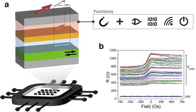
a Concept of an array of sensors on-chip, where each element not only detects magnetic field but is also able to perform additional functions. b Example of a multifunctional device output capable of magnetic field sensing with variable ΔH and MR, according to the non-volatile resistive memory state. Image from ref. 108 under the CC-NC-BY license with no modifications.
These are just first steps towards incorporating computing capabilities into MR elements or arrays. Further progress beyond simple proof-of-concept will need innovative and overarching approaches. These may include the use of new materials or the development of ingenious device layouts, plus their integration with circuit and system designs105,106. We hypothesize that strategies delineated in the above sections for creating and adapting sensing features may catalyze novel concepts for multifunctional (even multimodal) sensors.
Outlook
GMR and TMR spintronic sensors offer unique opportunities to develop advanced sensing instruments. The multilayer structure is the basic building block. Its design defines the limits of performance while also offering a flexible platform for embedding additional functions. Keeping in mind the requirements for final applications will also ensure that the developed solutions yield maximum impact.
Level of technological development
The research area of spintronic sensors presents significant opportunities at all stages of development, from exploratory and fundamental studies to close-to-market readiness.
As examples, emerging commercial products incorporate vortex structures at the GMR sensing layer110, or make use of out-of-plane magnetized references in TMR for detection of the z-component of the field (e.g., XtremeSense®). At an intermediate stage, we can consider those approaches that have made significant scientific progress but have not yet moved beyond lab-scale demonstrations. These include most of the materials and device engineering for low noise applications4,17, the use of electrical currents for linearization via SOT38, and sensing in flexible substrates11.
Still, most strategies discussed are being studied for potential use in spintronic sensors. They are presented as alternatives to achieve the proposed goals, while being compatible with sputter-deposited MR multilayers. However, their use may impair other figures of merit in sensing and thus limit the number of suitable applications. Examples include the use of oblique deposition54 or highly interface-dependent effects (e.g., SOT111) which can weaken thermal stability, or embedding artificial defects, which can reduce the output signal.
Progress in spintronic sensing will also depend on the practical feasibility of unconventional approaches (e.g., ultrafast laser re-pinning101, 2D materials69, 3D nanopatterning71). It will be driven by technological advances in sample preparation, hand-in-hand with a deeper understanding of the physical mechanisms towards precise control and manipulation of the magnetic/electrical behavior. We anticipate that machine learning methods can assist in the design of novel materials112, multilayers, device architectures, and fabrication process113, which often require extensive experimental tests. These methods can also be faster in evaluating relevant trade-offs for sensing and help in reducing the amount of critical materials used114. Finally, we also envisage the ample impact of 2D materials in providing new solutions for next-generation spintronic sensors, possibly at the interface of memory and logic70.
Impact on applications
Pushing the performance limits is particularly relevant in the pursuit of room-temperature, compact, portable, and ultra-sensitive platforms capable of measuring low magnetic field signals. Examples of such applications include the detection of heart signals4 and in-vivo neuronal recordings115. These serve as performance stepping stones for the non-invasive mapping of brain signals116. Overcoming all the open challenges discussed in section “Open challenges” is essential to satisfy the sensitivity (pT to fT) requirements of these demanding applications. Nevertheless, given the minute magnitude of the field to be detected, final systems used outside controlled laboratory environments must consider other effects such as temperature fluctuations117, environmental noise118, and humidity on measurement accuracy.
We also consider a MR sensor that can adjust its sensing range to, for example, detect varying quantities of magnetically labeled biological entities. Through the use of an external trigger, the sensor could transition from a narrow ΔH < 1 mT, suitable for measuring minute quantities of magnetic particles, to ΔH up to 10–100x larger, thus detecting larger volumes without reaching saturation. ΔH changes of this magnitude would be a breakthrough in MR sensors, with changes of up to ~5x reported so far in GMR.
Furthermore, being able to perform accurate and reliable measurements with variable sensitivity, in real time, and in the same platform, could pioneer versatile monitoring instruments. This versatility potentiates their use in a variety of scenarios, from specific medical treatment protocols to the detection of various levels of contaminants in water.
Detecting the magnetic field vector components in three dimensions, at the same point in space, will yield solutions for highly spatially resolved static mapping (e.g., faults in interconnects) and allow remote motion detection of objects with precise pinpointing of their position and rotation (e.g., vehicle detection)8. We discussed ways to reorient the sensitive axis in spintronic sensors either by electrical field actuation, which is complementary-metal- oxide-semiconductor compatible or by bridging into the optics field, expanding possibilities for hybrid technology integration119. This is still an emerging area of research in MR sensing, where the maturity of conventional technology can accelerate developments.
As conclusion of our vision for the future of spintronics sensors is a system that can profit from having enhanced performance and reprogrammable characteristics. This new paradigm of in-sensor computing combines sensing and processing within the same device hardware. Its exploration using MR platforms has only just started.
Conclusions
We have proposed alternatives and innovative approaches to enhance the capabilities of GMR and TMR sensors. We targeted ways to tackle ongoing challenges in increasing field sensitivity, via tuning sensing range, improving the limits of detection, and amplifying the output signal.
Our envisioned solutions rely on the main advantages of these spintronic sensors. These include the versatility of engineering physical properties within the thin film multilayers, alongside easy miniaturization and fabrication processes that allow seamless integration with other technologies. The MR multilayers also provide a foundation for expanding sensing possibilities, namely into the design of on-demand adaptable ΔH and re-orientation of the sensitive axis, moving towards multifunctional devices. Still, major breakthroughs in this field will entail the use of alternative materials systems, novel devices architecture, and unconventional fabrication methods, for which the compatibility with the thin-film stacks can be leveraged.
With this perspective, we aim to inspire the research community to explore new ways in which GMR and TMR sensors can drive the development of innovative magnetic field sensing solutions, to meet the current and evolving needs of various research areas and industries.

Responses