Enhancing X-ray generation from twisted multilayer van der Waals materials by shaping electron wavepackets

Introduction
Bilayer van der Waals (vdW) materials are an emerging class of materials whose name is derived from the fact that they comprise two layers of two-dimensional materials bonded by weak vdW attractive force. Twisted bilayer vdW materials are formed when these two atomic layers are twisted at different orientations with respect to each other, which can cause significant changes in their optoelectronic properties. One of the most popular twisted bilayer vdW materials is twisted bilayer graphene (TBG). At certain so-called magic twist angles, the optoelectronic properties of TBG are substantially altered, leading to important phenomena such as superconductivity, interaction-induced insulating states, extremely flat bands, etc.1,2,3,4,5,6,7,8,9. Bilayer transition metal dichalcogenides (TMDs) vdW materials like WSe2, WS2, MoSe2, and MoS2 at magic twist angles possess unique optoelectrical properties that closely depend on their chemical composition10,11,12,13,14,15,16,17,18,19,20. Research on twisted bilayer vdW materials has revealed their enormous potential to improve the performance of optoelectronic devices, including photodetectors21,22, integrated circuits23,24, photovoltaic cells25, light-emitting diodes26, and nanolaser27. Recent development of fabrication techniques at the atomic scale has further advanced the engineering of twisted multilayer vdW materials, leading to the birth of twistronics, which aims to control and exploit unique physical phenomena emerging at magic twist angles between multiple adjacent layers28,29,30,31,32,33,34,35,36,37,38,39,40.
Whereas TBG, twisted bilayer TMDs and twisted multilayer vdW heterostructure have been extensively studied for a variety of applications in the optical regime, the study of these materials as free electron-driven sources of X-rays remains to be undertaken. Specifically, the role of the twisting geometry in bilayer vdW materials for free electron-driven light emission in these materials, especially in the hard X-ray regime, has yet to be explored. X-rays are essential tools in cutting-edge modern science and industry for applications such as X-ray spectroscopy41,42, X-ray crystallography43,44,45, X-ray computed tomography46, materials characterization47, etc. X-rays also serve life-saving purposes in the medical sector in the form of radiography and radiotherapy48,49,50, providing critical health information and treatments for diseases like cancer. Conventional X-ray sources such as X-ray tubes are limited in tunability, whereas more expensive devices like synchrotron can generate tunable X-ray but is generally massive. This has motivated efforts to find innovative solutions for more versatile sources of tabletop X-rays.
The unprecedented study of free electron-driven twisted multilayer materials as X-ray sources, which is the topic of this paper, is further motivated by a rich field of research in free electron-driven X-ray sources. This includes free electrons propagating through a vdW single-crystals and heterostructures which comprise multiple atomic layers vertically stacked upon each other, have opened a new gate to generate tunable X-ray51,52,53,54,55,56,57,58. Other noteworthy X-ray generation mechanisms include Smith–Purcell emitters59,60,61, light wells62, free-electron lasers63,64,65, inverse Compton scattering66,67, high-harmonic generation68,69,70,71, plasmon polaritons72 and vacuum forces73. These studies have been expanded to explore the effects of electron waveshaping as a robust means of tailoring various quantum electrodynamics (QED) processes74,75,76,77,78,79,80,81. For example, the directionality and intensity of free electron X-rays generated from vdW materials can be tailored, by shaping the electron wavepackets to spatially overlap with the atomic lattice81. The shaping of electron spatio-temporal profile can be achieved using static field82,83,84,85, laser pulses86,87,88,89, surface plasmon polaritons (SPPs)90, phase masks and programmable phase plates91,92,93,94,95.
In this paper, we investigate the use of the twisted bilayer vdW materials as target materials in free electron-driven X-ray generation. We present an ab initio theoretical model for bremsstrahlung radiation that is applicable to twisted multilayer vdW materials in general. Using this model, we show that the twist angle can be used as a mean to control the relative positions of atomic centers in the crystal, allowing a broad range of possible X-ray profiles to be achieved. Furthermore, this can be combined with the shaping of the free electron’s quantum wavefunction to create X-ray sources that are highly versatile. We show that by twisting the bilayer vdW materials, we are able to control the output X-ray properties to feature enhanced directionality or enhanced intensity. We then extend our study to multilayer vdW materials with different interlayer spacings, i.e., the separation between consecutive atomic layers. Our results reveal that smaller interlayer spacing leads to slower fluctuations with greater shifts in the X-ray emission profile (with respect to X-ray energy and emission angle). We show that the output X-ray intensity scales up as an increasing number of atomic layers in the twisted multilayer vdW materials, providing an intuitive and effective way to enhance the output X-ray intensity for any shaped X-ray output profile of choice. Our results should pave the way for the use of twisted bilayer and multilayer materials in X-ray generation for X-ray imaging and other applications in areas including medicine, industry, security and fundamental science.
Results
Analytical QED model of bremsstrahlung from twisted multilayer vdW materials
When a free electron is deflected by an atomic potential, the free electron loses energy in the form of bremsstrahlung radiation. X-rays in bremsstrahlung radiation form the basis of our X-ray generation mechanism. Throughout our entire work, we model the bremsstrahlung scattering process based on first principles from quantum electrodynamics (QED). We model the shaped electron wavefunction ({Psi }_{p}), approximating a Bessel beam of order 181, using 6 momentum eigenstates:
where ({u}^{uparrow }(p){e}^{-frac{i}{hslash }{p}^{mu }{x}_{mu }}) is the Dirac equation’s planewave solution for a single free electron in a definite momentum eigenstate, ({u}^{uparrow }(p)) (={[sqrt{{p}^{mu }{sigma }_{mu }}{xi }^{uparrow },sqrt{{p}^{mu }{bar{sigma }}_{mu }}{xi }^{uparrow }]}^{{rm{T}}}/sqrt{2{p}^{0}}) the Dirac u-type spinor, ({sigma }^{mu }={1,,{sigma }_{x},,{sigma }_{y},,{sigma }_{z}}), ({bar{sigma }}^{mu }={1,,{-sigma }_{x},,{-sigma }_{y},,{-sigma }_{z}}), ({sigma }_{x,y,{z}}) the (2times 2) Pauli matrices, ({xi }^{s}) the spinor where ({xi }^{uparrow }={[1,0]}^{{rm{T}}}) represents spin-up (({xi }^{downarrow }={[0,1]}^{{rm{T}}}) spin-down), (hslash) the reduced Planck constant,({p}^{mu }) the four-momenta, ({x}_{mu }) the spacetime four-vector, and the repeated index convention ({p}^{mu }{x}_{mu }={p}^{0}{x}_{0}-{bf{p}}cdot {bf{x}}) (bold variables denote the three-vector components). The four-momentum ({p}_{m}) for each electron momentum state is given by
where ({E}_{p}) is the electron energy, (left|{bf{p}}right|) the electron momentum magnitude satisfying the energy dispersion relation ({E}_{p}^{2}=) ({left|{bf{p}}right|}^{2}{c}^{2}+{m}_{{rm{e}}}^{2}{c}^{4}) ((c) is the speed of light in free space and ({m}_{{rm{e}}}) the electron mass), ({theta }_{p}) the polar (incident) angle and ({phi }_{p,m}=left(m-1right)2pi /6) the azimuthal angle. The electron’s probability distribution function ({Psi }_{p}^{dagger }{Psi }_{p}) (i.e., electron spatial profile) is specifically shaped to possess identical periodicity as the atomic layer’s lattice vectors (in the xy-plane) while remains invariant along the electron’s main propagating direction (the z-axis).
The total Yukawa potential (in Fourier space ({bf{k}})) of atoms that contribute effectively to the output bremsstrahlung in a twisted ({N}_{{rm{l}}})-layer vdW material (with interlayer spacing ({d}_{z}) = (vert{{bf{d}}}_{z}vert)) is modeled as
with Yukawa potential from (l)th-layer ({a}_{{rm{Yu}},l}left({bf{k}}{boldsymbol{;}},{phi }_{{rm{Twi}},l}right)) oriented at twist angle ({phi }_{{rm{Twi}},l}) as
where ({q}_{{rm{e}}}) is the electron charge, ({varepsilon }_{0}) the vacuum permittivity, ({a}_{0}) the Bohr radius, ({N}_{{rm{a}},l}) the total number of atoms in (l)th atomic layer, (hat{R}({phi }_{{rm{Twi}},l})) the rotation matrix, ({{bf{d}}}_{{n}_{l}}) the lattice vector of ({n}_{l})th atom, ({Z}_{{n}_{l}}) the atomic number of ({n}_{l})th atom associated with screening function parameters ({C}_{{j}_{n}}) and ({mu }_{{j}_{n}}) analytically fitted to Dirac-Hartree-Fock-Slater (DHFS) self-consistent data given in refs. 96,97. Details regarding ({{bf{d}}}_{{n}_{l}}), (hat{R}({phi }_{{rm{Twi}},l})) and ({Z}_{{n}_{l}}), ({C}_{{j}_{n}}), ({mu }_{{j}_{n}}) are discussed in Methods.
The bremsstrahlung differential cross section involving a shaped electron wavepacket (comprising ({N}_{{rm{s}}}) discrete momentum states associated with normalized coefficient ({c}_{m})) and a twisted ({N}_{{rm{l}}})-layer vdW material (with interlayer spacing ({d}_{z}) = (|{{bf{d}}}_{z}{boldsymbol{|}})) is given by
where (sigma) is the bremsstrahlung cross section, ({omega }_{{k}^{{prime} }}) is the angular frequency and (hslash {{k}^{{prime} }}^{mu }) is the four-momenta of the output photon with energy (hslash {omega }_{{k}^{{prime} }}) = (hslash {{k}^{{prime} }}^{0}c) and three-momenta (hslash {{bf{k}}}^{{prime} }) = (left|hslash {{bf{k}}}^{{prime} }right|left{sin {theta }_{{k}^{{prime} }}cos {phi }_{{k}^{{prime} }},,sin {theta }_{{k}^{{prime} }}sin {phi }_{{k}^{{prime} }},,cos {theta }_{{k}^{{prime} }}right}), ({theta }_{{k}^{{prime} }}) (polar angle) and ({phi }_{{k}^{{prime} }})(Azimuthal angle) are the photon emission angles and ({Omega }_{k^{prime} }) the solid angle. ({{p}^{{prime} }}^{mu }) is the four-momenta of the output electron with energy ({E}_{{p}^{{prime} }}) = (sqrt{{left|{{bf{p}}}^{{boldsymbol{{prime} }}}right|}^{2}{c}^{2}+{m}_{{rm{e}}}^{2}{c}^{4}}), three-momenta(,{{bf{p}}}^{{boldsymbol{{prime} }}},)= (left|{{bf{p}}}^{{{{prime} }}}right|{sin {theta }_{{p}^{{prime} }}cos {phi }_{{p}^{{prime} }},,sin {theta }_{{p}^{{prime} }}sin {phi }_{{p}^{{prime} }},,cos {theta }_{{p}^{{prime} }}}) and solid angle ({Omega }_{{p}^{{prime} }}). Unitless Kronecker delta(,{delta }_{{E}_{p}-hslash {omega }_{{k}^{{prime} }}-{E}_{{p}^{{prime} }}}) represents the energy constraint and wavevector ({{boldsymbol{kappa }}}_{m}) = (frac{{{bf{p}}}_{m}}{hslash }-{{bf{k}}}^{{prime} }-frac{{{bf{p}}}^{{boldsymbol{{prime} }}}}{hslash }).
The scattering amplitude ({{mathcal{M}}}_{{k}^{{prime} }{p}^{{prime} }{p}_{m}}^{{r}^{{prime} }{s}^{{prime} }uparrow ,}) is given by
where ({u}^{{s}^{{prime} }}left({p}^{{prime} }right)) the output electron’s Dirac u-type spinor with spin ({s}^{{prime} }), ({epsilon }_{sigma }^{{r}^{{prime} }}) the photon polarization and ({gamma }^{sigma }) the gamma matrices following conventions of Peskin and Schroeder98 (e.g., metric tensor with diagonal elements (left{1,-1,-1,-1right})).
Tailoring X-ray emission profiles
We first present how shaping the electron wavepacket and twisting the bilayer vdW materials (graphene and WS2) can tailor the bremsstrahlung differential cross section ({rm{d}}sigma /left({rm{d}}{omega }_{{k}^{{prime} }}{rm{d}}{Omega }_{{k}^{{prime} }}right)), which is proportional to the output X-ray intensity. Figure 1a, f illustrate the bottom views of twisted bilayer graphene (TBG) and twisted bilayer WS2 at twist angle ({phi }_{{rm{Twi}},l}), respectively. Figures 1b, g depict physical configurations of single 6-state shaped electron wavepacket incident on a TBG and a twisted bilayer WS2, respectively. The TBG has interlayer spacing of 3.4 Å while the twisted bilayer WS2 has a longer interlayer spacing of 6.67 Å. The electron spatial profiles (probability distribution function ({Psi }_{p}^{dagger }{Psi }_{p})) are engineered to form periodic patterns matching the untwisted bilayer graphene and untwisted bilayer WS2 lattice periodicities, as shown in Fig. 1c, h, respectively. Figure 1d, e show the output 15 keV X-ray angular profiles for bilayer graphene with ({phi }_{{rm{Twi}},l}) of 0° (untwisted) and 7.4° (twisted), respectively. Figure 1i, j show the output 15 keV X-ray angular profiles for bilayer WS2 with ({phi }_{{rm{Twi}},l}) of 0° (untwisted) and 4.9° (twisted), respectively. In both untwisted cases (Fig. 1d, i), the shaped electron wavepacket generates X-ray with unidirectionality, i.e., intensity peaks in singular forward direction, compared to cases with unshaped electron wavepacket (Supplementary Information Section 1, Fig. S1). Using the same shaped electron wavepacket, twisting the bilayer vdW materials to specific twist angles (Fig. 1e, j) restores the X-ray directionality but at the same time induces a two-fold enhancement in the X-ray intensity. Also, notice that the bremsstrahlung differential cross section is generally proportional to the square of the atomic number, which explains the much higher X-ray intensity from bilayer WS2 compared to that of bilayer graphene. One can refer to Fig. S2 in Supplementary Information Section 2 to understand the X-ray intensity’s dependence on the twist angle of bilayer vdW material, which the optimal twist angles associated with the highest output X-ray intensity are obtained accordingly. Another interesting aspect is the polarization of generated X-rays, which some important examples are presented in Supplementary Information Section 3.

a Illustrates the bottom view of a twisted bilayer graphene which the two atomic layers (lies in the xy-plane) are twisted in opposite orientation at twist angle ({phi }_{{rm{twi}}}). b Depicts a 20 keV single-shaped electron wavefunction (6-state, incident angle ({theta }_{p}) = 8.03°) propagating in the z-axis toward a twisted bilayer graphene. c Shows the shaped electron spatial profile (probability distribution function ({Psi }_{p}^{dagger }{Psi }_{p})) with periodic patterns, where solid (dashed) gray circles denoting the projections of effective carbon atoms in the first (second) layer. The output 15 keV X-ray angular profiles (differential cross section ({rm{d}}sigma /left({rm{d}}{omega }_{{k}^{{prime} }}{rm{d}}{Omega }_{{k}^{{prime} }}right))) are shown in (d, e) for twist angles of 0° and 7.4°, respectively. f Illustrates the bottom view of a twisted bilayer WS2 and g Depicts a 20 keV single-shaped electron wavefunction (6-state, incident angle ({theta }_{p}) = 9.42°) propagating in the z-axis towards a twisted bilayer WS2. Its spatial profile is shown in (h) where solid (dashed) purple and yellow circles denoting the projections of effective tungsten and sulfur atoms in the first (second) layer, respectively. The output 15 keV X-ray angular profiles (differential cross section ({rm{d}}sigma /left({rm{d}}{omega }_{{k}^{{prime} }}{rm{d}}{Omega }_{{k}^{{prime} }}right))) are shown in (i, j) for twist angles of 0° and 4.9°, respectively. For different twist angle, shaped electron incident on bilayer vdW materials can emit X-ray with either unidirectionality (d, i) or enhanced intensity (e, j), compared to unshaped electron cases.
X-ray intensities’ dependence on interlayer spacing and number of layers
Next, we investigate the role of interlayer spacing ({d}_{z}) in controlling the output X-ray intensity. For simplicity, we consider two carbon atoms aligned on the z-axis in both cases of single 1-state unshaped electron wavepacket (“1-S”) and a single 6-state shaped electron wavepacket (“6-S”), as depicted in Fig. 2a, d, respectively. The corresponding X-ray emission maps for “1-S” (“6-S”) with ({d}_{z}) of 1 and 3 Å are shown in Fig. 2b, c (Fig. 2e, f), respectively. Similar to previous results, unshaped electron wavepacket emits X-ray with intensity peaks at large emission angles (>45°), while shaped electron wavepacket generates more directional X-ray (emitted mostly in the z-direction). It is observed that in all cases, smaller interlayer spacing results in fluctuations (with respect to X-ray energy and emission angle) with lower frequency and greater amplitude, which appear as wider fringes in the X-ray emission map.
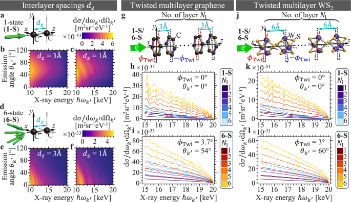
a Illustrates a 20 keV single unshaped electron wavefunction (1-state) propagates toward two carbon atoms aligned along the z-axis with interlayer spacing ({d}_{z}). b, c Show the colormaps (emission angle ({theta }_{{k}^{{prime} }}) against X-ray energy ({E}_{{k}^{{prime} }})) of the bremsstrahlung differential cross section ({rm{d}}sigma /left({rm{d}}{omega }_{{k}^{{prime} }}{rm{d}}{Omega }_{{k}^{{prime} }}right)) for ({d}_{z}) = 3Å and ({d}_{z}) = 1 Å, respectively. Similarly, (d) illustrates a 20 keV single-shaped electron wavefunction (6-state, incident angle ({theta }_{p}) = 15°) and e, f show the corresponding X-ray emission maps for ({d}_{z}) = 3 Å and ({d}_{z}) = 1 Å, respectively. Comparing (c, f) and (b, e), shorter interlayer spacing induces slower fluctuations in the X-ray emission map (with respect to X-ray energy and emission angle). g Depicts a 20 keV electron incident on twisted ({N}_{{rm{l}}})-layer graphene (({d}_{z}) = 3 Å). (h, i) Show the output X-ray intensity scales up with increasing ({N}_{{rm{l}}}) for both unshaped “1-S” and shaped “6-S” (incident angle ({theta }_{p}) = 16.22°) electron wavepackets, at twist angles ({phi }_{{rm{Twi}}}) of 0° (emission angle ({theta }_{{k}^{{prime} }}) = 0°) and 3.7° (({theta }_{{k}^{{prime} }}) = 54°), respectively. j Illustrates 20 keV electron incident on twisted ({N}_{{rm{l}}})-layer WS2 (({d}_{z}) = 6 Å). k, l Show the output X-ray intensity scales up with increasing ({N}_{{rm{l}}}) for both “1-S” and “6-S” (({theta }_{p}) = 15.77°) electron wavepackets, at ({phi }_{{rm{Twi}}}) of 0° (({theta }_{{k}^{{prime} }}) = 0°) and 3° (({theta }_{{k}^{{prime} }}) = 60°), respectively.
We now extend our studies to twisted multilayer graphene and twisted multilayer WS2, which their corresponding physical configurations are illustrated in Fig. 2g, j, respectively. The atomic layers are twisted alternatively in opposite orientation, i.e., for twist angle ({phi }_{{rm{Twi}}}) the (l) th-layer is twisted at ({left(-1right)}^{l-1}{phi }_{{rm{Twi}}}). The output X-ray differential cross sections for twisted multilayer graphene at different X-ray energies (for both “1-S” unshaped electron wavepacket and “6-S” shaped electron wavepacket) are plotted in Fig. 2h (untwisted ({phi }_{{rm{Twi}}}) = 0°, emission angles ({theta }_{{k}^{{prime} }}) = ({phi }_{{k}^{{prime} }}) = 0°) and 2i (twisted ({phi }_{{rm{Twi}}}) = 3.7°, emission angles ({theta }_{{k}^{{prime} }}) = 54°, ({phi }_{{k}^{{prime} }}) = 0°). The corresponding plottings for twisted multilayer WS2 are presented in Fig. 2k (untwisted ({phi }_{{rm{Twi}}}) = 0°, emission angles ({theta }_{{k}^{{prime} }}) = ({phi }_{{k}^{{prime} }}) = 0°) and 2 l (twisted ({phi }_{{rm{Twi}}}) = 3°, emission angles ({theta }_{{k}^{{prime} }}) = 60°, ({phi }_{{k}^{{prime} }}) = 0°). In all cases, the output X-ray intensities always scale up as the number of layers ({N}_{{rm{l}}}), even in lower energy regime down to 5 keV (shown in Supplementary Information Section 4). Compared to twisted multilayer graphene with shorter interlayer spacing of 3 Å, the fluctuations in X-ray intensity (with respect to X-ray energy) for twisted multilayer WS2 oscillate faster with lower amplitude due to a longer interlayer spacing of 6Å, which is consistent with previous findings. One can also observe that in both cases of graphene and WS2, the fluctuations in X-ray intensities (with respect to X-ray energy) tend to vanish at larger twist angle, due to misalignment of atomic potentials along the longitudinal direction.
Discussion
To study shaped free electron radiation from twisted bilayer vdW materials, we adopt the “double-twisting” model, wherein the two atomic layers are twisted in opposite orientations simultaneously. This model preserves the geometrical angular symmetry in the xy-plane for mathematical convenience, and allows one to control the symmetry of the output X-ray emission profile. Due to the hexagonal lattice structure of the graphene and WS2, we choose to use shaped electron wavepacket comprising 6 specific momentum states with identical incident angle ({theta }_{p}). The electron spatial profile can thus be conveniently engineered via varying ({theta }_{p}) to match the lattice vectors of different bilayer vdW materials. The electron spatial profile is invariant along the z-axis, i.e., longitudinally identical in the vicinity of every effective atomic centers of the vdW materials. This guarantees the optimization of the desired output X-ray emission profile by eliminating unwanted interference due to a mismatch between the electron spatial profile and atomic potentials.
The emergence of fluctuations in the output bremsstrahlung X-ray emission map with respect to X-ray energy and emission angle is fully deterministic, i.e., not due to noise or other sources of randomness, but instead a signature of the interference between the atomic potentials in Fourier space, which mathematically translate to expressions of phasors in Eqs. (3) and (4). The frequency and amplitude of the fluctuations are shown to be sensitive to the interlayer spacing between the atomic layers in vdW materials, but they do not significantly alter the overall directionality of the output X-ray. Although these fluctuations are affected by the interlayer spacing, to our best knowledge, in this paper, there is no intuitive way to precisely manipulate them. Nevertheless, future works can be carried out to model these fluctuations, which we believe can lead to even stronger output radiation under coherent control of relevant constructive interference.
Let us now address the importance of the twisting geometry of the bilayer vdW materials. At certain choices of twist angle, the atomic centers of the atoms (carbon for bilayer graphene, tungsten and sulfur for bilayer WS2) tend to align with the intensity peaks of the shaped electron’s spatial profile, and thus lead to the transformation of the X-ray emission profile from “unidirectional” mode to “intensity-enhanced” mode. On the contrary, for an unshaped electron wavepacket, twisting the bilayer vdW materials does not induce any significant change due to the uniform distribution of electron spatial profile (shown in Supplementary Information Section 1 Fig. S1). Therefore, both twisted bilayer vdW materials and shaped electron wavepacket are essential to realize the “transformation” phenomenon of the output X-ray profile. The twisting geometry provides greater control over tunable X-ray, especially in the scenario where only a certain shaped electron wavepacket is available. Moreover, the twisting of vdW materials generally does not occupy extra operational spaces, which could be advantageous comparing to tunable PXR, which sometimes requires tilting of the crystal.
Additionally, the twisting geometry of bilayer vdW materials can also be used to control the polarization of the generated X-ray, which is an important feature that can potentially lead to a wide range of applications. As presented in Supplementary Information Section 3, our results provide a first glimpse of how a combination of shaped electron wavefunction and twisted bilayer crystal can transform the X-ray from circular polarization to linear polarization (or the other way around). A more quantitative mechanism based on bilayer materials to tailor X-ray polarization is yet to be studied and is not within the scope of this paper, but we believe it deserves to be explored in more detail in future work.
In conclusion, our studies on twisted bilayer and multilayer vdW materials with shaped electron wavepackets have led us to present a versatile method of tailoring bremsstrahlung X-rays. Based on first principles QED, we have computed the bremsstrahlung differential cross section considering arbitrarily shaped electron wavepackets and multilayer vdW heterostructure with arbitrary twisting geometries. Apart from shaping the electron wavepacket, the twisting geometry of vdW materials can provide extra degrees of freedom to tailor free electron radiation. By increasing the twist angle between two adjacent atomic layers, the output X-ray profiles can be transformed from “directional” mode to “intensity-enhanced” mode. This is due to the change of overlap conditions between the atomic centers and electron probability distribution. We have outlined the importance of having a non-uniform electron spatial profile, i.e., shaped electron wavepacket, which is crucial for achieving such transformation. Significantly, we have extended our studies to twisted multilayer vdW materials. Our results show that it is feasible to scale up the output X-ray emission by increasing the number of twisted atomic layers, while preserving its transformation features as seen in twisted bilayer vdW materials. Our work also investigated the dependence of interlayer spacing of multilayer vdW materials, showing that a decrease in interlayer spacing results in greater but slower fluctuations in the output X-ray intensity as a function of X-ray energy and emission angle. These fluctuations tend to vanish at large twist angles, due to misalignment of atomic centers across different layers. Our findings show how the combination of free electron waveshaping and twisted multilayer materials can result in enhanced control over the output of X-ray sources, for applications ranging from medical imaging to industrial inspection.
Methods
Multilayer graphene
The lattice basis vectors of multilayer hexagonal crystalline structure are modeled as
where (a) is the lattice constant ((a) = 2.46 Å for graphene, (a) = 3.15 Å for WS2) and ({d}_{z}) is the interlayer spacing.
For each layer of graphene, there are two carbon atoms per unit cell. The lattice vectors of carbon atoms in ({n}_{l}) th unit cell of (l) th-layer graphene are modeled as:
where (a) = 2.46 Å, ({n}_{a}), ({n}_{b},{mathbb{in }},{mathbb{Z}}) and (l) (in {{mathbb{Z}}}^{+}). The atomic number of carbon ({Z}_{{rm{C}}}) = 6 and screening parameters ({C}_{1,2}) = {0.1537, 8.0404}, ({mu }_{mathrm{1,2}}) = {0.8463, 1.4913}96,97.
Multilayer WS2
For each layer of WS2, there are one tungsten atom and two sulfur atoms per unit cell. The lattice vectors of tungsten atoms and sulfur atoms in ({n}_{l})th unit cell of (l)th layer WS2 are modeled as:
where (a) = 3.15 Å, ({n}_{a}), ({n}_{b},{mathbb{in}},{mathbb{Z}}) and (l) (in {{mathbb{Z}}}^{+}). The atomic number of tungsten ({Z}_{{rm{W}}}) = 74 and screening parameters ({C}_{1,2,3}) = {0.15, 0.6871, 0.1629}, ({mu }_{mathrm{1,2,3}}) = {28.63, 4.2426, 1.234}96,97. The atomic number of sulfur ({Z}_{{rm{S}}}) = 16 and screening parameters ({C}_{1,2,3}) = {0.5459, −0.5333, 0.9874}, ({mu }_{mathrm{1,2,3}}) = {6.3703, 2.5517, 1.6753}96,97.
Rotation matrix
To model the twisting of multilayer vdW material in the xy-plane, we apply the rotation matrix (hat{R}({phi }_{{rm{Twi}},l})) to the lattice vectors of atoms in (l)th-layer as
where ({phi }_{{rm{Twi}},l}) is the twist angle for (l)th-layer of the vdW material. For mathematical convenience, we model the twist angle of bilayer vdW material as ({phi }_{{rm{Twi}},1}=-{phi }_{{rm{Twi}},2}={phi }_{{rm{Twi}}}ge 0), i.e., the relative angle between the two atomic layers is always (2{phi }_{{rm{Twi}}}). Similarly, the twisted multilayer vdW material has (l)th-layer oriented at twist angle ({phi }_{{rm{Twi}},l}={left(-1right)}^{l-1}{phi }_{{rm{Twi}}}), i.e., the relative angle between two adjacent atomic layers is (2{phi }_{{rm{Twi}}}).


Responses