First principles calculations of carrier dynamics of screw dislocation

Introduction
Nonradiative carrier recombination (NCR), as described by the Shockley-Read-Hall (SRH) model and multi-phonon emission process1,2, has recently drawn wide range of interests from fundamental semiconductor physics to device applications3,4,5,6,7,8. It plays critical role in determining the semiconductor device efficiency, from detector, to solar cell, to light emission diode9,10,11,12. However, most theoretical studies are focused on point defects13, such as the calculation although in actually applications, very often it is the dislocation which plays more dominant role. There are at least two factors responsible for the lack of theoretical work. First, to describe a dislocation, a large system with close to 1000 atoms are needed, beyond the size range which can be easily calculated in first principles. Second, the atomic structure of a dislocation core is complicated and often unknown. With the recent development of high resolution of transmission electron microscope (HRTEM), there are more and more cases where the dislocation atomic structures become known14,15,16,17. Meanwhile, as the computer power improves and new computational algorithm developed, we are now being able to deal with 1000 atom systems using density functional theory (DFT)18,19,20.
The first principles calculation of NCR induced by deep-level point defects has been developed recently21, it is based on the multiple phonon coupling theory developed by Huang etc22, including the adiabatic approximation method21, static coupling method23, classical Marcus theory24, and one-dimensional quantum formula method25. All these methods depend on the fact where the defect states are localized in real space. As a result, the occupation of these states can cause an atomic relaxation, the so called reorganization energy in Marcus theory24. This however, might not be true in dislocation where the defect state can be extended along the dislocation line. The c-type (0001) screw dislocation, which we study here, is one of the most common screw dislocations in GaN thin film crystal. Many experimental photoluminescence (PL) of GaN dislocation show that there is a dark spot of PL near each dislocation line26,27,28,29,30. While some experiments point out that the screw dislocation is a NCR center, while edge dislocation is not27,28, but the opposites claims also exist30, and there are also experiments showing that the screw dislocation is not the main NCR center15,16. All this highlights the importance of theoretical investigations.
In this work, we developed a large-scale nonadiabatic molecular dynamics (NAMD) method to calculate the nonradiative carrier decay, which shows low computational costs when applied to thousand-atom systems. We also developed a position patching scheme to get the atomic position of a large system under thermal equilibrium, and a dynamic matrix patching method to calculate the phonon spectra of large dislocation supercell. The combination of these methods allows us to study the electronic structure and carrier dynamics of the large dislocation problems. We have modeled the structure of the screw dislocation of c-type (0001) GaN and calculated the nonradiative decay. The calculation shows a 0.6 eV band gap in the core level states, but it is not a phonon bottleneck. Large-scale NAMD simulations reveals that the nonradiative transition life time between dislocation core states is in the picosecond scale at room temperature, highlighting the screw dislocation to be an efficient carrier killer with a large cross section.
Results and discussion
The structure model
To construct a c-type (0001) screw dislocation for first-principles calculation, a supercell-cluster hybrid model31 with 464-atom GaN supercell (8×6×1) is made. The use of this model is to avoid the compatibility problem of periodic boundary condition and screw dislocation burgers vector. The vacuum space is set to 10 Å in order to place the system in a periodic box for plane wave DFT calculations and the surface is passivated using fractional charge pseudo-hydrogen atoms. The DFT relaxed equilibrium lattice parameters of bulk GaN (a = b = 3.19 Å, c = 5.189 Å) agree well with the experimental result32. The calculated elastic constants and the phonon spectra of bulk GaN are also presented. (Supplementary Table 1 and Fig. 2b). A full-core screw dislocation with a burgers vector of b = c[0001] is embedded at the center of the nanowire along (0001) direction of the wurtzite crystal structure (Fig. 1a, b), which agrees with the experimental HRTEM observations (Fig. 1c, d). Seen from the HRTEM images, the core structure is stoichiometric (full core). Note, the HRTEM image may indicate either double 6-atom-ring core33,34 or single 6-atom-ring core35. To simplify the issue, we adopt the widely used single 6-atom-ring full-core model as a test case for our study (more discussion see Supplementary Note 1).

a, b Top and side view of a full-core screw dislocation in GaN nanowire, with green, purple and pink balls representing Ga, N and H atom, respectively; the red dashed circle marks the potion of the dislocation core. c Scanning transmission electron microscope (STEM) image of a full-core screw dislocation in GaN14, adapted with permission from ref. 14 Copyright 1998 AIP publishing. d Side view of full core screw dislocations with arrow (mathop{c}limits^{ rightharpoonup }), and (mathop{n}limits^{ rightharpoonup }), indicating the position of the dislocation core; (mathop{g}limits^{ rightharpoonup }) is a vector along [0001] direction17, adapted with permission from ref. 17 Copyright 2001 AIP publishing. e Side view of the wave function at VB (state 3) for the GaN dislocation nanowire. f The band structure and DOS of perfect GaN nanowire. g The band structure and DOS of GaN nanowire with the screw dislocation. h, Top view of wave functions for the six band-gap states marked in corresponding band structure of the GaN dislocation nanowire.
The electronic structure
Figure 1g shows the band structure and density of states (DOS) of GaN nanowire with the screw dislocation. Note, to correct the DFT band gap error, we have modified the nonlocal part of Ga pseudopotential through changing the Dij diagonal element in the UPF pseudopotential format36,37, which is similar in spirit to Segev’s work38, so the bulk GaN band gap is 3.49 eV, in agreement with experiments39,40. This modification mostly changes the conduction band, thus has minimum effect on the occupied state behavior and the relaxed atomic structures. Compared to the electronic structures of the perfect GaN nanowire (Fig. 1f), it is clear that there are 6 in-gap bands corresponding to the dislocation core defect states, with their wave functions shown in Fig. 1h. For a neutral system, three of these bands are occupied, and the other three are unoccupied, and there is a 0.6 eV gap between the occupied and unoccupied state. If the GaN is n-type, then the upper defect states will become partially occupied, and the states become metal41. Such metallization can help the dislocation to trap the carriers. It is clear that all of these states are highly localized around the dislocation line within about 0.5 nm surrounding the core.
It is obvious that during the carrier dynamics, the electron or hole carriers can quickly slide down (cooling) along the band structure line due to electron-acoustic phonon interaction. Thus, the only issue is, whether the carrier can jump over the 0.6 eV band gap for electron-hole nonradiative recombination (i.e., whether there is a phonon bottle-neck). The 0.6 eV is a few times of the highest phonon mode energy in GaN (which is about 0.08 eV). For point defect, it is usual to use the Kun Huang’s formula, or many other similar formulas to calculate NCR, provided one of the transition electronic states is localized in space so the so-called reorganization energy and the atomic structure change after transition is not zero. However, if both the electronic states before and after the transition is extended, such reorganization energy will be zero. In such cases, the transition will happen only through high order perturbation caused by the coupling constant (leftlangle aleft|frac{partial H}{partial {R}_{i}}right|brightrangle), instead of phonon mode wave function mis-alignment after the electron transition. To describe this higher order perturbation transition between extended state a and b, one can used the NAMD formalism42 under the classical path approximation, where the atomic position dynamics is not influenced by the carrier dynamics.
To determine which method one should use, we need to find out whether the dislocation state is localized along the line. This is possible since for one dimensional (1D) state, in theory, any small potential fluctuation in the 1D direction can cause the band edge state to become localized43,44. To answer this question, we developed a position patching scheme to get atomic position of a large system under thermal equilibrium and calculated the band edge states. We have constructed a large 8×6×10 system atomic configuration (with 4640 atoms, and the 10 is in the dislocation line z direction), where ten 8×6×1 systems with atomic displacement at T = 300 K are merged together along z direction. Before doing the merge, we first carried out 3000 fs MD on the 8×6×1 system to obtain 10 configurations (snapshots) with time interval of 300 fs to avoid any correlations between the configurations. We have multiplied the atomic displacement by a mask function for each of the configuration, then add them together, to get:
Where (Delta {R}_{i}^{{prime} }) is the merged atomic displacement of atom i and (Delta {R}_{i}(l)) is the atomic displacement of snapshot l and atom i (the atomic index i has been periodically extended from the 8×6×1 system to 8×6×10 system). ({widetilde{m}}_{l}({z}_{i})) (here zi is the ideal atomic position of atom i) is a Gaussian function expressed as:
Here we set n to the lattice constant c of 5.189. Note, the above procedure can get the atomic displacements of a large system under thermal dynamic fluctuation. After we obtained the atomic configuration, we have used PWmat code45 with Gaussian basis to calculate the SCF-DFT potential of the large system. Note, the latest version of PWmat also includes Gaussian basis calculation following the methodology of CP2K46, which allows calculation of large system. After we get the potential, using plane wave expansion, we calculated the band edge state of the big supercell using the folded spectrum method (FSM)47. The resulting band edge states for the 4640 atomic system are shown in Fig. 1e. One can see that, they are extended over a length of 5.189 nm. Since there is no large fluctuation in the charge density along z-direction, the eventual 1D localization length could be much larger than 5.189 nm, and the reorganization energy with such a weakly localization state should be rather small. This means we should use the NAMD algorithm, instead of localized state algorithm to calculate the state transition rate crossing the 0.6 eV band gap.
The large-scale NAMD simulation on carrier dynamics
Due to the large system, and the necessity to simulate it a long time dynamics, we used a new procedure to carry out NAMD simulation, which is different from the NAMD formalism used in our previous work48 (more discussion see Supplementary Note 2). To carry out NAMD, we need to integrate the time dependent Schrodinger equation (TDSE):
Where the Ψ(t) and H(t) denote the wavefunction and Hamiltonian of the supercell with a screw dislocation. In order to represent the time evolving Hamiltonian, we expand it using a small atomic displacement (ΔR) as:
We will use harmonic approximation to represent the atomic displacement ΔR(t):
Here, K and T are Boltzmann constant and temperature, respectively; μ (Rm, l) is the renormalized phonon mode with the atomic index Rm and phonon mode index l, θl is a random phase of the phonon mode l, and(,{omega }_{l}) is its frequency. Here, we have used the fact each phonon mode will have a kinetic energy of KT to determine its amplitude as (sqrt{{KT}/{omega }_{l}^{2}}). To solve the TDSE, we expand the time evolving wave function under the basis of the static band gap states ({phi }_{i}) (the eigen state of H0):
Placing Eq. (6) into Eq. (4), we can have the time evolution equation of coefficient ci (t). However, in order to introduce the dephasing term, we will use the density matrix Dij(t) under the basis ({phi }_{i}):
Where the h indicates different statistical sampling with weight wh. The time evolution of the Dij(t) can be written as:
where Hij(t) is given by the following formula:
The off-diagonal term of Dij(t) reveals coherent coupling between states ({phi }_{i}) and ({phi }_{j}). It is customarily to introduce a dephasing between these two states by adding a decay term of the off-diagonal term, hence we have48:
Where ({tau }_{{ij}}left(tright)) is the decoherence time between state i and j, which can be estimated from the eigen energy fluctuation between state i and j, we estimated it to be about 150 fs following the equation in Ref. 48, as discussed in Supplementary Note 3. We will study how fast a hole state at the edge of the valence band relaxes into the conduction band. This can be calculated by first placing one hole at the valence band edge state (the Dii(t = 0) = 1 for the given state i, and all the other elements to be zero), and monitoring the sum of conduction band ({sum }_{jepsilon {CB}}{D}_{{jj}}) as a function of time t.
To carry out Eq. (10), we need to calculate (1) all the phonon modes; (2) the electron-phonon coupling constants ({F}_{j,i}(m)=langle {phi }_{j}|partial H/partial {R}_{m}|{phi }_{i}rangle) in advance. We first turn to the calculation of the phonon spectrum of the dislocation supercell. For this simulation, we have used an 8×6×3 supercell with 1392 atoms. All the subsequent NAMD calculations are carried out using this supercell. The phonon spectrum can be calculated through diagonalizing the following dynamic matrix:
Where mi (mj) is the mass of atom i (j). Because (partial E/partial {R}_{i}partial {R}_{j}=partial {F}_{{R}_{i}}({R}_{j})/{partial R}_{j}), we can numerically displace each atoms Rj, while using Hellman-Feynman theory to calculate the atomic forces ({F}_{{R}_{i}}({R}_{j})) for all the atoms Ri. However, for a supercell with 1392 atoms, there will be 1392 × 3 = 4176 self-consistent field (SCF) DFT calculations (each for a 1392 atom system). To reduce this task, we followed the dynamic matrix patching procedure used to calculate the phonon modes of point defects21. More specifically, we divide the large dislocation supercell into three regions: R1 (contains the dislocation core), R2 (a buffer region), and R3 (the outside region) as shown in Fig. 2a. Now we will determine the dynamic matrix (dij) of the large supercell using Eq. (12): 1) When one of i and j is inside R1, the dij equals to the corresponding dynamic matrix of a small dislocation supercell (dij-small) (dislocation system with 576 atoms which can be calculated quickly); 2) when both atom i and j are in R2 or R3 region, the dij equals to the corresponding dynamic matrix of a perfect bulk supercell (dij-bulk); 3) when i, j, one is in R1 and the other is in R3, dij = 0 due to large inter-atomic distance. Figure 2a shows the different cases. Note, the case 1) is the most expensive case where we need to displace all the atoms within the R1 region. In our case, there are 36 nonequivalent atoms inside the R1 region (within one period in the z direction, while the system has three periods). We have used the 576-atom small wire to carry out this calculation. For the bulk, due to the symmetry, we only need to displace one Ga and one N atoms in a 384-atom supercell.
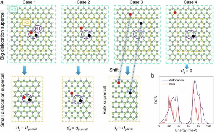
a The four main situations for the determination of the corresponding dij; the purple dashed circle, green and orange and dashed box mark the region of R1 (dislocation core), R2, and R3 respectively; in case 3, the blue dashed arrows indicate the shift of two atoms from the big dislocation supercell to the corresponding positions in the bulk supercell. b The comparison of phonon DOS between bulk GaN and the GaN dislocation supercell with the vertical ordinate rescaled.
After we obtain the dij matrix from Eq. (12), it is necessary to enforce all the symmetry of dij. In particular, we should have: symmetry condition ({partial }^{2}E/partial {R}_{i}partial {R}_{j}=frac{{partial }^{2}E}{partial {R}_{j}partial {R}_{i}}), and the sum rule: ({sum }_{{R}_{i}}{partial }^{2}E/partial {R}_{i}partial {R}_{j}=0). Also note, in the above procedure, we have fixed the surface pseudo-hydrogen atoms, hence they are not in the index i and j. After enforcing these conditions, the phonon spectrum is obtained by diagonalizing Eq. (11). The result shows a few imaginary frequencies which have minimum effect on carrier dynamics, as discussed in Supplementary Note 4 and Supplementary Fig. 1. The calculated phonon DOS is shown in Fig. 2b. This DOS can be compared with bulk GaN phonon spectrum. One major difference is a main peak around 30 meV. The amplitudes of these phonon modes are shown in Supplementary Figs. 2 and 3, and they are mainly near the dislocation core, which are the phonon modes needed to induce the electron state transitions.
The second task is to calculate the electron-phonon coupling constants. One can use numerical approach to calculate (partial H/partial {R}_{m}) by displacing each atom. Such calculation will have the same cost as to calculate the dynamic matrix of the system using the direct method. To avoid that, we have used the special variational algorithm to calculate the electron-phonon coupling21. More specifically, to calculate the coupling between ({phi }_{i}) and ({phi }_{j}), we add an external charge in the self-consistent calculation21, i.e,
here, λ is a small number. Under SCF calculation, we obtain the atom force FR. We can then use numerical difference to calculate dFR / dλ, one can show that:
The advantage of this method is that, from one SCF calculation, one yield all the electron-phonon coupling constants for all atom R for a given i and j pair. This will be efficient if the number of i and j pair is not large. Here, we took three highest valence states and three lowest conduction band states, thus we have done 6×7/2 = 21 SCF calculations using the 8×6×3 supercell to get all the electron-phonon coupling constants needed for our study.
Having obtained the electron-phonon coupling constants and the phonon spectrum, we can now carry out the time evolving calculation for Dij(t) [Eq. (10)] and obtain the hopping rate from a hole in the valence band to the conduction bands. Figure 3 presents the calculated transition probability for an electron transferring from state 3 (top of valence band) to state 4,5,6 with different temperatures. At 300 K, the transition lifetime is calculated as ~ 3 ps. Note, the radiative recombination life time is typically in the order of several ns, thus this phonon assisted nonradiative recombination is much faster than the radiative recombination, hence it is an efficient carrier killer. This result indicates there is no strong phonon bottleneck due to the 0.6 eV band gap. The reason can be attribute to the multiple phonon process. Note, if this is for a bulk material with 0.6 eV band gap, there will be probably some phonon bottleneck (the phonon assisted transition will be slower than the radiative recombination). In dislocation case, the wave functions are localized in the cross section. So, even if it is extended in the z-direction, due to its cross section localization, its electron-phonon coupling effect is probably much stronger than that in the bulk. As a result, the multiple phonon effect is strong. An interesting fact is that, for neutral system, the Fermi energy is within the 0.6 eV band gap. However, for most GaN, the system is n-typed, which means the Fermi energy is close to the bulk conduction band. As a result, the core states above the 0.6 eV band gap and below the Fermi energy will be occupied. As these states become occupied, the entire dislocation line will become negatively charged, which will push up the electron potential near the core. This will eventually reach a balance (self-consistency), leading to only part of the conduction band state above the 0.6 gap being occupied. The situation is depicted in Fig. 4a. The dislocation potential profile can be solved by the Poisson equation with the core line charge density determined by the occupied core conduction band states and the potential to be screened by the majority carrier density (via a free carrier depletion mechanism). More specifically, we have the following 1D Poisson-Boltzmann equation:
Where r is the cylindrical radius distance, V(r), ρ0, and ε are potential, bulk majority carrier density (due to doping), and dielectric constant of GaN (here used as 10, including the lattice screening effect). The last term d(V(r = 0)) is the core charge due to the occupation of core density when Ef = 0 and the potential is at V(r = 0) (while V((r=infty)) = 0). The δ(r) should be broaden by a Gaussian function with a width of 0.5 nm, the size of the core state wave function squares. The potential profiles are solved for different majority carrier n-type doping concentration ρ0 and shown in Fig. 4b. The potential is effectively screened if the majority carrier concentration is high. However, when the majority carrier concentration is about 1017 cm-3, potential profile is large. If we use kT as a level to indicate whether a minority carrier will be trapped by this potential well (more discussion see Supplementary Note 5), then we have a 50 nm radius. This means within this 50 nm radius, the minority hole carries will be pulled into the core, and eventually nonradiatively recombined with electron states in the core level. This calculated 50 nm radius is very close to the dark spots (~ 50 nm) observed in the PL image49 with majority carrier concentration about 5×1016 cm-3. We note, this charging effect is much more significant in dislocation, compared to point defect, due to its geometric 1D characterization. In a point defect, the point defect charge can be more efficiently screened, thus have a smaller effect.

a The schematic diagram of a hole transition from state 3 to the occupied state 4, 5, and 6, shown in the bandstructure of GaN screw dislocation; the blue and red balls represent holes and electrons, respectively; the shadow marked in the bandstructure shows the bands formed of dislocation core; b Time dependent nonradiative transition probability from the state 3 to the occupied state 4, 5 and 6, calculated with different temperature.

a The schematic diagram of the carrier capture and nonradiative recombination mechanism around a dislocation core; the blue dashed line marks the Fermi level of the dislocation system; the red curve plots the DOS of the GaN dislocation supercell, with the Fermi level marked using green dashed line; the blue curved arrow presents the nonradiative transition across the band-gap states formed of the dislocation core; the gray shadows indicate the dark area observed in PL spectra. b Potential profile for the dislocation core at origin with different carrier concentrations.
In summary, we developed a systematic method to theoretically investigate the dislocation in semiconductors. We have calculated the nonradiative decay of the screw dislocation of c-(0001) GaN, and found it is an efficient nonradiative recombination center. Our calculation shows a small 0.6 eV band gap in the core level states, but it is not a phonon bottleneck. We also shown due to the core state charge, there will be a large potential profile which will pull the minority carrier into the core, making the dislocation an efficient carrier killer with a large cross section. This is in agreement with the experimentally observed dark spot in PL. We hope our study opens a new era for first-principles line defect calculations.
Methods
Computational details
All the atomic structures are relaxed and electronic structures are calculated using the PWmat code45, which is based on the Perdew Burke-Ernzerhof functional within density functional theory (DFT). The pseudopotential is selected as the optimized norm-conserving pseudopotentials50. The wave functions are expanded on a plane-wave basis with an energy cutoff of 50 Ry. The atomic structures are relaxed until the force on each atom is lower than 0.01 eV/Å.

Responses