Fully biodegradable electrochromic display for disposable patch

Introduction
Patch-type soft electronics, also called epidermal electronics or electronic skin (E-skin), play a vital role in sensing biometric signals1, sweat composition2, physical/chemical signs3, as well as delivering electrical/physical stimulation4 and chemical drugs5. Owing to their soft and flexible nature, these electronics conformally adhere to the epidermis, making them an indispensable component of future smart healthcare6 and human-machine interface7. The desire for convenient and portable use as well as concerns regarding contamination and hygiene issues8 associated with reuse draws a demand for simple disposable methods for such devices although significant efforts have also been dedicated to achieving long-term and repeatable use with excellent durability and reliability. At the same time, the recent increase in electronic waste (e-waste) has raised concerns9 about its sustainable management necessitating appropriate waste management strategies for patch electronics. Despite ongoing efforts for recycling key components and materials using various chemical and physical separation methods10, multilayered thin structure with complex materials composite of patch-type electronics make a recycle challengeable in terms of impurities, complex processes, and the use of additional toxicants11. Biodegradable electronics or transient electronics, where all constituent compositions decompose to eco-friendly byproducts when buried or discarded in soils or aquatic environments, have also emerged as an alternative pathway to address e-waste issues. Wide range of biodegradable patch electronics has been demonstrated from basic electronic components12 (resistors, capacitors, inductors, transistors, diodes) to logic components (NAND13, NOR14, MEMRISTOR15), physical, chemical and biological sensors (temperature16, pressure17, pH18, strain19, ECoG20, ECG21, gas sensors22), energy devices (battery23, supercapacitor24, energy harvester25), optical devices (light emitting diodes26, optical fibers27, photodetector28, optical waveguides29) and therapeutic devices (stimulator4, drug delivery system30, wound healing).
On the other hands, the display plays a crucial role in patch-type electronics by visualizing the sensing or processing information with instant and instinct access to data via naked eyes. Various displays, for example, chemo-responsive dyes31, LEDs32, electrochromic devices33,34,35,36,37,38, plasmonic nanostructures39 have been introduced. Electrochromic device, a type of reflective display that changes color by switching light absorbance through an electrochemical reaction, is a one beneficial candidate for patch-type device owing to its low power consumption and production cost although it has a narrow color gamut and relies on natural light. Several pioneering studies aim to develop biodegradable electrochromic devices with capability of mechanical flexibility33,34, printable pixelation35, or bio-signal visualization36. However, current demonstrations of biodegradable electrochromic device were limited in partially degradable either only substrate33,34,35, electrolyte matrix37, electrochromic layer36,38, or two of these.
Most previous studies rely on non-biodegradable transparent conductive electrodes (TCE) such as indium-doped tin oxide (ITO). Although aluminum-doped zinc oxide (AZO)40, carbon nanotube (CNT)41, or poly(3,4-ethylenedioxythiophene) polystyrene sulfonate (PEDOT:PSS)42 were introduced as biodegradable TCE, challenges arise due to the electrochemical instability of AZO and debates surrounding the biodegradability of CNT43 and PEDOT:PSS44. Nano-structured tungsten (W) is a possible candidate owing to its superior electrochemical stability among biodegradable metals such as magnesium (Mg), zinc (Zn), iron (Fe), and molybdenum (Mo) with higher standard electrode potential around 0.1 V than SHE (E0 = 0 V)45. However, conventional methods commonly used for nano-patterning, such as lithography46, nano-imprinting47, and nanowire coating48, can cause damage on biodegradable polymer substrates during the physical and chemical etching processes for template patterning or welding processes for percolation network. Furthermore, organic solvent-based electrolytes with a wide electrochemical window and transparency, such as propylene carbonate and ethylene carbonate which are commonly employed in conventional electrochromic devices, have toxicity and flammability49. Although biodegradable aqueous electrolyte based electrochromic devices have been developed to address these issues50, they still have a narrow electrochemical window of 1.23 V, so easily corrode the biodegradable metal electrode and lower the device operational stability. Thus, the development of a biodegradable counter electrode material enabling redox reactions at low voltage is essential.
Here, we propose a fully biodegradable electrochromic display (BECD), wherein all the components, including TCE, electrochromic layers and electrolyte, degrades eco-friendly. A biodegradable TCE was fabricated by transferring a free-standing interconnected W nanomesh onto a biodegradable poly lactic-co-glycolic acid (PLGA) substrate under mild condition. Sheet resistance and transparency of biodegradable TCE were tunable from ~415 Ω sq−1, ~50% to ~2663 Ω sq−1, ~92%, respectively. Utilizing ferrocyanide/ferricyanide (Fe(CN)64−/ Fe(CN)63−) redox reaction at a counter electrode enabled sufficient electrochromic reaction of tungsten oxide (WO3) at a voltage lower than that of water decomposition, which enhanced BECD operational stability. Structural deformability of BECD was demonstrated by pixelating to a digital font shape and applying to an electrochemical transistor, which enable visualizing input signals from biodegradable electronic device into various images. As demonstrative applications, disposable and biodegradable UV sensor integrated with BECD was showcased. Finally, a degradation test was performed by immersing the BECD into phosphate buffered saline (PBS) solution with a pH 7.4 at 37 °C, showing the degradation of almost all components by 28 days.
Methods
Fabrication of the biodegradable transparent conductive electrode (W/PLGA)
The precursor solution for the polymer nanofiber template was prepared by mixing polyvinyl alcohol powder (Mowiol® 20-98, Sigma Aldrich, USA) in deionized water at 80 °C for 12 h. Free-standing PVA nanofiber was electrospun from needle (22 Gauge) connected 5 ml plastic syringe (5 ml, Henke-Ject, Germany) filled with 10% w/w PVA in DIW solution to hollow metal collector (Patterned Al foil) with 0.35 ml h–1 feed rate at 13 kV using a high voltage source (HV30 Power Supply, Nano NC, Korea). The junctions of the PVA nanofiber network were interconnected by heat pressing with a condition of 50 kPa at 180 °C for 5 min. A biodegradable metal nanomesh was formed by magnetron sputtering a W target (99.95% purity, Krt lab, Korea) with a power of 100 W and a working pressure of 1.5 mTorr in Ar gas 30 sccm on the heat-pressed free-standing fiber template. The polymer substrate was prepared by solvent casting poly(D,L-lactide-co-glycolide) (PLGA, Lactide:Glycolide 65:35, Mw 40,000-75,000, Sigma Aldrich, USA)/ethyl acetate solution on a self-assembled monolayer-treated wafer surface. The metal nanomesh was transferred to the PLGA substrate by pressing with a PDMS stamp at 60 °C. Finally, the PVA nanofiber template was removed by spraying with DIW for 10 s.
Fabrication of the BECD
WO3 100 nm thick was deposited onto a W/PLGA using magnetron sputtering a WO3 target (99.95% purity, Krt lab, Korea) with a power of 100 W and a working pressure of 15 mTorr in an Ar/O2 mixture gas 27/3 sccm. An electrolyte solution was prepared by mixing 1 M of sodium chloride powder (NaCl 99.5% purity, Samchun chemicals, Korea) and sodium ferrocyanide powder (Na4Fe(CN)6 > 98% purity, Sigma Aldrich, USA) in deionized water at 60 °C for 1 h. A solid-electrolyte layer was then prepared by adding 2% w/w agarose powder (Higel-Agarose ClearTM, E&S, Korea) to the electrolyte solution at 90 °C and forming it to gel at room temperature. A polyanhydride (PA) pre-polymer was prepared by mixing 4-pentenoic anhydride (98%, Sigma Aldrich, USA) pentaerythritol tetrakis(3-mercaptopropionate) (>95%, Sigma Aldrich, USA), poly(ethylene glycol) diacrylate (Average Mn 700, Sigma Aldrich, USA) at a volume ratio of 1:1.49:1.47, and 2,2-Dimethoxy-2-phenylacetophenone (0.1% w/w) (Sigma Aldrich, USA). A biodegradable encapsulation well was prepared by pouring the PA pre-polymer onto a patterned PLA mold, prepared by a 3D-printer (DP420, Sindoh, Korea), and curing it with UV (365 nm) for 5 min. The BECD was prepared by adhering the PA well onto the bottom biodegradable TCE using PA pre-polymer and UV-assisted curing, followed by placing the solid-state electrolyte and covering it with the top biodegradable TCE.
Electrochemical window test of biodegradable metals
Mg (100 μm, MTI co., USA), Zn (250 μm, Sigma Aldrich, USA), Mo (12.5 μm, Goodfellow, England) and W (50 μm, Alfa Aesar, USA) foils were prepared. Metal foils were connected to working and counter electrodes in NaCl 1 M DIW solution, and current was measured using potentiostats (μSTAT 4000, Metrohm DropSens, Spain) by applying a voltage range from –3 V to 3 V with 50 mV s–1 scan rate.
BECD degradation test based on ISO 14855
The degradation test of BECD based on ISO 14855 was conducted in a glass bottle involving a 1:1 mass ratio of commercial compost and tap water at 37 °C. Air circulation occurred with small holes at bottle, and DIW was added in an amount equal to the weight of the evaporated water measured by weighing the bottle every day. Degradation behavior was measured using photographic image after washing with DIW and dried at room temperature over an hour.
Optical, electrical, electrochemical characterization of materials and devices
Transmittance at UV-vis spectra was measured using a microplate reader (Epoch 2, BioTek, USA), while voltage was applied using a programmable DC power supply (OPM 605D, ODA Technology, Korea). Transmittance was calculated by following equation:
that ODBECD and ODair indicate the measured optical density of BECD with a glass frame for BECD fixation and optical density of only the glass frame in air, respectively. Optical images were taken using DSLR camera. The light condition for taking optical images was shown in supplementary information (Supplementary Fig. 22). The sheet resistance of the film was measured using a 4-point probe station (CMT-SR2000, Chang-min Tech, Korea), and SEM images were obtained using a FE-SEM (Merlin, Zeiss). Cyclic voltammograms were measured using potentiostats (μSTAT 4000, Metrohm DropSens, Spain) with a Pt electrode used as a counter electrode and a standard calomel electrode used as a reference electrode. The intensities of tungstate ions in the electrolyte were measured using an ICP-MS (Variation 820-MS, Varian, Australia). Crystallinity of WO3 was measured using X-ray diffractometer (Xrd, D8-Advance a1 system, BRUKER, Switzerland). Electrical testing of the EC integrated ECT was performed by applying a constant voltage of 100 mV between the source and drain and applying a gate voltage (VG) to the gate biodegradable TCE in increments of 100 mV per 30 s with the corresponding current (IDS) recorded by (4200A-SCS, Keithley Instruments, USA). The intensity of tungsten ions was measured using an X-ray photoelectron spectroscope (AXIS-His, KRATOS, UK).
Electrochemical analysis of corrosion of W counter electrode in electrolyte
The working electrode was prepared by depositing WO3 onto W deposited on glass, while the counter electrode was prepared by W foil. The working electrode was submerged in NaCl 1 M DIW solution, and the counter electrode was submerged in NaCl 1 M DIW solution with and without dissolving Na4Fe(CN)6. The electrolytes were connected by a salt bridge made of NaCl 1 M agarose hydrogel. The electrochromic layer was subjected to –1.2 V and 1 V for the on/off states at a system with Fe(CN)64− ions in the electrolyte, and –3 V and 2 V for the on/off states at a system without Fe(CN)64− ions for 1 min each. After 10 cycles of on/off states, electrolytes containing the counter electrode were dissolved in a 0.01 M, pH 10 sodium carbonate-bicarbonate buffer solution with 100 times dilution (20% NaOH solution, Daejung co., Korea).
Fabrication of BECD pixels array, BECD integrated electrochemical transistor
Digital font shape of the top/bottom W/PLGA for multiple BECD pixels, and source/drain region with 100 μm distance of the bottom W/PLGA and same size without pattern of the top W/PLGA was prepared by patterning metal nanomesh using a laser cutter (MD-U1000C, Keyence, Japan) on PDMS stamp with a condition of 0.4%, 100 mm s–1, 40 kHz once and removing the non-patterned region before transferring to PLGA substrate with above transfer condition. An Electrochromic layer pattern was prepared by screening with patterned PI film (13 μm thick, Goodfellow, England). Patterned PI film was prepared using above laser cutter followed by adhering to the W/PLGA at 40°C. The other processes of fabricating BECD were carried out with above materials and condition.
Fabrication of the biodegradable UV sensor
A 160 μm thick biodegradable polymer substrate was prepared by drop-casting 10% w/v polybutylene adipate co-terephthalate(PBAT, S-EnPol, Korea)/chloroform (CF, 99.5%, Daejung co., Korea) solution on 8-inch silicon wafer with surface coated with octadecyltrichlorosilane mono-layers where silicon wafer was immersed in trichloro(octadecyl)silane (>90%, Sigma Aldrich, USA) 4.228 μM in n-hexane (95%, Samchun co, Korea) at 40 °C for 30 min then dried at 60 °C for 30 min. A 140 μm thick template was prepared by adhering a double layer of polyimide (PI) tape and patterning an interdigitating electrode (IDE) screen mask using the laser cutter with a condition of 2 W, 100 mm s–1, 40 kHz 10 times. A conductive paste was prepared by blending molybdenum particles (Mo, 800 nm, 99.9%, US Research Nanomaterials, USA), PBAT which was dissolved in CF by 20% w/v, and tetraglycol (TG, Bioxtra, non-ionic, Sigma Aldrich, USA) at a volume ratio of 2.69:4:1 using a planetary centrifugal mixer (ARM-310, Thinky mixer) with a condition of 2000 rpm, 4 min. Electrodes were patterned by screen-printing Mo/PBAT/TG conductive paste via the PI screen mask on PBAT substrate and drying at 60 °C for 1 h, followed by detaching the PI template. A UV-detecting paste was prepared by blending 2% w/w aluminum-doped zinc oxide (AZO, 300 nm, 99.9%, US Research Nanomaterials, USA), polycaprolactone (PCL, average Mn 80,000, Sigma Aldrich, USA) which was dissolved in tetrahydrofuran (THF, Anhydrous 99.8%, Daejung co., Korea) by 10% w/v, and TG at a volume ratio of 3.16:1:3.82 using above mixer and condition. UV-sensitive layer was prepared by screen-printing AZO/PCL/TG paste between two interdigitating Mo/PBAT/TG electrodes and drying at room temperature for 1 h.
Fabrication of the biodegradable battery
A cathode was prepared by drop-casting the MoO3/PCL ink on molybdenum foil (Mo, 12.5 μm, 99.9%, Goodfellow, Korea) and drying at room temperature for 1 h. MoO3/PCL ink was prepared by blending molybdenum trioxide (MoO3, 6 μm, 99.9%, US Research Nanomaterials, USA), PCL which was dissolved in THF by 10% w/v at a volume ratio of 2.44:1 using planetary centrifugal mixer (ARM-310, Thinky mixer) with a condition of 2000 rpm, 4 min. Magnesium foil (Mg, 100 μm, 99.95%, MTI co., USA) was used for an anode. A solid-state electrolyte was prepared by adding 2% w/w agarose powder to NaCl 1 M DIW solution at 90°C and forming it to a gel at room temperature.
Results
Tungsten oxide is widely known to exhibit electrochromic reaction which changes the transmittance at visible spectra (400–700 nm) through the intercalation of small cations with a reaction51:
At the same time, tungsten oxide is widely recognized as a biodegradable material52, so we utilized tungsten oxide as the electrochromic layer for the BECD. We employed a non-toxic NaCl-based aqueous electrolyte system to establish a completely biodegradable system. Superior electrochemical stability of W in electrolyte with NaCl 1 M DIW solution (Supplementary Fig. 1) motivates the selection of W to biodegradable electrode material among other representative biodegradable metals such as Mg, Zn, and Mo52.
Enhancing operational stability through Fe(CN)6
4−/ Fe(CN)6
3− reaction at counter electrode
Reducing operational voltage of WO3 electrochromic reaction is necessary to ensure a stable operation via minimizing water decomposition in an aqueous electrolyte system and corrosion of biodegradable metal electrodes. Fe(CN)64− is one of the redox agents of which reaction (Fe(II)(CN)64− ↔ Fe(III)(CN)63− + e− (~0.36 V vs. SHE)53) have a lower standard reduction potential and reversible reaction compared to oxygen evolution reaction (2H2O ↔ O2 + 4H+ + 4e− (~0.81 V vs. SHE at pH 7)), so it can be used to induce electrochromic reaction at lower voltages by redox agent’s reaction at counter electrode rather than water decomposition. Figure 1 illustrates the impact of Fe(CN)64− ions on the electrochromic reaction, electrode stability, and device performance54. Specifically, Figure 1a demonstrates the faradaic oxidation current generated on the W electrode in a 1 M NaCl DIW solution with varying concentrations of Fe(CN)64− ions. The presence of Fe(CN)64− ions resulted in a high oxidation current at approximately 0.11 V (vs. SCE) peaking at around 0.36 V (vs. SCE) in contrast to a slight oxidation current observed above 0.4 V without Fe(CN)64− ions. This suggests that Fe(CN)64− ions enable oxidation at potentials lower than those required for water decomposition, and a significantly higher current density was achieved with 0.1 M Fe(CN)64− compared to 0 M Fe(CN)64− in the electrolyte, leading to the more readily oxidation of Fe(CN)64− over water decomposition. Figure 1b shows an effect of Fe(CN)64− ions on WO3 electrochromic reaction measured by the cyclic voltammetry. The presence of Fe(CN)64− ions changes voltage exhibiting the sufficient coloration from –3 V to –1.2 V indicating the BECD can operate with reduced water decomposition. Supplementary Figure 2 exhibited the open circuit voltage of the BECD system. Reduction current occurred at 0 V, indicating that slight self-discharge occurred. However, amperometry measurements at 0 V showed that the reduction current decreased to a few μA/cm2 within 1 minute and to 1 μA/cm2 after 4 minutes, indicating that most of the current was due to non-faradaic reaction caused by electrode polarization (Supplementary Fig. 3).

a Cyclic voltammograms of deposited W on PLGA with various Na4Fe(CN)6 concentration in NaCl 1 M DIW solution (scan rate = 40 mV s–1). b Cyclic voltammograms of WO3 on ITO with (blue) and without Na4Fe(CN)6 (red) in NaCl 1 M DIW solution (scan rate = 10 mV s–1). Working electrode was connected to ITO counter electrode. c Corrosion of counter W electrodes (100 nm) on glass after 10 cycles with (right) and without (left) Na4Fe(CN)6 in NaCl 1 M DIW solution. The working electrode was WO3 on W electrode and W was deposited on glass by magnetron sputtering. (Aperture F 4.0 and ISO 6400). d Concentration of tungstate ions depending on the presence of Fe(CN)64− ions in NaCl 1 M DIW solution after 10 cycles measured by inductively coupled plasma mass spectroscopy (ICP-MS). Solution was diluted by 100 times of 0.01 M, pH 10 sodium carbonate-bicarbonate buffer solution. e Transmittance at 656 nm wavelength and (f) response time of WO3 on ITO with/without Na4Fe(CN)6 in NaCl 1 M agarose hydrogel at on (red) and off (blue) state, respectively. Operating voltage was –3 V to 2 V without Na4Fe(CN)6 and –1.2 V to 1 V with Na4Fe(CN)6, respectively.
Figure 1c, d shows a comparable image of sputtered W counter electrode and a difference of tungstate ions concentration in electrolyte dissolved from W counter electrode (W foil) corrosion depending on Fe(CN)64− ions after performing WO3 electrochromic reaction 10 times, respectively. While significant corrosion of W occurred in the absence of Fe(CN)64− ions, the presence of Fe(CN)64− ions led to a reduction in W corrosion, ensuring the well-maintenance of the W counter electrode. And the amount of tungstate ions in the electrolyte dissolved from W corrosion was reduced by Fe(CN)64− ions as shown in Figure 1d.
Figure 1e and Supplementary Figure 4 show a comparison of WO3 deposited on ITO transmittance at 656 nm wavelength at on/off state depending on the concentration of Fe(CN)64− ions. In aqueous system, Fe(CN)64− ions exhibit a yellow color by absorbing wavelengths between 400 and 450 nm, but only negligibly impact on the color of WO3 electrochromic reaction. The transmittance at 656 nm in the off state was ~76% without Fe(CN)64− ions and similar to ~72% when they were present. X-ray photoelectron spectroscopy (XPS) confirms WO3 electrochromic reaction in the presence of Fe(CN)64− ions (Supplementary Fig. 5). As-deposited WO3 by magnetron sputtering was primarily composed of the form of W6+ with a stoichiometry of WO2.81, and a significant increase in the ratio of W5+ was observed at colored state, indicating a considerable reduction by intercalation of Na+ ion. Figure 1f and Supplementary Fig. 6 show a comparison of response time depending on Fe(CN)64− ions. Both coloration time (tc) and bleaching time (tb) are determined as the time taken for the transmittance change between on/off state reaching 90%. The tc decreased until the concentration of Fe(CN)64− ions increased to 100 mM since higher proportion of Fe(CN)64− ions located at the solid electrolyte interphase (SEI) layer near counter electrode, but increased at 150 mM due to decreased ionic conductivity by solubility limit of Na4Fe(CN)6 at NaCl 1 M DIW solution (Supplementary Fig. 7). The tb decreased at 25 mM, but remained similar from 25 mM to 150 mM Na4Fe(CN)6 concentration. This is because electrochromic reaction of same area of WO3 generated same amount of Fe(CN)63− ions regardless of initial concentration of Na4Fe(CN)6, leading to similar bleaching time. And tb was still about 4 times larger than that without Fe(CN)64− ions. It is likely due to the voltage polarity at the counter electrode switching from positive to negative during the transition to the bleaching state, which causes the concentration of Fe(CN)63− ions to decrease by electrophoretic migration. Therefore, the reduction current at the counter electrode decreases, leading to an increase in bleaching time.
Fabrication and optical, electrical properties of biodegradable TCE
Highly transparent but conductive electrode is essential component for a display by providing a conductive path for electrical current while allowing the passage of light. Figure 2 shows the fabrication process of the biodegradable TCE. First, a free-standing and random-networked polyvinyl alcohol (PVA) nanofiber template with several hundred nanometers to micrometers radius was prepared by electrospinning a 10% w/w PVA in deionized water (DIW) solution on the metal collector with hole in the middle. For smooth coverage of deposited metals, step at intersection of the PVA nanofiber template was reduced by welding at 180 °C for 5 min under 50 kPa55. Depositing W through magnetron sputtering formed a free-standing W@PVA nanomesh. The W@PVA nanomesh was stamped with PDMS before trimming unnecessary patterns using a laser cutter, and transferred on transparent PLGA at ~60 °C. Finally, spraying DIW dissolved the PVA nanofiber template and left only W nanomesh on PLGA (W/PLGA). These free-standing templating and transfer-printing methods isolate the heat and chemical solvent-sensitive biodegradable substrates from the potential heat and chemical etching process that may arise in conventional TCE processes using lithography or nanowire coating.
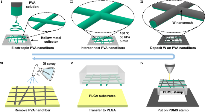
(I) Electrospinning PVA nanofibers on hollow metal collector (Al). (II) Interconnecting electrospun PVA nanofibers by heat pressing with a condition of 50 kPa at 180 °C for 5 min. (III) Depositing W on PVA nanofibers by magnetron sputtering. (IV) Putting W@PVA nanomesh on PDMS and laser-cutting unnecessary region such as metal collector. (V) Transferring W@PVA nanomesh to PLGA substrate using PDMS stamp. (VI) Removing PVA nanofibers by spraying DIW.
Figure 3a showcases the transparency of W/PLGAs with various electrospinning times placed above white paper. Figure 3b shows the morphology of random networked and continuously interconnected W nanomesh through PVA nanofiber welding process while Supplementary Fig. 8 exhibited the disconnection of W nanomesh on non-welded PVA nanofibers. Figure 3c shows the transmittance profile of W/PLGA with different electrospinning times. Transmittance at 550 nm decreased to ~92.4%, ~74.6%, and ~49.3% as the electrospinning time increased to 30 s, 45 s, and 75 s, respectively. Figure 3d shows a trade-off behavior between conductivity and transmittance. The sheet resistance, which is proportional to inverse of conductivity, decreased to 2663.5 Ω sq–1, 892 Ω sq–1, and 415 Ω sq–1, with a decrease in the transmittance. The PVA nanofiber density increases with higher electrospinning time, leading to decreasing transmittance by lowering voids for light transmission while forming more conductive networks of W nanomesh. The optical and electrical properties of the W/PLGA can be tuned by adjusting the electrospinning time according to the desired purpose. The sheet resistance effect on the electrochromic properties of WO3 for BECD utilization was evaluated using various sheet resistances of ITO. A minor difference in the contrast ratio (~56% to ~54%) and response time (tc ~9.12 s to ~32.01 s; tb ~ 19.19 s to ~34.42 s) was noted when the sheet resistance increased from 20 Ω sq−1 to 1 kΩ sq−1 (Supplementary Fig. 9). The electrospinning time of W/PLGA was adjusted by prioritizing the initial transparency of W/PLGA over the response time aiming for a large contrast ratio for BECD operation. W/PLGA electrodes fabricated with a 45 s electrospinning time were utilized for BECD and related applications.
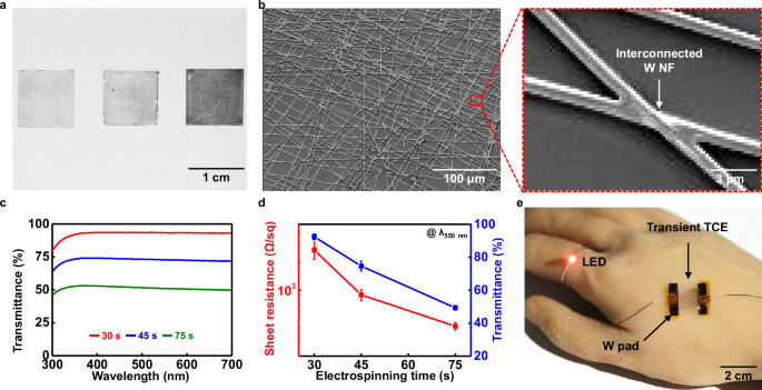
a Photographic images of the W/PLGA with 30 s (left), 45 s (middle), and 75 s (right) of electrospinning time (Aperture F 5.6 and ISO 1600). b SEM images of W nanomesh transferred on PLGA substrate (left). Magnified view of an interconnected junction in W nanomesh (right). c Transmittance spectra from 300 to 700 nm wavelength and (d) correlation between sheet resistance and optical transmission at 550 nm wavelength of the W/PLGAs with different electrospinning times (A, 30 s ; B, 45 s ; C, 75 s) (n = 4). e Photographic images of the LED operation connected to W/PLGA bent on an artificial hand with external voltage 3 V (Aperture F 4.0 and ISO 6400).
Figure 3e demonstrates the usability of the W/PLGA with ~75% transparency on human-like artificial hand by showing the operation of red LED on bending deformation. The W/PLGA provided showed good performance when bent along a curvature of human hand, as evidenced by the well lighting LED connected with a commercial 3 V Li ion battery. The flexibility of the W/PLGA can be attributed to the low bending stiffness of the metal nanofibers which have a line width of less than 1 μm. Supplementary Fig. 10 shows resistance change at various bending radius. Resistance increased by less than double up to a curvature radius of 15 mm, but gradually increased on smaller radius curvature.
Electrochromic performance of the BECD and its biodegradation
Figure 4 illustrates the structure and performance of the BECD. It consists of not only degradable electrochromic layer, electrolyte, but also degradable transparent conductive film, and shows electrochromic performance compared to previous studies (Table 1). The BECD is composed of fully biodegradable TCE (1 μm radius of W nanomesh on PLGA 50 μm thick), electrochromic layers (WO3 100 nm thick), and solid-state electrolyte (sodium chloride (NaCl) 1 M and Na4Fe(CN)6 0.1 M agarose hydrogel 1 mm thick) (Fig. 4a) sealed by encapsulation well (polyanhydride polymer (PA23) 1 mm thick).
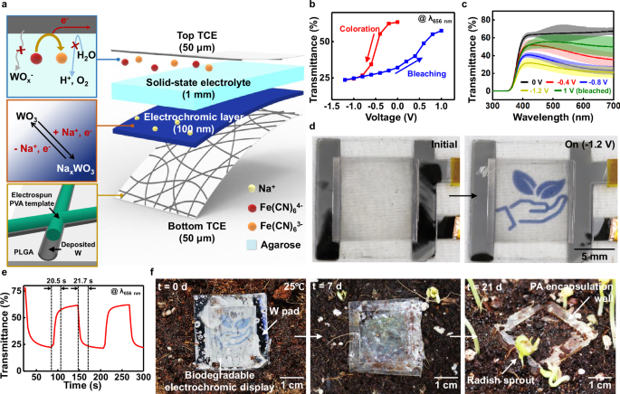
a An exploded view of the BECD. The BECD is composed of a TCE made of W nanomesh deposited on electrospun PVA template followed by transferring to PLGA, an electrochromic layer made of WO3 which exhibited a color transition from transparent to deep blue through a Na+ ion intercalation, and a solid-electrolyte made of NaCl 1 M agarose hydrogel with Na4Fe(CN)6 that lowers the operating voltage and reduces side reactions. b Transmittance change of the BECD at 656 nm wavelength during sweeping potential from 0 V to –1.2 V (coloration, red) and from –1.2 V to 1 V (bleaching, blue). c Transmittance spectra in range of 300 to 700 nm wavelength of the BECD with applied voltage of 0 V (black), –0.4 V (red), -0.8 V (blue), -1.2 V (yellow), and 1 V (green). Vivid and thick colored lines are average data, and pale colored area is standard deviation data (n = 4). d Photographic images at on/off states of the BECD on white paper (left is an initial state and right is on state which applying –1.2 V) (Aperture F 5.6 and ISO 1600). e Response time of the BECD measured during cyclic on/off states (–1.2 V/ 1 V). The left dashed line region is bleaching time (tb = 20.5 s) and right dashed line region is coloration time (tc = 21.7 s). f Sequential images of degradation of the BECD on a soil with radish seeds planted and sprinkled water every day for 21 days at room temperature (Aperture F 5.6 and ISO 6400).
Figure 4b shows the changes in transmittance at 656 nm wavelength of the BECD with applying negative voltage sweep from 0 V to –1.2 V and positive voltage sweep from –1.2 V to 1.0 V. During the negative voltage sweep, transmittance decreased rapidly to ~26.7% at –0.8 V, and subsequently stabilized to ~23.7% at –1.2 V. In the positive voltage sweep, transmittance increased slowly to ~32.1% at 0 V and rapidly to ~55.1% at 0.8 V, and then eventually stabilized to ~57.5% at 1 V. On/Off (coloration/bleaching) states with reduced water decomposition can be determined as –1.2 V and 1 V, respectively. Figure 4c illustrates the corresponding transmittance spectra of the BECD when various potentials were applied, depicting the average values within the standard deviation range. Transmittance at visible spectra (400–700 nm) was ~66.7% at initial state (0 V). It decreased gradually as –0.4 V was applied to the WO3 layer, ultimately changing to ~21.6% at the on state (–1.2 V), resulting in deep blue coloration by absorbing a greater portion of the light above a 500 nm wavelength. Then, it recovered to ~50.9% at the off state (1 V). The contrast ratio at wavelength 656 nm (Δ%T656) was ~45.1% at 1st coloration and ~29.3% at subsequent coloration, and the integrated contrast ratio (Δ%Tint (400–700 nm)) was ~39.5% at 1st coloration and ~27.3% at subsequent coloration. Figure 4d and Supplementary Fig. 11 display a series of the BECD images with ‘plant on hands’ icons at on/off state achieved by applying -1.2 V and 1 V, respectively. The deep blue color observed at on state confirms the electrochromic effect of WO3 with reduced water decomposition, and the BECD became transparent again by applying 1 V for transition to off state as shown in Supplementary Fig. 11. Figure 4e describes switching times during on/off cycle measured by the changes in transmittance at 656 nm wavelength. The tc and tb were 21.7 s and 20.5 s respectively, showing the comparable results to a previous electrochromic device of sputtered WO3 on ITO electrode56. While the transmittance at initial state was ~77.8%, there existed a little difference with the transmittance at bleached state, which stood at ~61.6%. This is because the sputtered WO3 layer was an amorphous state with a disordered arrangement of the WO6 octahedron structure and was distorted through the electrochromic reaction leading to a loss of structure (Supplementary Fig. 12)57. The intercalated ions trapped in deep sites of WO3 were hard to deintercalate during the bleaching process, so they failed to reach the transmittance at initial state. Although a similar level of transmittance was maintained in subsequent cycles, the response time increased and the contrast ratio decreased after a few cycles due to the gradual degradation of W and WO3 within the aqueous electrolyte (Supplementary Fig. 13). The calculated coloration efficiency, which is the optical density change according to the charge density, at 1st coloration (η1st) was 40.63 (pm) 2.41 cm² C−1 and at subsequent coloration (ηgen) was 32.42 (pm) 2.04 cm² C−1 (Supplementary Fig. 14). Contrast ratio decreased after 1st coloration due to irreversibly non-bleached region, but the remaining region showed well electrochromic reaction at subsequent coloration.
All the components of the BECD eco-friendly degrade into ions, hydroxides and/or monomers by water and/or enzymes, and their degradation products are biocompatible58,59,60,61. W and WO3 degrades by following reaction52:
PLGA and PA degrade through the cleavage of ester bonds caused by hydrolysis, and agarose degradation occurs through the cleavage of glycosidic bonds catalyzed by microorganisms abundant in soil62,63,64. A degradation test of BECD following the ISO 14855 standard, which serves as an assessment metric for the extent of degradation in a typical terrestrial soil environment, was conducted. A disintegration of BECD occurs within 49 days that size of residue was reduced more than 90% (Supplementary Fig. 15). Figure 4f showcases the degradation behavior of the BECD in soil with radish seeds planted. The degradation process began with the formation of cracks or wrinkles on the PLGA substrate followed by the degradation of the agarose electrolyte. After 21 days, all parts except the PA encapsulation well almost degraded, and the radish seeds planted around the BECD had sprouted and grown verifying the eco-friendly degradation. Furthermore, an acceleration test was conducted for PA degradation in a sodium hydroxide (NaOH) 1% PBS solution at 37°C showing total degradation in 7 h (Supplementary Fig. 16).
Demonstration of patternable BECD
Figure 5 shows the application of the patternable BECD in multiplication of pixels and integration of electrochemical devices using ~75% transparency of W/PLGA. Figure 5a shows the structure of a digital font-like BECD composed of 7 discrete pixels (hexagons with 5 mm long and 2 mm wide) through patterning the W nanomesh and WO3 layer using a laser cutter and depositing via stencil mask, respectively. Figure 5b showcases various letters ‘S’, ‘N’, and ‘U’ by applying voltage to desired pixel combinations. Each pixel was connected to an independent power supply and the characters were formed by applying –1.2 V to appropriate pixels.
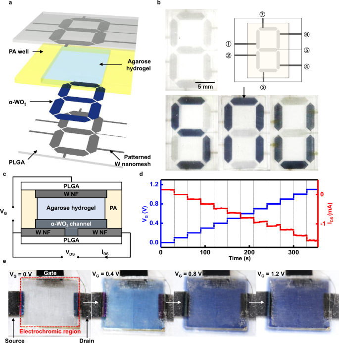
BECD was fabricated by utilizing 45 s electrospun W/PLGA (~75%T and ~890 Ω sq−1). a Schematic illustration and (b) photographic images of a digital font-like BECD. Characters ‘S’, ‘N’, ‘U’ have shown by applying –1.2 V to appropriate pixels for each character, such as pixel number 1, 3, 4, 5, 7 for character ‘S’ (Aperture F 5.6 and ISO 1600). c Schematic illustration of biodegradable electrochemical transistor integrated with electrochromic layer. d Gradual increase of drain-source current by elevating gate voltage 0.1 V per 30 s. e Gradual color change of the biodegradable electrochemical transistor with increasing channel conductivity by applying 0 V, 0.4 V, 0.8 V and 1.2 V to gate electrode (Aperture F 5.6 and ISO 1600).
The BECD enables the visualization of the operation of biodegradable electrochemical device such as a biosensor or an electrochemical resistive switching devices (ECRAM) through simple integration. Figure 5c illustrates a schematic of the three-terminal ECRAM which modulates a conductance of the channel in response to the voltage applied across the gate utilizing WO3 electrochromic layer of the BECD. ECRAM composed of source and drain electrodes (W nanomesh, 1 μm radius), channel (WO3 film, 100 nm thick and 100 μm width, Supplementary Fig. 17), electrolyte (NaCl 1 M and Na4Fe(CN)6 0.1 M agarose hydrogel, 1 mm thick) encapsulated with PA well, and the gate electrode (W/PLGA, ~50 μm thick) exhibited changes in electrical conductivity via doping through cation intercalation65. Figure 5d shows the current change between source and drain (IDS) upon applying voltage to gate electrode (VG) from 0 V to 1.2 V in increments of 0.1 V. Under a voltage between source and drain (VDS) of 0.1 V, IDS exhibited a steep increment up to -0.157 ± 0.019 mA, indicating that it changes memory state based on VG by modulating the conductance of WO3 channel layer via the extent of Na+ intercalation. IDS also maintained under same VG indicating the storage of information in the form of ion doping states. Figure 5e shows the color change of the device at 0 V, 0.4 V, 0.8 V, and 1.2 V of VG. As VG increased, the device underwent a color change from transparent to deep blue, thereby facilitating visualization of each memory state based on the resultant color change.
Demonstration of simple integration capability with biodegradable UV detecting sensor
Figure 6 shows the application of visualizing the detection of UV irradiation which can cause skin aging and cancer by easily integrating with BECD. Figure 6a, b shows the configuration of a biodegradable UV sensor integrated with BECD and a biodegradable battery, where all the components were composed of biodegradable materials. The biodegradable UV sensor was composed of UV detecting layer (AZO nanoparticles/PCL/TG paste, 140 μm thick) on Mo electrode (Mo nanoparticles/PBAT paste, 140 μm thick) (Supplementary Fig. 18). The sensor exhibited a reduction in resistance from 3 MΩ to 1.6 kΩ by UV irradiation of 15 W power at a distance of 30 cm (Fig. 6c). The biodegradable battery, composed of a MoO3 cathode (MoO3 nanoparticles/PCL paste, 280 μm thick), a Mg anode (Mg foil, 100 μm thick), and an electrolyte (NaCl 1 M agarose hydrogel, 1 mm thick) (Supplementary Fig. 19), maintained a stable voltage of ~1.5 V at 0.01 mA cm–2 discharging current, and gradually decreased to around 1 V at 0.1 mA cm−2 (Supplementary Fig. 20). Figure 6b illustrates a schematic circuit diagram showing series connection of the BECD and the UV sensor. Applied voltage of the BECD increased by decrease in resistance of the UV sensor, leading to an electrochromic response. Figure 6c shows the change in voltage applied to the BECD in response to the resistance of the UV sensor by UV irradiation. In the absence of UV irradiation, resistance of the UV sensor was ~3 MΩ resulting in nearly 0 V applied to the BECD. However, the resistance of the UV sensor rapidly decreased to 1.6 kΩ which leads to an increase in voltage applied to the BECD up to 1.2 V under UV irradiation. Figure 6d displays series of the BECD images with ‘UV CAUTION’ icons with UV irradiation. Figure 6e and Supplementary Figure 21 showcase the degradation behavior of the BECD integrated UV sensor in pH 7.4 PBS solution at 37°C. The BECD and Mg foil of the battery began to degrade initially, and almost degraded after 28 days. Subsequently, the Mo foil, UV sensor, and MoO3 cathode paste of the battery degraded sequentially under accelerated conditions of pH 8 PBS solution at 50 °C after 28 days to 98 days.
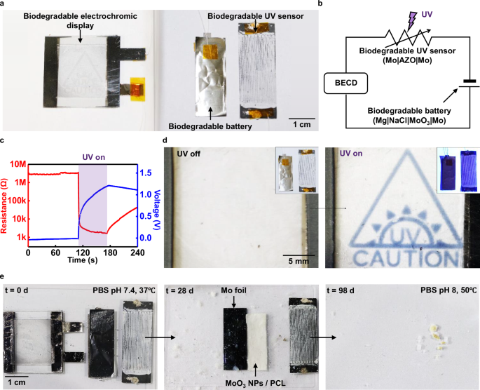
BECD was fabricated by utilizing 45 s electrospun W/PLGA (~75%T and ~ 890 Ω sq−1). a Photographic images (Aperture F 5.6 and ISO 1600) and (b) schematic circuit illustration of the BECD integrated biodegradable UV sensor and battery. Biodegradable UV sensor is composed of Mo/PBAT electrode and AZO/PCL/TG UV sensitive layer. Biodegradable battery is composed of MoO3/PCL on Mo cathode, Mg anode and NaCl 1 M agarose hydrogel. c Resistance change of biodegradable UV sensor and applied voltage change of the BECD with UV irradiation. d Photographic images of the BECD without (left) and with (right) UV irradiation (Aperture F 5.6 and ISO 1600). e Sequential images of degradation of the BECD integrated biodegradable UV sensor and battery with the condition PBS pH 7.4 at 37 °C up to 28 days, and PBS pH 8 at 50 °C up to 98 days (Aperture F 5.6 and ISO 1600).
Discussion
In summary, we develop a disposable BECD that all constituent compositions degrade environmentally friendly. A ~75%T transparent biodegradable TCE with a sheet resistance of ~890 Ω sq–1 was achieved by interconnected nanomesh structure of deposited W on PVA nanofiber template via electrospinning which was transferred onto PLGA substrate. Adding Fe(CN)64− ions to the electrolytes enhanced the stability of the BECD operation by reducing the operating voltage and mitigating corrosion of the TCE. Patternable capability of the BECD enables to form the multiple pixels tha simply shows diverse and complex image implementations. Visualizing biodegradable ECRAM and UV sensor through simple integration with BECD demonstrates the potential application for displaying various electrical, optical, and electrochemical signals of disposable electronics such as patches, sensors, and wearable devices in a closed-loop system.


Responses