Fully screen printed stretchable liquid metal multilayer circuits using green solvents and scalable water-spray sintering

Introduction
Soft and stretchable electronics provide unique opportunities for wearable and biomedical applications such as skin electronics1,2, implantable electronics3,4,5, smart wearable devices6,7, and soft robotics8. The combination of softness and stretchability allows for the seamless interfacing of curved and deforming systems beyond the capabilities of conventional rigid and flexible electronics. Recently, gallium (Ga) based room-temperature liquid conductors9,10 have received major attention based on their unique combination of fluidity and conductivity11,12,13. Liquid metals (LM) based on Ga have low toxicity12,13 and near zero vapor pressure11, making them promising for high-volume manufacturing and printed electronics. Ga-based alloys have high surface tension (≈600 mN/m) and spontaneously form a passivating oxide layer in air14. The oxide layer lowers the surface tension and helps to maintain the shape of the liquid. Although the oxide layer reduces the conductivity, its ability to adhere to many surfaces has been utilized in the development of patterning methods for Ga alloys14. Bulk Ga alloys can easily be patterned by microfluidic injection molding15, surface wetting16,17, and direct writing18. For large-scale printing of circuits, one promising approach is to disperse bulk liquid metal into droplets in an ink, which allows for control of the rheology and wetting of the ink. Liquid metal particle-based inks can be used with a variety of printing techniques, including stencil, stamp, and screen printing19,20,21,22. The inks are typically formed by sonicating Ga alloy in a polymer solution to form a dispersion of liquid metal droplets. As an insulating native oxide layer forms around the particles in the process, good electrical conductivity can only be achieved by sintering the particles in the printed layer.
To merge the particles, the oxide skin must be broken, which can be achieved by mechanical or chemical means. Mechanical sintering is achieved by applying forces in various ways9,23,24 to the oxide skin, which can break at a surface stress above 500-600 mN/m14. Chemical sintering is typically performed by exposure to chemical solutions or vapors such as strong acids or bases25,26 to remove the oxide layer around the liquid metal particles. The feasibility of the sintering method depends on the ink composition and the materials in the printed stack. Mechanical treatment is a common way of sintering the particles. Stretching23 can break the oxide layer and induce sintering but is impractical to incorporate into a fabrication process. Sonication9,27 is an alternative method, that can produce promising results, but optimal performance requires submersion in a media. Sonication can also be performed from the bottom of the substrate, but then results in inferior conductivity. Sintering can also be accomplished by thermal treatment, e.g. through laser sintering28 or photonic sintering29. The reported laser sintering method is serial in nature28 and would require substantial investments to transform into a large-scale production method. Photonic sintering29 using a flashlight will consume less energy than laser sintering, but the process has only been demonstrated for heat-resistant non-stretchable substrates. Chemical sintering relies on post-treatments to remove the oxide skin of the particles, which typically require the vapor, or solution, of a strong acid or base25,26. Such methods can be difficult to control, and safety issues make them less attractive for high-volume manufacturing. Hydrogen doping30 of the insulating oxide layer is another way of inducing sintering without removing the oxide skin, but the process involves harmful solutions and an annealing process. Other methods like capillary force31 and acetic acid-assisted32 self-sintering after deposition are difficult to integrate with screen printing on a large-scale.
Here, we report on a scalable approach for screen printing of multilayer stretchable liquid metal circuits using green solvents. The developed ink is composed of liquid metal particles dispersed in the ecofriendly solvent propylene glycol (PG) and the harmless dispersing agent polyvinylpyrrolidone (PVP). Screen printing is used in combination with automated water-spray sintering to achieve conductivities up to 7.3 × 10⁵ S/m. Optimal sintering was achieved by optimizing both ink composition and the water-spraying parameters. The printed circuits showed high stretchability (>800%) and excellent cycling stability (>500 cycles). Interestingly, the conductor morphology gives a resistance increase of less than 10% during 50% strain cycling, which is far below the expected 125% increase due to the geometry factor. Multilayer circuits were achieved by incorporating screen-printed insulating layers of thermoplastic polyurethane (TPU). The capability of the method was demonstrated by printing stretchable near-field communication (NFC) circuits that could be read out by a mobile phone. Altogether, the developed method shows great promise for scalable manufacturing of stretchable electronic circuits in an industrial setting.
Results and discussion
Printing process
The scalable fabrication process, including ink formulation, screen printing, and sintering, is illustrated in Fig. 1. The ink is formed by dispersing liquid eutectic gallium indium (EGaIn, melting point 15.7 °C) into a solvent by tip sonication. The use of a green and harmless solvent is important to enable scalable production in an open printing environment. The solvent PG was, therefore, chosen as it is widely used in edible items and in pharmaceuticals. PG also has a rather high boiling point of 188.2 °C, which is suitable for screen printing to avoid spontaneous drying in the screen. PVP was chosen as a combined dispersion agent and rheology modifier due to its safety, as it is a common pharmaceutical additive. The ink showed a shear thinning behavior, starting at a shear viscosity of 27 Pa·s at 0.1 s−1 shear rate, followed by a gradual decrease to 2.5 Pa·s at 1000 s−1, which is a suitable viscosity range for screen printing (Supplementary Fig. 1a). The ink produced good printing quality in a semi-automatic screen printer (EKRA E2) when printed on stretchable commercial TPU substrates (Supplementary Fig. 2). After drying, the printed layers were nonconductive due to the electrically insulating oxide layer around the EGaIn particles, thus a sintering step was needed. To allow for industrial manufacturing, the sintering method needs to i) be applicable to large-area surfaces, ii) be compatible with common substrates and printing materials, iii) use harmless chemicals, iv) allow high-throughput, v) keep registration throughout the process (e.g., no deformation of the substrate). To fulfill these requirements, we developed a sintering method based on water spraying by using a programmable spray coater allowing substrate sizes up to A3. The sprayer includes an airbrush that generates microdroplets which are spread over the heated substrate according to a program. The liquid metal particles in the dried ink are covered by a PVP layer (Fig. 1e–i), which is sensitive to humidity. The sprayed water causes the PVP layer to swell (Fig. 1e–ii) and subsequently shrink when dried. The induced mechanical forces in this process cause the oxide layer of the particles to locally break and thereby merge the particles together (Fig. 1e–iii). After several swelling and drying cycles, the previously isolated particles have then merged into a continuous conductive network which causes the conductivity of the printed layers to increase dramatically.

a The ink is produced by dispersing EGaIn into a PG-PVP solution through tip sonication. The EGaIn dispersion is stable due to the adsorbed PVP on the oxide surface. b The ink is screen printed by a conventional printer on the substrate. c After printing and drying, the print is made conductive through water-spray sintering that merges the EGaIn droplets. d Spray sintering is performed on a hotplate with a spraying robot scanning over the substrate. e Repeated cycles of swelling and drying of the PVP layer within the print create internal strain, which causes mechanical sintering of the particles.
Water-spray sintering
The spraying process needs to be carefully controlled to guarantee uniform sintering over large areas. The aim is thus to uniformly spread water droplets over the printed patterns. The key parameters (height, velocity, pitch) of the spraying process are illustrated in Fig. 2a where a specific spray head (airbrush) is used to generate a fixed spray flow. The maximum settings for height (80 mm) and pressure (2 bar, fully open valve) were used to maximize the coverage of a single spraying pass. For characterization of the water deposition density, water with added blue dye was sprayed on A4 white papers (Supplementary Fig. 3a, b). The generated blue traces on the papers were scanned, and the color density was analyzed using an image processing program (ImageJ, Supplementary Figs. 3c and 4). As expected, the water density depended strongly on the spraying velocity (Fig. 2b), with the amount of sprayed water following the expected theoretical trend (Supplementary Fig. 5). The bell-shaped distribution curve confirmed that the sprayed water density was highest in the center and decreased towards the edges. We thereafter investigated how the distance between the spraying scans, or the spraying pitch, influenced the water density distribution curve, and found that 10 mm pitch produced a uniform water distribution (Fig. 2c). For larger pitch values, the contributions from the individual traces can be seen as waves in the water density profile. For smaller pitch values, the distribution of water will be concentrated due to the stacking of individual traces. To verify that these results translated into uniform sintering, printed lines were placed at different positions and orientations with respect to the sprayed area (Fig. 2d). The blue arrows indicate the spraying directions, the red lines represent the distribution of water, the black patterns show the placement of printed lines and blue rectangles are the sprayed area. The measured conductivities for the various positions and orientations within the sprayed area (positions 1, 3, 4) had a narrow distribution, while samples placed on the border of the sprayed area had a slightly larger variation (position 2). We could thus conclude that 10 mm pitch produces a homogeneous sintering result over a large area. Each water-spraying cycle was programmed to cover the whole area of the printed pattern, which typically resulted in multiple spraying sweeps (Fig. 2a). As the sprayed area dried within 2 s due to the heating by the hotplate underneath, there was no need for introducing any waiting time in between cycles.
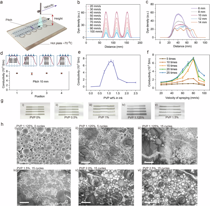
a Illustration of the parameters of the spraying process. b Sprayed water density as a function of spraying velocity. c Optimization of spraying pitch for 80 mm/s spray velocity. A pitch of 10 mm provides uniform coverage without extensive overlap. d Sintering uniformity for printed conductors at different locations with respect to the sprayed area. e Optimization of the PVP content of the ink with respect to final conductivity. f Sintering efficiency as a function of spraying velocity and number of cycles. g Photographs of sintered printed conductor with different PVP content. h SEM images of printed conductors before and after sintering for various conditions (all scale bars: 5 µm).
As PVP both facilitates the sintering of the particles but also may act as an insulating matrix within the prints, we expected the PVP concentration to heavily influence the results. Indeed, the achieved conductivity varied greatly with the PVP concentration in the ink, reaching a highest conductivity of 7.32 ± 0.30 x 10⁵ S/m for 1.125 wt% PVP (Fig. 2e). Low PVP concentrations proved insufficient to induce the necessary sintering, while high PVP concentrations also reduced the conductivity, likely due to its insulating effect. The macroscopic effect of the PVP concentration on the sintering can be seen in photographs, where the film morphology changes during sintering at higher PVP concentrations but not at lower ones (Fig. 2g).
The degree of sintering also depended strongly on the number of applied spraying cycles and the spraying velocity (Fig. 2f). The hotplate heating ensured that the prints dried in between each spraying passage. The degree of sintering improved with the number of applied spraying cycles until it saturated at around 20 cycles. This was rather expected, as repeated shrinking cycles can rupture and merge more and more of the particles. Fully sintered traces (Supplementary Fig. 6c) have a rougher and shinier look than the non-sintered ones (Supplementary Fig. 6a) and partly sintered samples (Supplementary Fig. 6b). Interestingly, the same monotonic trend cannot be seen for the spraying velocity, which shows a distinct optimum at 80 mm/s. That sintering is inefficient at too high velocities (>80 mm/s) with too little water is quite natural, however the characterization also reveals that too much water (<80 mm/s) can be as detrimental. One hypothesis could be that it is desirable to swell the PVP in place to induce strong shrinkage forces upon drying while flooding the print with water could mobilize the PVP phase and potentially separate it from the particles. Lower spraying velocities created larger water droplets on the surface of the prints, causing uneven water distribution, flowing of particles, and coffee ring effects (Supplementary Fig. 7). For the optimum spraying condition, a water layer of 8 µm average thickness was deposited (calculated from Supplementary Fig. 5 and the spraying pitch), which is similar to the thickness of the printed conductor layer. This small amount of water did not distort the shape of the printed pattern (Supplementary Fig. 8, 9). SEM images of various sintering conductions can provide further insights into the process (Fig. 2h). Figure 2hi-iii shows how particles merge into larger ones with increasing number of sintering cycles (0, 5, 15 cycles). At 15 cycles, for which the conductivity has saturated, most particles have merged into large domains which facilitates the macroscopic conduction. When increasing the PVP concentration beyond the optimal condition (>1.125 wt%, Fig. 2h iv–vi), the merging of large particles is quenched, which explains why the conductivity saturates at a much lower level. Multilayer stacks of conductors could be printed, with total thicknesses of 8, 16, and 22 µm for 1, 2, and 3 layers, respectively (Supplementary Fig. 10a). The efficiency of the sintering remained good, although there was a slight decrease in conductivity for multilayers (Supplementary Fig. 10b). The ink showed excellent storage stability, with stable performance of printed layers for up to 8 months storage time (Supplementary Fig. 1b).
Conductor performance under strain
Next, the electrical performance under strain was evaluated for printed conductors with a printed TPU encapsulation layer on top. The prints showed good quality and line widths down to 200 µm were easily reproduced (Fig. 3a, Supplementary Fig. 8). As the filler particle size was ≤5 µm (Fig. 2h), a finer screen mesh in combination with optimized printing parameters should allow for a substantial reduction in line widths if needed. Printed conductors of different line widths showed similarly good performance under strain and remained highly conductive up to about 800% strain at which the substrates fractured (Fig. 3b). Furthermore, the test samples also demonstrated excellent performance for strain cycling up to 200% strain by maintaining a relative resistance change below a factor of 2 (Fig. 3c). Stress-strain measurements showed increasing elongation of the samples with strain (Supplementary Fig. 11), which explains why the resistance does not fully recover in the relaxed state after higher strains. The strain rate had no major effect on the electrical performance (Fig. 3d). During 500 strain cycles at 50% strain, the relative resistance change stabilized well below a 10% increase of the original resistance (Fig. 3e), which is surprisingly good considering the geometrical change of the conductor during stretching. Altogether, the electrical performance under strain is excellent for the printed conductors, with a very low strain sensitivity.
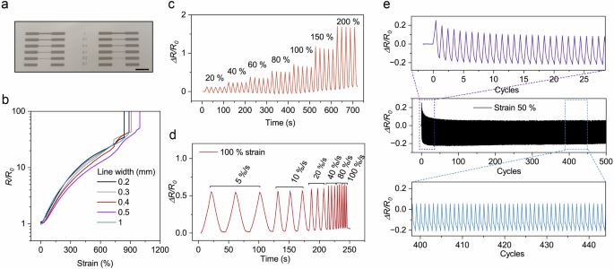
a Printed test structures with line widths varying from 0.2 to 1 mm. (scale bar 1 cm). b Relative resistance vs strain until break for different line widths. c Resistance vs strain cycles for increasing strain. d) Resistance vs strain cycles at different strain rates. e Strain cycling at 50% strain for 500 cycles.
Two aspects of the resistance-strain data deserve further attention and analysis; the decrease in resistance during strain cycling at moderate strain (Fig. 4b, dashed purple line), and the surprisingly small increase in resistance during stretching at higher strain (Fig. 4b, dashed red line). The first effect is known from literature as strain-induced sintering of particles23. After the water-spray sintering, most of the liquid metal particles are merged but there exist still some insulating domains within the film that can be broken by strain. The observed effect happens during the first strain cycles (Figs. 3e and 4b), which is consistent with the proposed mechanism (Fig. 4a). The result is that the resistance decreases when the printed conductor is exposed to moderate strain, which typically is beneficial.
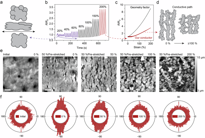
a Schematic illustration of strain-induced sintering in printed LM conductors. b Normalized resistance under strain cycling. The purple line indicates the region where the resistance decreases due to strain-induced sintering. The red line indicates the region where the resistance scales better with strain than the theoretical geometry factor. c Comparison of normalized resistance between the geometry factor ((1+ε)2, ε is strain) and our conductor. d Schematic illustration proposing the structural cause behind the better-than-theory performance. e Optical profilometer height maps of the printed conductor under strain (scale bar 0.1 mm). f Directionality of the conductive path based on 2D FFT analysis.
The second effect is less obvious, as it has been reported that liquid metal conductors maintain constant conductivity under strain33 and thus the resistance should follow the geometrical scaling ((1+ε)2, where ε is strain) of the conductor under strain34,35. As a conductor gets stretched, the cross-section area decreases, and the length increases (Supplementary Fig. 12), resulting in substantial increase in resistance even if the conductivity is preserved. For 200% strain, the geometry factor is (1 + 2)2 = 9, which implies that for preserved conductivity the resistance should increase with a factor of 9. In our case, however, the resistance only increases by a factor of 3.56 for our printed conductors (Fig. 4c). This implies that the conductivity of the conductors actually increases with strain and reaches an outstanding calculated value of 19 × 105 S/m at 200% strain. To understand this strain effect, we measured height maps using optical profilometry of the printed conductor at various strains (Fig. 4e). This revealed that our printed conductor does not behave like a pure liquid metal, as it is stiffened by integrated PVP domains. Prior to stretching, no major defects were visible in the film. After being pre-stretched to 50%, however, cracks perpendicular to the strain direction were visible. This is rather unfavorable for conduction, as the conductive path mainly goes perpendicular to the relevant direction. Upon stretching, the domains in the film tended to realign into a more random network, which is better for conduction. This was also confirmed by 2D fast Fourier transform (FFT) analysis of the height map, which clearly shows a realignment of the conductive domains in the strain direction (Fig. 4f, Supplementary Figs. 13 and 14). The suggested mechanism is illustrated in Fig. 4d, explaining how our conductor can scale better-than theory predicts by alignment of conductive domains. Similar behavior has been observed in conducting polymers, as the realignment of polymer chains/fibrillar domains can result in a conductivity increase for moderate strains36. One should note, however, that the liquid domains within the printed conductors have the possibility to flow within the PVP framework, making it different from just the realignment of fibrils. SEM images of stretched conductors indeed reveal that a liquid metal layer is formed in the cracks between the thicker and stiffer portions of the print (Supplementary Fig. 15). Upon release of the strain, a new texture is formed on the conductor, indicating remaining morphological changes that are consistent with an observed increase in conductivity. Together, the two described mechanisms can explain the principle behind the outstanding electrical performance of our printed conductors under deformation.
Printed stretchable NFC circuits
To demonstrate the capability of our developed ink and sintering process for large-scale manufacturing, the ink was printed in a semi-automatic screen printer EKRA (Supplementary Fig. 2a, b) within the manufacturing line at the Printed Electronics Arena facility in Norrköping. The prints showed good printing quality over the large-area substrates, onto which the developed sintering process could be applied without modification (Fig. 5a). The NFC circuit design (Fig. 5b) requires printing of several conducting and insulating layers on top of each other. Our process is compatible with this requirement, as vertical interconnect access (VIA) holes could be incorporated as openings in the printed insulating TPU layers, through which the conductor layers were interconnected (Supplementary Figs. 16 and 17). The overprinting compatibility of the liquid metal ink and the TPU ink thus allows for the fabrication of multilayer circuits, which enables the implementation of complex circuitry. The NFC antennas (Supplementary Fig. 18) were designed for an operating frequency of 13.5–14.0 MHz to meet practical use requirements. An NFC chip was mounted onto the antenna circuit to complete the NFC tag, which could be wirelessly read using a mobile phone (Fig. 5b). The printed antennas could be stretched, twisted, and heat-pressed onto textiles while maintaining their functionality (Fig. 5c, Supplementary Videos 1 and 2).
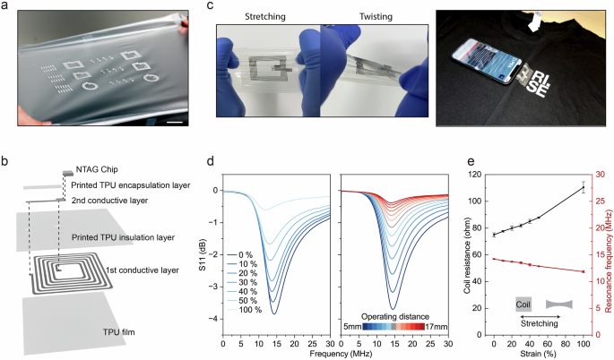
a Screen printed liquid metal pattern on a stretchable TPU substrate by a semi-automatic screen printer (scale bar 5 cm). b Exploded-view illustration of the layers in the stretchable NFC antenna. c The stretchable NFC circuits can be read out by a mobile phone when mounted on skin or on textile. d Scattering parameter S11 under uniaxial strain and different operating distances. e Resistance and resonance frequency of the coil under strain.
The reflection coefficient S11 is a key parameter for characterizing antennas for wireless radio frequency communication. The detecting circular single-turn loop antenna was placed in a customized plastic test fixture (Supplementary Fig. 19) to avoid metal interference. The manufactured NFC tags were tested under different strains and operating distances (Fig. 5d). Typically, the resonance frequency will decrease during stretching, as the increasing coil area results in higher inductance, which lowers the resonance frequency. As the size of the sensing loop is fixed, its matching to the stretched antenna worsens with strain, which causes a decay in signal strength (Fig. 5d, left). Similar decays in signal strength can be observed for increasing operating distances (Fig. 5d, right). The coil resistance increased a bit with strain, but no significant broadening of the resonance peak was observed (Fig. 5e). The resonance frequency remained within the intended range for up to 50% strain (Fig. 5e).
As the developed sintering technique here is inexpensive and harmless, it is interesting to consider how it could be scaled into a high-throughput setup. For both sheet-based and roll-to-roll processing, one can envision a station where the substrate is fed through multiple spraying units, where each unit has enough nozzles to cover the full width of the substrate. In such a setup, the drying time between spraying steps and the length of the station dictate the maximum feedthrough speed. For example, 15 spraying units with 2 s drying and a 2 m long station would give 4 m/min feedthrough, which is fast enough in the printed electronics context. It is challenging to compare our method to other previously reported sintering methods from a scalability perspective, as none of the methods have been upscaled to date. To give an indication, we have compiled the strengths and potential weaknesses of various liquid metal sintering methods in Supplementary Table 1 and conclude that water-spray sintering compares well to other potential methods with respect to upscaling. The use of inks with green solvents in combination with robust and scalable water-spray sintering makes the method attractive from a cost, safety, and performance perspective. We, therefore, believe that the reported method constitutes an attractive pathway toward high-throughput roll-to-roll manufacturing of printed stretchable electronics.
Methods
Dispersed liquid metal particle ink
Liquid metal EGaIn was made by melting Gallium (Gallant Metals, 99.99%) and Indium (Unique Metals, 99.99%) with a ratio (wt Ga:In 3:1) at 80 °C. The formulated ink contained liquid metal (EGaIn, Ga:In 3:1), PVP (Thermo Fisher Scientific Inc, MW 1,300,000), and (PG, MP Biomedicals). The ink solution was first prepared by dissolving PVP in PG (0, 2, 4, 4.5, 5, 6, 8, 10 wt% PVP in PG). The solution was stirred at 80 °C for 5 hours. Liquid metal was then added to the solution at a mass ratio of EGaIn:PVP-PG 3:1 and dispersed by tip-sonication (Fisherbrand FB-505, 5 seconds on, 5 seconds off, in total 1 min at 25% amplitude). The shear viscosity of the ink was characterized with a Malvern rheometer (Kinexus, Malvern Instrument Ltd). The viscosity was measured at an increasing shear rate from 0.1 s−1 to 1000 s−1 with a disposable plate (20 mm of diameter, Peltier disposable plate system, KNX 2155) and a parallel plate held at 25 °C.
Screen printing of liquid metal inks
Screens for printing custom-designed test structures were ordered from ACP Coated Screens Scandinavia AB, Sweden. TPU film (Platilon U073) purchased from Covestro was used as substrate. The screen printing of the liquid metal ink was conducted using an EKRA E2 semi-automated flatbed screen-printer. Exposed metal parts within the EKRA printer were covered with protective polyethylene foil to prevent corrosion with liquid metal. Additionally, the metallic filler in the EKRA printer was removed, and a wooden filler was instead used for manually refilling the mesh after the squeegee had returned to its initial position. 4 g of ink was sufficient for filling the screen for making multiple prints. The screens had a polyester mesh with a mesh count of 77 threads per cm and a thread diameter of 48 µm. The printing speed was 170 mm/s, and the printing pressure was 1.7 bar. After printing, the screen and the squeegee were vigorously cleaned with isopropanol and lab wipes. The prints were dried in an oven (Termaks TS 8056) at 80 °C for 10 min. The prints could also be dried in open air within 30 minutes.
Water-spray sintering
The water-spray sintering process was done using a programmable spray coater (TH-2004C) with an integrated hotplate from Tianhao Tech Inc. The position of the spray head (Airbrush BD-208 Nozzle diameter 0.2 mm) can be controlled in 3 dimensions. Fully dried printed substrates were fixed on a rigid plastic sheet and then placed on the hotplate at 70 °C. The pressure for the spraying was fixed at 2 bar. The spraying height was set to 80 mm, the maximum value, which yielded a covering width of 20 mm. The sprayer was programmed to have a scanning speed of 80 mm/s and a scanning pitch of 10 mm between the parallel scans (optimized setting). The scanning direction was the same for all scans. The spray coater was programmed to make sequential scans covering the whole area to be sintered. All the prints were sprayed at least 20 times unless otherwise stated.
Screen printing of multilayer circuits
A first conductive layer of liquid metal was screen printed on a TPU substrate and sintered by spraying water using the materials and methods described above. An insulating layer with VIA holes was thereafter formed on the first conductive layer by screen printing two consecutive layers of TPU using a screen with polyester mesh (21 threads per cm and 160 µm thread diameter) from ACP Coated Screens Scandinavia AB, Sweden. The transparent TPU ink was formulated based on a previously developed and reported ink (without the TiO2)37. The printed TPU layers were each cured in an oven at 100 °C for 2 min. A second conductive layer of liquid metal was printed on top of the insulating TPU layer followed by water-spray sintering. A final insulating layer of TPU was printed on top to encapsulate the device.
Optimization of water-spray sintering parameters
Water diluted with blue dye (Oetker Sverige AB, 5 ml dye in 30 ml DI water) was used for identifying optimum water-spraying process parameters. The dyed water was sprayed on white A4-sized paper substrates at scanning speeds of 20, 30, 40, 50, 60, 70, 80, 90, and 100 mm/s. The height of the sprayer was set to 80 mm (maximum value). The length of the spraying traces was 100 mm. Three traces were sprayed for each spraying velocity. The temperature was set up to 70 °C for the hotplate underneath. After completely drying the substrates after spraying, the sprayed patterns were optically scanned to obtain digitalized images for analysis. At a velocity of 80 mm/s, four spraying lines were sprayed for each pitch distance (6, 8, 10, 13, 14 mm). The image processing software ImageJ was used for analyzing the color density on all the papers.
Morphology characterization
The samples were analyzed with an optical 3D profilometer (PLu neox 3D, Sensofar) to determine the layer thickness and for observation of the morphology. All scanning electron microscope (SEM) images were taken by a Sigma 500 Gemini (Zeiss). Microscope images were taken with a Leica DM LM microscope accompanied by LAZ EZ software.
Electrical and electromechanical characterization
Printed test structures (10 × 1 mm rectangular lines) with additional 10 × 2 mm contact pads at each side (Fig. 2g) were prepared for each water-spray scanning speed (20, 30, 40, 50, 60, 70, 80, 90, 100 mm/s). For each speed, all the test structures were sprayed continuously for multiple cycles (5, 10, 15, 20, 25 times). For the sintering uniformity investigation, four printed test structures (10 mm × 1 mm) for each spraying position were placed at four different positions and were sprayed under 80 mm/s with a pitch of 10 mm. For conductivity measurements, the resistance was measured using a Keithley 2612B SourceMeter and a four-point probe with Au-coated pogo pins. Electromechanical properties were characterized by a motorized linear stage (X-LSQ300A-E01, Zaber) with integrated four-point probe resistance measurements (Keithley 2701 Ethernet). The contact pads of the printed test lines were designed to match the dimensions of this test setup.
Opto-mechanical characterization
Optical profilometer images were converted into gray scale, and 2-dimensional FFT was calculated with the software Gwyddion to highlight the periodicity of the major conductive pathways in the height maps. The directionality was calculated from the radial distribution of the FFT components by using the software Fiji ImageJ.
Fabrication of stretchable NFC tags
NFC antenna coils were printed with the optimized liquid metal ink using the multilayer circuit process described above. The printed coils were sintered by water-spraying at a scanning speed of 80 mm/s and using 20 spraying cycles. An insulating layer (two printed TPU layers) with VIA holes and a conducting bridge layer of liquid metal were thereafter printed and sintered to complete the antenna circuit. Thereafter, two TPU layers were screen printed for encapsulation. Finally, an NFC chip (NTAG 215 from NXP) was placed on the contact pads of the printed antenna to form an NFC tag.
Design and characterization of stretchable NFC tag
The NFC antenna was designed with parameters (6 turns, 0.6 mm line width, 0.4 mm line spacing, 3.5 mm outer diameter) based on the coil design guide from NXP (https://community.nxp.com/t5/NXP-Designs-Knowledge-Base). The frequency response of the NFC antenna was measured by a network analyzer (miniVNA pro2). A self-made circular sensing loop with a diameter of 30 mm was integrated into a plastic box (plastic thickness 5 mm) designed for radio frequency measurements. The NFC tag was attached to the bottom side of a plastic plate that was mounted on a digitalized height elevator stage (Digimatic Heightgage, Mitutoyo) to control the vertical distance between the NFC tag and the sensing loop. The practical function of the NFC tag was characterized by using an NFC-enabled mobile phone (iPhone 12). An NFC tag that was transferred onto a T-shirt using a heat press was also tested.


Responses