High-performance magnetostatic wave resonators based on deep anisotropic etching of gadolinium gallium garnet substrates
Main
The backbone of modern handheld wireless communication systems is radio-frequency (RF) front-ends that selectively transmit and receive signals of interest. Typically, the received RF signal is first filtered using a bandpass filter. This filter is a key component of the RF front-end because it affects most of the performance metrics, including nonlinearity, noise figure and transceiver power consumption. A typical filter for mobile applications is synthesized using microscale resonators. The filter metrics, such as pass-band insertion loss and fractional bandwidth, are limited by the quality factor (Q-factor) and coupling coefficient (({k}_{t}^{2})) of the resonators used in filter synthesis. The coefficient ({k}_{t}^{2}) provides the efficiency of energy conversion from electrical to another form of energy1. For instance, in acoustic resonators, ({k}_{t}^{2}) quantifies the efficiency of converting electrical energy into mechanical or acoustic energy. Similarly, for magnetostatic resonators, ({k}_{t}^{2}) represents the efficiency of converting electrical energy into magnetic energy.
Microscale resonators based on surface acoustic waves and bulk acoustic waves dominate the RF front-end market because of their high performance in the sub-6 GHz frequency range. The key advantage of acoustic resonators for mobile applications is the nature of acoustic waves. The wavelengths of acoustic waves are shorter than those of electromagnetic waves at the same frequency. This difference allows acoustic resonators to be much smaller and more compact compared with traditional electromagnetic-based components. Their compact size, combined with their ability to maintain high performance, makes acoustic resonators highly suitable for use in mobile communication systems in which space is at a premium and efficiency is crucial. Current efforts are focused on scaling acoustic resonators to high frequencies and maintaining the Q-factor and electromechanical coupling. Materials like lithium niobate and scandium-doped aluminium nitride are, in particular, being explored for their potential to create high-coupling acoustic resonators for such advanced applications2,3,4,5,6,7.
The Frequency Range 3 band (7.1–24.2 GHz) is of interest in mobile communications2, radar systems8 and satellite communications9. There is an emerging requirement for filters within this range to support a bandwidth of more than 400 MHz (ref. 10), with even higher demands for satellite communications. Acoustic technology is although at an early stage of development in terms of scaling and performance in this frequency range. Frequency scaling is being addressed through the use of periodically poled piezoelectric films5,11, hybrid acoustic modes2 and overmoded resonators12. Filters based on electromagnetic cavity resonance can provide high performance and can be tuned to the desired frequency13. However, their size is limited by the electromagnetic wavelength, which is impractical for mobile applications.
Magnetostatic waves (MSW) are a subset of spin waves (collective excitations of electron spins) in an ordered magnetic material14. Unlike electromagnetic and acoustic waves, MSW can have nonlinear dispersion. This allows the frequency of the MSW to be tuned without changing the dimensions of the resonators. Their wide frequency tuning is based on bias-dependent dispersion. The dispersion is nonlinear with the wavevector; therefore, the frequency can be tuned by changing the resonator dimensions, too. Yttrium iron garnet (YIG) is the preferred material for MSW resonators due to its low damping properties, and tunable filters based on YIG spheres are an established technology15.
Commercial YIG filters are fabricated by manually aligning coupling transducer loops around a YIG sphere16. This approach creates challenges in terms of scaling. Moreover, these filters are bulky and consume high power due to the large tuning current flowing through an electromagnet. Thin-film YIG technology offers the advantage of large-scale production and integration with permanent magnets to offer zero-quiescent-power tuning17. Such thin-film YIG filters also offer wide tunability, which allows them to cover a broader range of frequencies. This feature could reduce the number of individual filters needed in a system to span a wide frequency spectrum. This could, in turn, lead to a smaller footprint for RF front-ends, optimizing space and possibly reducing costs in systems in which compactness is crucial.
Single-crystal YIG can be grown on a lattice-matched substrate—gadolinium gallium garnet (GGG). This YIG-on-GGG (YoG) platform can be used to develop tunable resonators18,19, tunable bandstop filters20,21 and tunable bandpass filters17,22,23. The platform is also of interest in applications such as magnonics24 and quantum information processing25. However, microfabrication technologies for YoG remain limited. For example, current patterning techniques do not allow complex device structures such as through vias or top-bottom electrodes, which are ubiquitous in silicon-based materials platforms. Due to these fabrication challenges, most YoG devices have the same basic structure, in which a metallic transducer is patterned on top of a patterned YIG film. This top-electrode-only design limits the resonator coupling to less than 3%; correspondingly, the filter bandwidths are limited to less than 40 MHz. The resonator coupling is a strong function of the distribution of the RF magnetic field inside the YIG film. With current transducers, metallic transducers on top of the YIG film are used to generate the excitation RF field. The generated RF field weakly couples to the MSW resonance.
In this Article, we report high-performance MSW resonators created through the anisotropic etching of GGG substrates. The approach uses a transducer with a hairclip-like structure, which brings the transducer trace much closer to the ground plane. This results in a coupling of more than 8%, maintaining a good Q-factor in the 6–20 GHz frequency range. To do this, we develop a microfabrication methodology that involves thinning and deep etching (up to 100 μm) of the GGG substrate.
Hairclip YoG resonator
The resonator design utilizes—now commonly available—the YoG material platform. The design of the hairclip YoG (HYG) resonators is shown in Fig. 1a. The resonator has a hairclip-like inductor loop structure in which the narrow top transducer metal meets the wide ground plane at the bottom of the GGG substrate. The continuity of the top and bottom metals is facilitated through the via holes in the GGG substrate. The structure of the hairclip is realized by etching three holes in the GGG layer—two beneath the ground pads of the coplanar waveguide and one adjacent to the YIG. These holes are referred to as through GGG vias (TGVs) in this Article. The device structure is analogous to a grounded coplanar waveguide transitioning to a microstrip line26. The transducer dimensions are chosen to satisfy the 50 Ω matching conditions in the coplanar waveguide section of the device. The YIG dimensions and microstrip transducers are co-designed to optimize the coupling for a given background impedance. The relative width of the YIG and transducer affects the Q-factor, relative spurious mode level and coupling. Increasing the metal transducer’s relative coverage enhances coupling, lowers the Q-factor and improves the relative spurious mode level27. The thickness of GGG under the YIG layer (tggg) is <8 μm. The cross-sectional image (Fig. 1a) shows a 100-μm-thick GGG substrate on which the resonator was fabricated. The GGG layer is made transparent to show different etching features in the device. The sectional view also shows the deep-etched GGG layer under the YIG layer. A third view of the resonator with a hidden GGG layer clearly shows the hairclip structure with different TGVs. The hairclip configuration results in the YIG being enclosed in a wraparound metallic loop, with the close proximity of the ground plane to the top transducer. This leads to the high confinement of the RF magnetic field within the YIG region. The distance between the YIG and ground plane is decided by the remaining thickness of the GGG (tggg) after the etching step. Simulated magnetic-field distributions on a cross-sectional plane of the resonator for tggg values of 5 μm and 25 μm are shown in Fig. 2a,b, respectively. These field plots demonstrate that the magnetic field is more tightly confined within the YIG layer when the GGG thickness (tggg) is 5 μm. To provide additional clarity, the average magnetic field inside the YIG layer for varying tggg values is plotted in Fig. 2c. Additionally, Fig. 2 illustrates the simulated Q-factor and coupling as a function of tggg. As anticipated, the coupling decreases sharply as the GGG thickness under the YIG increases. To achieve meaningful improvements in coupling, the GGG thickness beneath the YIG should be less than 20 μm. The hairclip design supports the efficient excitation of magnetostatic forward volume waves when an out-of-plane biasing field is used14. We focus on magnetostatic forward volume waves in this Article because it is easier to design a magnetic biasing circuit for this configuration. Figure 1b shows an image of the HYG chip containing several HYG resonators. Individual devices on the microfabrication mask were designed to have different opening sizes of TGV etching. Different etch-window sizes result in variable thicknesses of GGG under the YIG. Different etching windows also result in the unsuccessful formation of TGVs on some devices. The unsuccessful via formation results in the formation of a capacitor, which results in a resonantly coupled HYG (RHYG) resonator, as described later.

a, Three-dimensional rendering images of the HYG resonator device showing different layers and their topologies. The cross-sectional image (seen from the side of the marked eye) shows a 100-μm-thick GGG substrate on which the resonator was fabricated. The thickness of GGG under the YIG layer is marked as tggg. The GGG layer is drawn transparent to show different etching features in the device. A third view, in which the GGG layer is hidden, clearly shows the ground plane and TGVs. b, Chip micrograph of the HYG resonator showing various resonators on a grid. The HYG chip is mounted on a piece of Si wafer for easy handling. c, Optical image of a hairclip device after successful fabrication showing different features as explained for the three-dimensional (3D) schematic. d, Optical image of a GGG sample with 90-μm-deep etching. The image shows the anisotropic etch profile of the GGG substrate.

a,b, Magnetic-field distribution (H field) with tggg = 5 μm (a) and tggg = 25 μm (b). We can see that there is higher confinement of the magnetic field in the YIG region for lower tggg. c, Average magnetic field inside the YIG thin film as a function of tggg. d, Effective coupling (({k}_{t}^{2})) and Q-factor as a function of tggg simulated with an internal magnetic field of 360 mT corresponding to MSW frequency near 10.2 GHz.
Source data
Performance of tunable HYG resonators
An image of the chip with a grid of several resonators is shown in Fig. 3a. In this section, we discuss the results from a device in which we have formed the inductor loop around the YIG resonator through the etched TGVs. A non-magnetic ground–signal–ground RF probe is used to measure the reflection parameters of the device. An out-of-plane static biasing field was applied to support magnetostatic forward volume waves in the YIG resonator. Figure 3b shows the measured impedance response of a single HYG resonator at various static bias fields from 300 mT to 900 mT.
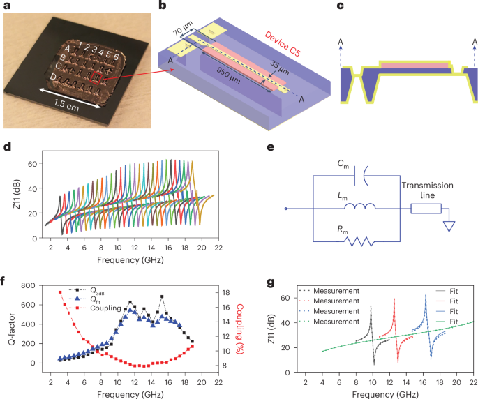
a, Photograph of the fabricated chip showing a grid of resonator devices. b,c, A 3D (b) and cross-sectional (c) schematic of the HYG resonator, showing the formation of the inductive loop around the YIG resonator. d, Frequency response of the HYG resonator at various bias fields (300 mT to 900 mT). e, Broadband equivalent circuit model of the HYG resonator showing a transmission line (representing the transducers) and a parallel RLC branch representing the MSWs. The circuit elements Cm, Lm and Rm represent equivalent capacitance, inductance and resistance of the magnetostatic branch, respectively. f, Frequency dependence of the effective coupling coefficient and Q-factor. g, Circuit-fitted impedance (Z11) response of the HYG resonator at different applied bias fields.
Source data
An equivalent circuit model for the MSW resonators has been presented in the literature28 and has been utilized by many researchers17,19,20. This circuit model consists of a series resistor (R0) and series indicator (L0) (representing the transducers) with a parallel RLC branch representing the MSW. This model works perfectly in a narrowband measurement. In this Article, the measurement results from a wide frequency range are reported. Hence, the lumped circuit model does not capture the behaviour of the device. A broadband circuit model of the resonator utilizing a transmission line is shown in Fig. 3e. In this model, the MSW is still modelled as a parallel RLC circuit; however, the transducer is modelled as a transmission line. The transmission-line model is first fitted to the zero-bias data of the resonator. When no bias is applied, the MSW does not exist in the resonator, and hence, the fitting parameters of the transmission line can be fixed for subsequent MSW fitting. Figure 3 shows the measured and fitted impedance responses at various bias fields for the combined M-line MSW response. The parameters of the M line are constant for fitting over different bias fields.
The performance metrics of the HYG resonator as a function of the resonance frequency are shown in Fig. 3d,f. From a filter design standpoint, the resonator Q-factor and coupling (({k}_{t}^{2})) are the two main metrics. For a low insertion loss and wideband filter, high Q and ({k}_{t}^{2}) are needed. The Q-factor of the device is calculated using the 3 dB bandwidth of the main peak, both from the raw measured data (Q3dB) and the circuit-fitted data (Qfit). The Q-factors obtained from both methods are shown in Fig. 3f. The effective coupling coefficient ({k}_{t}^{2}) was calculated using the expression (frac{pi }{2}frac{{f}_{p}}{{f}_{s}}times cot left(frac{pi }{2}frac{{f}_{p}}{{f}_{s}}right)), where fp and fs are the parallel and series resonance frequencies from the measured impedance response, respectively. The Q-factor of the MSW resonance increases with frequency up to a point (14 GHz) and then starts to decrease. By contrast, the resonator coupling initially decreases as we go higher in frequency. The initial coupling trend can be understood by the intuitive consideration that the equivalent inductance (Fig. 3e, Lm) representing the fact that the MSW resonance decreases as we tune it to a higher frequency. This behaviour is also expected from reported physics-based equivalent circuit models of spin waves28. The successive reduction in Lm results in progressively lower overall energy storage in the MSW resonance as we increase the frequency of MSW. The onset of coupling increase is not fully understood. One possible explanation could be the onset of spurious modes. It is likely that the spurious modes result in a higher coupling because of the presence of an additional parallel RLC branch. Although the initial increase in Q has been previously documented17,29, the underlying mechanisms driving this trend remain poorly understood. In particular, the sharp rise in Q beyond a certain frequency (9 GHz in this case) is a new observation. We suggest that losses in the MSW resonator require a dedicated, in-depth study to fully explain this behaviour. To understand the Q drop at higher frequencies, we characterize the transmission line in the absence of any external bias, thereby removing the MSW in the system. The losses in the transmission line (1 – ∣S11∣2) start to increase rapidly beyond 14 GHz (Supplementary Section 3.3), which could result in the loss of Q-factor. A comparison of performance metrics of the MSW resonators available in the literature is shown in Table 1.
RHYG resonators
The common techniques of MSW excitation utilize a broadband transducer, such as a coplanar waveguide or a microstrip line. A resonant coupling between the electromagnetic waves and MSW can also be achieved by bringing the electromagnetic resonance of the transducer and MSW resonance close to each other. Although this approach does not result in increased energy stored in the resonator, it can be utilized to increase the separation between fp and fs, thereby resulting in an increased fractional bandwidth of filters30,31. Here an external lumped element (inductor/capacitor) is utilized to match the electrical resonance closer to the main (acoustic/magnetic) resonance frequency. This matching can also be achieved using a transmission line27. Both these approaches incur size/area penalties to the device. The hairclip fabrication process, on the other hand, presents an opportunity to fabricate a capacitor between the top transducers and the bottom ground plane. Since the capacitor is formed in the thickness direction of the device, it avoids any area penalty. Because the etch rate of GGG depends on the size of the etch window, appropriate opening-window sizes can be chosen to get variable capacitors. We have variable sizes of etch windows in our layout design for backside GGG etching. The variable etch rate of GGG results in the non-completion of via etch in some devices (Fig. 4f, see Methods). The thickness of the remaining GGG layer determines the capacitance of the capacitor. The cross-sectional schematic of one such device is shown in Fig. 5c. When the MSW resonance is close to this LC resonance, a resonant coupling can be achieved. These devices are referred to as RHYG resonators in this Article.
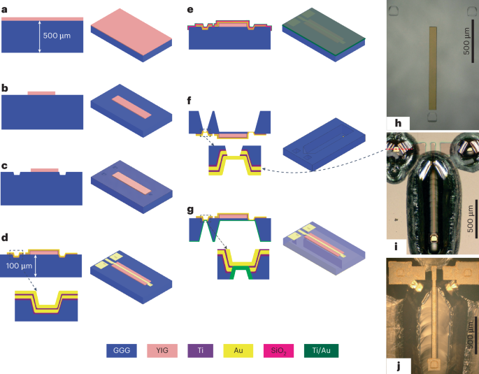
a, Starting YoG material stack. b, Patterning of the YIG layer using ion milling. c, Shallow (12 μm) etching of GGG from the top side using H3PO4 at 160 °C. An electroplated Au layer is used as a masking layer for the wet etching of GGG. An optical image of the sample after this step is shown in h. d, Patterned electroplating by using a Ti/Au/Ti/Au (10/150/25/150 nm) seed layer that was deposited using the GLAD method. e, Plasma-enhanced chemical vapour deposition of SiO2 and GLAD of Ti/Au, which is subsequently used as a seed to electroplate gold as a protection layer for the next processing steps. f, Backside deep etching of GGG using the same process as that in c to land on the top-side electrodes in the shallow-etched region. The schematic represents the status of the sample after removing the Au/Ti masking layers. The choice of the seed layers in d is important in this step. The first Ti adhesion layer is lost during the GGG-etching step, leaving the Au/Ti/Au layer. During the stripping of the Au/Ti masking layers, the exposed Au and Ti layers are removed in the via region, leaving a visible Au layer as shown in the optical image (i). g, GLAD of Ti/Au and subsequent electroplating, which serves as a ground plane. j, An optical image of the HYG resonator at the end of the fabrication process flow.
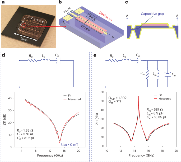
a, Photograph of the chip with multiple devices and a marked device, from which the measurement results are plotted in this figure. b, A 3D schematic of the resonantly coupled hairclip resonator. This schematic is exactly the same as the previously discussed HYG resonator. The difference is only visible in the cross-sectional schematic, as shown in c. c, Cross-sectional representation of the resonantly coupled device shows a capacitor formed between the ground plane and the top-side metal layer. This capacitor results in a self-resonance of the excitation transducer, which is visible in the measured impedance response in the absence of an external bias field. d, Equivalent circuit and measured impedance response of the device in the absence of any external bias. The measured impedance is fitted to a series LCR circuit, and the fitting parameters are fixed for the subsequent fitting of the measured MSW resonance. e, Equivalent circuit and measured response fitted to the circuit model. The device response was measured with an external bias of 685 mT. The circuit parameters C0, L0 and R0 correspond to the electrical capacitance, inductance and resistance of the metal trace, respectively. Meanwhile, Cm, Lm and Rm represent the equivalent capacitance, inductance and resistance of the magnetostatic branch.
Source data
Figure 5 summarizes the working principle of RHYG resonators with measurement results from one device (C1) on the chip. The overall profile of this device is exactly the same as the HYG resonator described earlier. However, the cross-sectional profile (Fig. 5c) is different in the sense that the top transducer and bottom ground plane are separated by a thin GGG layer left during the backside etching step. The equivalent circuit and measured impedance response of this device in the absence of an external biasing field are shown in Fig. 5d. The measured response fitted to the equivalent circuit and the corresponding fitting parameters R0, L0 and C0 are obtained. These parameters are fixed during the subsequent fitting of the measured data in the presence of an external bias. The equivalent circuit of the device in the presence of an external biasing field is shown in Fig. 5e. A parallel LCR branch is added to the previous circuit to represent the MSW. This circuit is fitted to the measured data with an external bias of 734 mT, and the corresponding fitting parameters are reported. Since the increased separation between fs and fp does not translate to increased magnetic-energy storage in the YIG, we do not define an effective coupling coefficient for these devices. The RHYG resonator demonstrates a separation of 1.1 GHz between fs and fp at 14.6 GHz, compared with a 0.5 GHz separation for the HYG resonator at the same frequency.
Comparison with state-of-the-art acoustic resonators
In this section, we compare the performance metrics of HYG resonators with recently reported acoustic resonators. As stated earlier, acoustic resonator technology is continuously being scaled for higher frequencies, including millimetre waves. The goal has been to maximize the ({k}_{t}^{2}Q) figure of merit (FOM) of these resonators through various techniques, such as new materials or new resonator design. We compile the performance metrics, that is, ({k}_{t}^{2}), Q and ({k}_{t}^{2}Q) FOM, from 12 recent acoustic resonators in 6–20 GHz frequency range5,11,32,33,34,35,36,37,38,39,40. We show a comparison between the reported acoustic resonators with HYG resonators in Fig. 6. We would like to point out that different papers report Q derived from different methodologies. These may include the 3 dB bandwidth method (Q3dB), circuit fitting (Q3dB) and Bode Q (ref. 41). Moreover, the reported Q might be at different frequency points, such as at series resonance (Qs), parallel resonance (Qp) or a frequency at which Q is the maximum (Qmax). The majority of the data points used in Fig. 6 are Qs obtained from the 3 dB bandwidth method. Although both Qs and Qp are relevant for different practical applications, we focus on comparing Qs of acoustic resonators with Qp of MSW resonators. This is because these parameters correspond to the frequencies at which a significant portion of the input electrical energy is converted into acoustic resonance or MSW resonance, respectively. For a detailed comparison of Qs and Qp values for both resonator types, please refer to the chart shown in Supplementary Section 3.1.
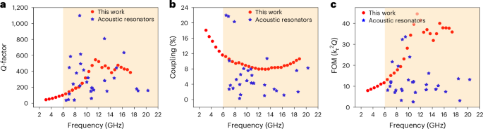
a–c, Q-factor (a), coupling coefficient (b) and ({k}_{t}^{2})Q FOM (c) of recently reported acoustic resonators compared with hairclip YIG resonators presented in this Article. Comparison is in the >5 GHz range as marked by shaded region.
Source data
As evident from Fig. 6, the hairclip technology competes well with acoustic resonators in the <10 GHz range and outperforms the acoustic technology in >10 GHz. The goal of HYG resonators was to increase the coupling. Although we lose a significant fraction of Q when trying to achieve a higher coupling, the Q remains comparable to most acoustic resonators. As systems move towards higher frequencies for applications like 5G, radar and satellite communications, the need for resonators that maintain high performance at these frequencies becomes critical. This positions HYG resonators as a key technology in next-generation filter designs, in which maintaining low loss and high selectivity at these higher frequencies becomes increasingly challenging for acoustic resonators.
Conclusion
MSW resonators are a potential platform for high-performance communication filters, especially for higher (more than 6 GHz) frequency ranges, and state-of-the-art thin-film YoG resonator technology offers exceptional f × Q product19. However, there are two main challenges currently limiting practical applications of MSW filters: the required bulky and power-hungry biasing magnets, and low coupling. A compact biasing permanent magnet with temperature compensation has been recently reported for 20 GHz fixed-frequency operation with out-of-plane bias42. A zero-quiescent-power biasing assembly has also been demonstrated for tunable filter frequency in the 3.4–11 GHz range17.
We have created MSW resonators with improved resonator coupling. This was achieved by developing a microfabrication technology for patterning GGG substrates. Our devices, which have a hairclip inductive loop around a YIG mesa resonator, exhibit a coupling of more than 8% in a wide frequency range (3–20 GHz) and are, thus, suitable for a tunable filtering approach. These hairclip resonators have the potential to be used in communication filters. They address challenges related to coupling and could lead to more efficient and tunable filters in wireless communication systems. Recent research has demonstrated tunable filters using the YoG material platform17,20,22, and our resonator technology could potentially be used to build filters based on such filter topologies. Furthermore, the approach could also be of use in the design of other coupled systems for quantum information science. Coupling magnons with microwave photons43,44 and phonons45,46,47,48,49 is an active research area, and we have demonstrated an example of avoided anti-crossing between magnons and microwave photons at room temperature (Supplementary Section 3.5). With appropriate superconducting metals, our fabrication technology could be used to create compact coupled systems to work at low temperatures for quantum applications.
Methods
Microfabrication
The fabrication of the HYG resonator starts with a 3-inch YoG wafer with a 3-μm-thick YIG layer on a 500-μm-thick GGG substrate. We dice the wafer into 1.5 cm × 1.5 cm pieces. Although we choose to process smaller chips to reduce the cost of the experiment, the process is scalable to the wafer size. The rest of the processing is performed on 1.5 cm × 1.5 cm pieces. We start by defining the rectangular YIG patterns on the chip using ion milling and subsequent soaking of the chip in H3PO4 at 70 °C to remove the redeposited material during the ion-milling process. After the YIG patterning, we deposit seed metal layers of titanium (Ti) and gold (Au) (Ti/Au, 10/300 nm) using the glancing angle deposition (GLAD) method. The seed layer is patterned by lithography and the wet patterning of Au and Ti layers. This patterned seed layer is used to deposit 1 μm Au using electroplating. The patterned electroplated Au serves as the hard mask during GGG patterning in the next step. A shallow (12 μm) etching of GGG is performed by utilizing phosphoric acid (H3PO4) at 160 °C. The etch rate of GGG is ~ 0.4 μm min–1 in H3PO4 at 160 °C (Supplementary Fig. 4). The hard-mask layers (Au/Ti) are stripped from the chip through wet chemical etching. The cross-sectional schematic of the chip after this step is shown in Fig. 4c, and the corresponding optical image is shown in Fig. 4h. The next step is patterned electroplating to define the top metallic transducers. For this step, a seed layer of a Ti/Au/Ti/Au (10/150/25/150 nm) stack is deposited using the GLAD method. A photoresist pattern was developed on the chip, and patterned electroplating of 6 μm gold was carried out. A Ti (100 nm) layer was deposited after the electroplating step, and lift-off was carried out. The partial seed layers (Au/Ti/Au, 150/25/150 nm) were removed using wet chemical etching with the Ti mask layer. Finally, the Ti seed and Ti mask were stripped using a buffered oxide etch solution, leaving the patterned top transducers. The details of the process are available elsewhere27. The chip was then thinned to a thickness of 100 μm. Figure 4d shows the schematic after completing this step. The top side of the chip was deposited using SiO2 (0.7 μm using plasma-enhanced chemical vapour deposition) and an electroplated Au layer using the GLAD-deposited metals (Ti/Au) as the seed layer. This SiO2/Ti/Au layer serves as a protection for the subsequent processing steps. Next, a patterned seed layer of Ti/Au (10/300 nm) is deposited on the backside of the chip, and electroplating is carried out to get a 1-μm-thick Au mask. The chip is then processed in H3PO4 at 160 °C for ~4.5 h with intermittent metrology steps to track the progress of etching. At this point, we have completely removed the GGG and Ti adhesion layer under the shallow-etched regions (defined in Fig. 4c) and leaving 3–8 μm GGG under the YIG layer. Subsequently, the top protection layers (Au/Ti/SiO2) are stripped using the respective etchants. Figure 4f,i illustrates the cross-sectional profile and optical image of the chip after this step. We emphasize the choice of seed layers (Ti/Au/Ti/Au) for the top metal traces in Fig. 4d, as the bottom Au/Ti layers are lost during this stripping process. We deposit blanket Ti/Au layers using GLAD and use electroplating to achieve a 2-μm-thick gold layer, which serves as the ground plane in our measurement.
Responses