High-sensitivity nanoscale quantum sensors based on a diamond micro-resonator

Introduction
Quantum systems comprising solid-state electronic spins have the potential for use as sensitive quantum sensors for various physical quantities1. Among the candidates for quantum sensing, a nitrogen-vacancy (NV) center in a single-crystal diamond is considered a leading candidate for a room-temperature quantum sensor that can precisely probe physical quantities, including temperature, strain, and electric fields2. In particular, it has shown considerable promise as a magnetometer for a wide range of applications, owing to its long spin coherence time. For instance, magnetic sensing based on a single NV center facilitates the nanoscale detection of chemical and biomedical information3,4,5 and fundamental spin dynamics6,7,8. Moreover, magnetic field sensitivities of the order of picoteslas have been achieved by employing an ensemble of NV centers (with a typical density of (sim)1017 cm−3)9; these are beneficial for medical applications requiring the detection of weak magnetic fields from the brain and heart10.
To build compact, practical, and scalable sensors, diamond sensors are miniaturized by combining optical fibers and complementary metal-oxide-semiconductor architectures11,12,13. However, these demonstrations tend to rely on bulk optics, which are typically limited to scales of several centimeters. To this end, one of the promising solutions is to integrate the sensor devices on-chip, which is inspired by recent advancements of photonic integration in quantum photonic information processing14,15,16 and classical laser systems17,18.
Another outstanding challenge in quantum sensing is the realization of solid-state magnetometers exhibiting both a high spatial resolution and magnetic field sensitivity. When such a spatial resolution is achieved using point defects in diamonds (as shown in Fig. 1a), the poor photoluminescence (PL) of these defects limits the magnetic sensitivity to several µT/(sqrt{{mbox{Hz}}}) even under coherent spin control. Furthermore, the extraction of photons from NV centers inside a probe tip or a nanodiamond is inefficient due to light scattering, which further degrades the field sensitivity19,20. This poor sensitivity is disadvantageous in terms of the data acquisition times. For instance, scanning magnetic images using the probe approach takes several hours with data points of several hundred for a better signal-to-noise ratio15. Enhancing field sensitivity enables real-time detection and monitoring of weaker magnetic fields by significantly reducing data acquisition times, which currently take several tens of minutes. By contrast, the use of an ensemble of NV centers is advantageous for achieving high sensitivity by increasing the total fluorescence of NV centers, as depicted in Fig. 1b. These NV centers are uniformly created in millimeter-scale bulk diamonds through electron beam irradiation, thereby sacrificing spatial resolution. The bulk structure also suffers from low photon collection efficiency due to the total internal reflection of the diamond substrate21. The demonstrated sensitivity of diamond magnetometers is still three orders of magnitude lower than that of other quantum sensors, such as superconducting quantum interference devices (SQUIDs) and optically pumped magnetometers (OPMs)22.

a Standard nanoscale diamond probe containing a single nitrogen-vacancy (NV) center. b Standard bulk diamond substrate that contains an ensemble of NV centers. c Proposed sensor structure based on diamond ring resonators possessing high-density NV centers.
In this study, we report high-sensitivity microscale and nanoscale quantum sensing by using on-chip diamond micro-ring resonators, as shown in Fig. 1c. A ring resonator enables the efficient use of photons emitted from the ensemble of NV centers by confining them in a nanoscale region. Recent breakthroughs in the etching technologies for single-crystal diamonds have led to a wide variety of nanophotonic structures23, such as photonic crystals24,25,26,27, photonic waveguides28,29, and ring and disk resonators30,31,32. By introducing diamond nanofabrication technology into quantum-sensing systems, we demonstrate on-chip micro-ring resonators containing a large number of NV centers. Hybrid integration based on pick-and-place operations facilitates the realization of a high-Q nanocavity on a cutting-edge photonic chip platform. We demonstrate coherent spin manipulation on a chip with an electron-spin resonance contrast approaching the theoretically expected value of 30%33. We also demonstrate that this tiny resonator possesses a magnetic sensitivity of 1.0 μT/(sqrt{{mbox{Hz}}}). Furthermore, we confirm that the nanocavity-based approach can achieve an improved sensitivity of up to 1.3 nT/(sqrt{{mbox{Hz}}}) by leveraging waveguide structures based on cutting-edge, high-quality integrated photonics to efficiently extract photons. Our on-chip sensing device provides a pathway for chip-scale packaged sensing to detect various nanoscale physical quantities for fundamental science, chemistry, and medical applications.
Results
Device fabrication
Figure 2 shows the basic flow for fabricating diamond micro-ring resonators for quantum-sensing applications. First, we prepared air-suspended silicon nitride (SiN) hard masks for the fabrication of the diamond ring resonators (see Methods for details). Transfer printing was employed to pick up and print them on the diamond using a transparent adhesive film made of polydimethylsiloxane (PDMS) ((Fig. 2a, b)34,35. This approach facilitated the fabrication process targeting a small single-crystal bulk diamond substrate that contains an ensemble of NV centers36. We employed a diamond substrate with an NV density of 5.3 (times ,)1016 cm−3 and a chip size of 3 × 3 × 0.5 mm3 (DNV-B1, Element Six). Next, the ring resonators were patterned on the diamond NV substrate by performing oxygen-based vertical dry etching and subsequent angled etching (Fig. 2c)24. Figure 2d displays a scanning electron microscopy (SEM) image of the fabricated structures. The ring structures connected to the diamond substrate were formed by carefully adjusting the time of the angled etching. The angled-etching process was also optimized to reduce burrs on the ring surface.
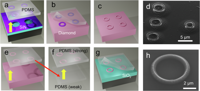
a–c Procedure for fabricating diamond ring structures. d Scanning electron microscopy (SEM) image of the fabricated ring structures. e–g Procedure for integrating diamond ring structures on a photonic chip. h SEM image of the diamond NV ring resonator integrated on SiO2. PDMS polydimethylsiloxane.
Next, we employed “pick-flip-and-place transfer printing” to integrate the ring resonators on a photonic chip36. This technique ensures deterministic hybrid integration by achieving a flat interface between the diamond nanostructure and photonic chip. The ring structure was lifted by the rapid motion of the PDMS film with weak adhesion (PF-40 × 40-0065-X0, Gel-Pack) (Fig. 2e). This film was flipped, and the ring structure was transferred to the PDMS with stronger adhesion (PF-40 × 40-0065-X8, Gel-Pack) (Fig. 2f). Finally, the ring structure was placed on the low-refractive index material of SiO2 by slowly peeling off the adhesive film as shown in Fig. 2g. Figure 2h displays an SEM image of the ring resonator that was flipped and integrated onto the SiO2 substrate. Considering the size of the ring structure, the number of NV centers in the resonator is estimated to be (2times {10}^{4}.,)Note that our approach, based on pick-flip-and-place transfer printing, is a powerful method to form ring resonators of single-crystal diamonds aside from creating a membrane of single-crystal diamonds on other substrates37,38. In addition, our approach is currently the only method for fabricating diamond ring resonators with an ensemble of NV centers on different photonic platforms, due to the complexity of the ensemble NV center creation process.
Device characterization
We characterized the fabricated device by performing the µ-PL measurements. Details of the optical setup are provided in the Methods section and Supplementary Note 1. Figure 3a shows a typical PL spectrum recorded for the fabricated ring resonator having a radius of 1.3 µm and width of 440 nm. As the ring structure is based on a triangular waveguide, we can observe both the transverse electric (TE) and transverse magnetic (TM) modes in Fig. 3a. By fitting the PL data with the Lorentzian function (Fig. 3b), we determined the Q-factors of the TE and TM modes to be 1000 (2200) and 1300 (2300) for the ring radius and width of 1.3 (2.3) µm and 650 (800) nm, respectively. For comparison, we evaluated the Q-factors of the TE and TM modes for the ring resonator based on a finite-difference time-domain (FDTD) simulation. The simulated Q-factor Qsimu of TE and TM modes were 42,000 (1.8(times {10}^{6})) and 26,000 (1.5(times {10}^{6})) for the ring radius of 1.3 (2.3) µm at the resonant wavelength of ~700 nm. The discrepancy between the experimental values and the simulated calculations is likely due to the reduction in the width during angled etching (~200 nm narrower) and the surface roughness, not light absorption by an ensemble of NV centers. To confirm this, we also evaluated the contribution of absorption to the Q-factor as Qabs(,=frac{2pi n}{alpha {lambda }_{c},}), where ({lambda }_{c}) is the resonant wavelength of the cavity, n is the refractive index of diamond, and ({alpha }_{{NV}}) is the absorption constant of the ensemble of the NV centers. By using the reported absorption constant of ({alpha }_{{NV}}) = 0.45 cm−1 for the NV density of 2.3 (times ,)1016 cm−3 21, we deduced Qabs to be 2.3 (times ,)105 for the density of 5.3 (times ,)1016 cm−3 in this study. These results indicated that the bottleneck in the Q-factor is not the absorption of NV centers. We emphasize that the observed Q-factor was the highest in diamond nanocavities containing high-density NV centers. The demonstrated high-Q microcavity may be used to develop a nano-laser with a gain material of ensemble NV centers39, which might enable us to achieve femtotesla-scale sensitivity compatible with those of SQUIDs and OPMs, because spin-dependent lasing provides a large number of photons with a high measurement contrast40.
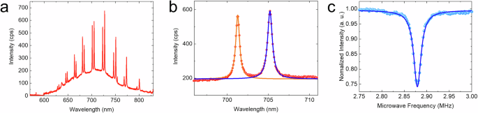
a Photoluminescence (PL) spectrum measured for the fabricated ring resonator with a radius of 1.3 µm. b PL spectrum of the cavity mode fitted by applying the Lorentzian function. The solid blue (orange) line shows data fit with the Lorentzian function for the waveguide TE (TM) mode. The Q-factors of the TE and TM modes are evaluated to be 1000 (2200) and 1300 (2300) for a ring radius of 1.3 (2.3) µm, respectively. c Optically detected magnetic resonance spectrum for the investigated ring resonator. The solid blue line shows data fit with the Lorentzian function, leading to an electron-spin resonance contrast of 25%.
We performed further detailed characterization of the fabricated devices. For this purpose, we implemented a microwave antenna of 120 µm near the ring resonators on a photonic chip (see Supplementary Fig. S2). Figure 3c shows the optically detected magnetic resonance (ODMR) spectrum for the investigated ring resonator. Owing to the efficient microwave excitation, we observed a clear ODMR dip with a contrast of 25%, which is close to the theoretically expected value of 30% when the spin states of(,{m}_{s}=pm 1) are degenerated. For comparison, the contrast of bulk diamond is typically ~1% because of inefficient and nonuniform microwave excitation36 (see Supplementary Note 2). Microwave fields typically cover areas on the order of several millimeters, which is comparable to the dimensions of bulk diamond substrates41. In contrast, nanostructures facilitate uniform microwave excitation due to their much smaller size relative to the microwave field. Consequently, we can confirm that the use of nanostructures is advantageous for achieving high contrast in ODMR.
Characterization of spin coherence
Next, we investigated the coherence times, T2* and T2, of the NV centers in the fabricated device. Before these investigations, we evaluated the pulse duration of the microwave π-pulse for the NV centers. The spin degeneracy in the investigated NV centers were lifted, and magnetic field was applied using a permanent magnet, as shown in the ODMR spectrum in Fig. 4a. Figure 4b shows the pulse sequence of the electron-spin Rabi oscillation at a microwave frequency of 2.77 GHz. The π-pulse duration was deduced to be 230 ns for our current setup. We applied a pulsed laser, π/2-pulse, and π-pulse as the pulse sequence depicted in the inset in Fig. 4c, d to evaluate the coherence times (see the Methods section). Figure 4c, d shows the decay curves of the investigated NV centers obtained via Ramsey interferometry and Hahn echo, respectively. The insets show the pulse sequences used for the measurements. The data were fitted using the cos ((2pi tau /{T}_{2pi })exp (-tau /{T}_{2}^{* })) function with a fitting parameter (({T}_{2pi })) to deduce the coherence time T2* to be 700 ns The data in Fig. 4d were fitted by using an exponential decay curve, resulting in a coherence time T2 of 6.0 µs The obtained coherence time was better than those of the nanodiamond42 and diamond nano-probes43. Although this comparison is not fair in terms of the depth of NV centers, the demonstrated longer coherence time offers an advantage for the new sensing regime, as discussed later. The decrease in the coherence time before etching the diamond (T2* = 1 µs, T2 = 200 µs) primarily stems from the surface roughness due to dry etching; such rough surfaces host defects that generate electric and magnetic field noise. We attribute the noise in Fig. 4b–d to electrical pulse jitters in acousto-optic modulators and controlling systems. This surface noise for the coherence time may be improved via oxygen surface termination44. The roughness of the sidewall of the ring resonator could also be ameliorated through oxygen-based optical near-field etching42. We also confirmed that the proposed nanofabrication processes had little effect on charge states of NV centers (see Supplementary Note 3).
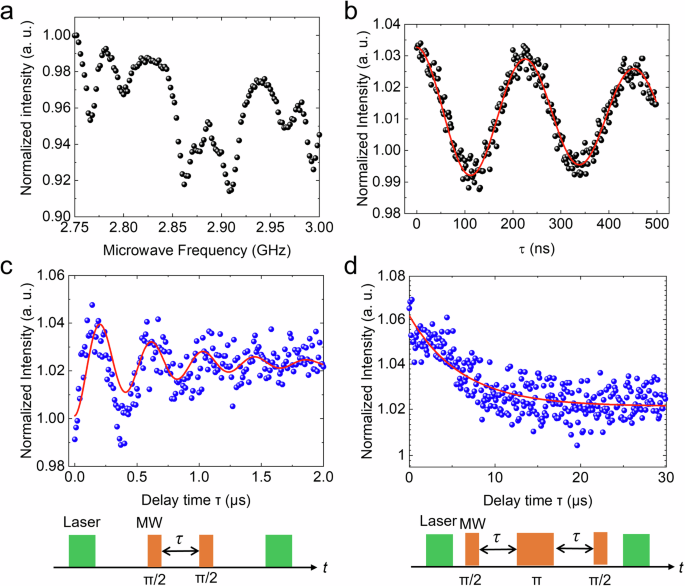
a ODMR spectrum for the investigated ring resonator under a static magnetic field. b Rabi oscillations of transitions for a microwave frequency of 2.77 GHz. The red solid line denotes an exponentially damped sinusoidal fit to the data. c Decay curves of Ramsey interferometry for the investigated NV centers. The solid red line indicates data fit by applying the cos ((2pi tau /{T}_{2pi })exp (-tau /{T}_{2}^{* })) function with a fitting parameter, ({T}_{2pi }) resulting in a coherence time of T2* = 700 ns The inset shows the pulse sequence of the green laser and microwave (MW) used for Ramsey interferometry. d Decay curves of Hahn echo measurements on the investigated NV centers. The solid red line indicates the exponential decay fit, yielding a coherence time of T2 = 6.0 µs. The inset shows the pulse sequence used for the Hahn echo.
Evaluation of field sensitivity
Finally, we evaluated the sensitivity of the device to a magnetic field. Figure 5a shows the basic principle of lock-in detection for evaluating the sensitivity. The microwave frequency was fixed at 2.8724 MHz. We then applied a magnetic field of 1 kHz using a circular coil (10 mm radius with six turns) located underneath the device and attached it to the glass-based sample holder (see Supplementary Fig. S5). The oscillation of the magnetic field induced a fluctuation of the dip in the ODMR spectrum, which was detected using a lock-in amplifier with an oscilloscope12.
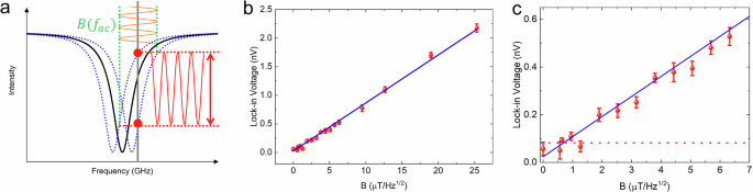
a Basic principle of lock-in detection used to evaluate magnetic field sensitivity. b Detected lock-in voltage as a function of the intensity of the applied magnetic field. The solid blue line shows data fit with a linear function. c Magnified view of the area with a weak magnetic field depicted in b. The purple dotted line shows the estimated noise floor. Error bars are defined by the standard deviation of measured data points.
Figure 5b shows the detected lock-in voltage as a function of the intensity of the applied magnetic field in µT/(sqrt{{mbox{Hz}}}) The magnetic fields applied to the diamond cavity were determined using the Biot–Savart law. To estimate the minimum detectable magnetic field, we performed a linear fit on the obtained data, represented by the solid blue curve in Fig. 5b. Figure 5c shows a magnified view of the area with a weak magnetic field displayed in Fig. 5b. The fittings are consistent with the data obtained for B < 0.2 μT/(sqrt{{mbox{Hz}}}). We assumed that the noise floor in this study was ~0.1 nV (dotted purple line in Fig. 5c). The fitted results and noise floor level were utilized to estimate the minimum detectable magnetic field for this device to be 1.0 μT/(sqrt{{mbox{Hz}}}). For comparison, the typical DC sensitivities based on a single NV center range from 2–10 μT/(sqrt{{mbox{Hz}}})6,43,45 We note that other studies employ complicated pulse techniques to improve magnetic field sensitivity46. However, such techniques are challenging to implement in compact and practical device architectures. In contrast, our experimentally demonstrated sensitivity of 1.0 µT/(sqrt{{mbox{Hz}}}), achieved without the use of any pulse techniques, represents an important milestone toward the development of practical quantum sensor devices. Therefore, our cavity-based NV sensor offers sufficiently high spatial resolution and sensitivity.
Waveguide-coupled structure for improving sensitivity
We demonstrate that further improvement in the field sensitivity of the developed system is possible by introducing a state-of-the-art waveguide for diamond quantum sensing. Figure 6a shows a schematic of the investigated structure, where the diamond ring resonator is heterogeneously integrated beside a SiN low-loss waveguide47, which is compatible with complementary metal-oxide semiconductor technology48 and thus may enable the construction of compact and functionalized quantum-sensing devices. We simulated the emitter-to-waveguide coupling based on the FDTD method. We assumed that the zero-phonon line (ZPL) of the NV emission is resonant with the cavity TE mode (637 nm). We set a ring radius (width) of 2.3 µm (700 nm) and the SiN waveguide width (height) at 400 (200) nm. The ring was attached onto the sidewall of the waveguide (Fig. 6a), which required no positional alignment and facilitated the hybrid integration process of transfer printing. Based on the simulated loaded (unloaded) Q-factor of the ring resonator of 5.7(times {10}^{4}) (1.1(times {10}^{6})) at the ZPL wavelength, the cavity-to-waveguide coupling efficiency was calculated to be 95%. The investigated ring structure also has a relatively small mode volume of 0.32 µm3, which provides a high emitter-to-cavity coupling efficiency of 94% even under the low Debye Waaler factor of 5%. The emission of the NV center is coupled to the SiN waveguide, as shown in Fig. 6b, providing a coupling efficiency ({eta }_{{{rm{NV}}}}) of 89% (see Supplementary Note 4). This structure improves the photon collection efficiency by up to 18-times compared with a ring resonator without a waveguide (see the Methods section). It is notable that achieving ultra-high-Q-factors in diamond cavities is challenging, especially using tiny nanostructures. We believe that the so-called “smart-cut” approach of high-quality thin-film diamond membranes would greatly improve the Q-factors of cavities in diamond37,38.
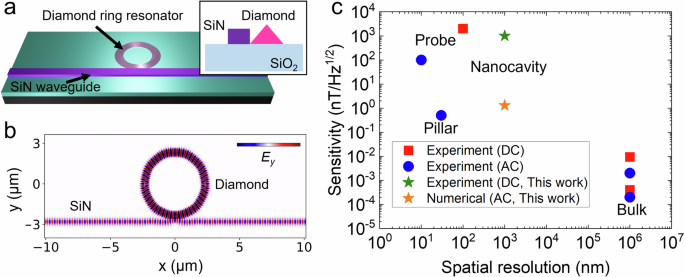
a Schematic of the investigated diamond ring resonator optically coupled to a SiN low-loss waveguide. Inset: cross-section of the investigated structure. b Electric field distributions (Ey component) of the cavity resonant mode at 637 nm. c Comparison of the sensitivity of the cavity-based approach with those of other diamond quantum sensing systems. The experimental sensitivity data indicated by the red and blue points are obtained from the literature43,46,51,52,53,54. We assume that the spatial resolution of sensing with a diamond substrate is restricted by the chip size (~1 mm).
Next, the magnetic sensitivity of the proposed device structure was evaluated. The AC magnetic sensitivity of NV centers is described in the following expression19:
where ({{hslash }}) represents the Planck constant, (gapprox 2) is the electronic g-factor, ({mu }_{{B}}) is the Bohr magneton, C denotes the ODMR contrast, and ({I}_{{count}}) is the photon count rate of NV centers. For a saturation excitation power of 10 mW, ({I}_{{count}}) was estimated to be 21 mega counts/s (Mcps) considering the aforementioned photon extraction efficiency ({eta }_{{{rm{NV}}}}) and the fact that the photon count rate without the cavity is 1.2 Mcps. We also employed ({T}_{2}) = 6.0 µs, which was obtained in this study. Utilizing these values, the sensitivity of the device was calculated to be 1.3 nT/(sqrt{{{rm{Hz}}}}). This sensitivity is superior to that of AC sensing with a single NV center (~100 nT/(sqrt{{{rm{Hz}}}}).)46,49,50. Figure 6c presents the reported sensitivities as functions of the spatial resolution43,46,51,52,53,54. The best field sensitivity reaches 0.5 nT/(sqrt{{{rm{Hz}}}}) for a single NV center, and 210 fT/(sqrt{{{rm{Hz}}}}) for ensemble NV centers53. Meanwhile, our proposed approach, based on cavities with typical widths and heights of several hundred nanometers, can achieve both high sensitivity and nano-to-microscale spatial resolution by balancing the tradeoff between these two parameters on a single integrated photonic chip. We note that the dead time of avalanche photodiodes is typically 20 Mcps. We can overcome this limitation by using silicon photomultipliers or superconducting nanowire single-photon detectors as alternatives. It is also notable that resonant excitation could enhance field sensitivity by increasing NV photon output55,56,57, though this technique requires cryogenic temperatures and precise laser filtering.
Discussion
We have demonstrated nanoscale and sensitive quantum sensors based on diamond micro-ring resonators. A high-Q diamond ring resonator containing numerous NV centers was successfully fabricated by combining diamond nanofabrication with pick-flip-and-place transfer printing. This chip-based approach is advantageous for miniaturizing sensor devices by exploiting the power of cutting-edge integrated photonic technology11,12,13. Through the coherent spin manipulation of NV centers on a chip, we achieved a magnetic sensitivity of 1.0 μT/(sqrt{{mbox{Hz}}}) for the developed nanoscale device with an electron-spin resonance contrast of 25%. We also numerically demonstrated that our microcavity-based platform further improves the field sensitivity (1.3 nT/(sqrt{{{rm{Hz}}}})) via combination with SiN photonics. The enhancement of field sensitivities significantly reduces data acquisition times and enables real-time detection and monitoring of weak magnetic fields. The proposed diamond sensor with sub-nT sensitivity readily facilitates imaging the information based on magnetic fields that require micrometer precision, such as living cells of bacteria58, neuron59, and geological samples60. By employing tiny photonic cavities such as photonic crystals, we can advance the detection of signals in smaller regions. If NV centers are shallowly implemented in diamond resonators, the proposed approach can also provide sub-nanometer distances between NV spins and samples with better spin coherence times61 when investigating quantum magnetic phenomena in 2D materials62,63,64. This system would also be useful to perform nano magnetic resonance imaging65 and nuclear magnetic resonance measurements50,66. This study, based on a photonic chip, paves the way for nano-to-microscale sensitive quantum sensing, which is required in a wide range of fields, including condensed matter physics, chemistry, neuroscience, and medicine.
Methods
Fabrication of SiN hard mask
Air-suspended SiN structures were prepared as hard masks for diamond etching. We used a 200-nm-thick SiN layer deposited on a SiO2/Si substrate with a SiO2 thickness of 1 µm. The cavity structures were patterned with a positive polymer resist (ZEP520A) as a mask using electron beam lithography and subsequent CF4-based dry etching processes. O2 plasma ashing was then performed to remove the residual polymer resistance. The structure was air-suspended through chemical wet etching with buffered hydrofluoric acid, followed by the drying process with a critical point dryer.
Fabrication of diamond ring resonators
The diamond ring resonators were fabricated using the SiN hard masks. After printing the masks to diamond, we transferred the patterns to the diamond by using inductively coupled plasma reactive ion etching with O2/Ar plasma. The sample was then placed inside a conical Faraday cage and undercut with angled plasma under the same condition of dry etching with vertical etching. The residual hard masks were removed by wet etching with buffered hydrofluoric acid.
Optical setup
The measurements were performed at room temperature. The device was placed on a stage equipped with a three-axis piezo actuator (Physik Instrumente, P-517.3CL) in order to control the sample positions precisely. The NV centers in a diamond ring resonator were optically pumped by using a stable continuous-wave laser oscillating at 532 nm (Laser Quantum, Gem 532). A ×50 objective lens (Olympus Corp., LCPLN50XIR,) was employed for the observation and excitation of diamond nanostructures. We used a dichroic mirror to guide the green laser to the sample and filter it out for signal detection. The signal was collected by using the same lens and sent to the spectrometer equipped with a silicon charge-coupled device (CCD, Princeton Instruments, PIXIS256E) camera through the notch filter (533 nm). The excitation power was set to 6.2 mW during the measurement of the PL spectrum presented in Fig. 3a.
For the ODMR measurement, we switched the CCD camera to a sensitive single-photon avalanche photodiode (APD, Micro Photon Devices, PDM PF5CTB). Microwaves were generated from a source (Anritsu, MG3740A) with an amplifier (Mini-circuit, ZHL-16W-43+) to control the spin states of NV centers. A microwave was applied to the sample via a microwave antenna of 120 µm on a photonic chip (see Supplementary Fig. S2). ODMR spectra were obtained by accumulating signals while sweeping the microwave frequency.
The spin coherence times of NV centers were evaluated by using an acousto-optic modulator (AOM, ISOMET, M1201E-SF40-1.7 V) in combination with a pulse generator (Tektronix, DTG5274) to generate pulsed green laser. π-pulse was generated to manipulate the spin state by using the same pulse generator with a fast microwave switch (Mini-circuit, ZASWA-2-50DR+). For the evaluation of the sensitivity of the device to a magnetic field, the magnetic field was generated by applying the AC voltage to the coil attached to the sample holder. The microwave frequency was fixed at 2.8724 MHz. We measured the PL using the aforementioned APD while sweeping the power of the AC voltage and analyzed the data with a lock-in amplifier (Stanford Research Systems, SR830). For the lock-in detection, we set the frequency of an AC magnetic field to 1 kHz. The intensity of the magnetic fields in µT/(sqrt{{mbox{Hz}}}) applied to the diamond cavity was determined using the Biot–Savart law and the frequency of the AC voltage.
Numerical simulation
The resonant modes of the ring resonators are investigated by commercial software Tidy 3D based on FDTD simulation. The details of calculating ({eta }_{{{rm{NV}}}}) are shown in Supplementary Note 4. We evaluated the extraction efficiency of the ring resonator without the SiN waveguide by assuming that the NV center is a dipole source oscillating along the y axis in Fig. 6b at the wavelength of 637 nm. Since the signal is collected by the objective lens with a high numerical aperture, the extraction efficiency is the ratio of photons scattered in +z axis. By monitoring the radiation power distribution, we deduced the extraction efficiency of the NV emission to be 5%.

Responses