Intrinsically anisotropic 1D NbTe4 for self-powered polarization-sensitive photodetection
Introduction
Polarization-sensitive photodetection has the capability to capture a broader range of scene information, which has significant application potential in wide-range fields, such as imaging, monitoring, remote sensing1,2,3,4,5,6. To achieve polarization detection with high sensitivity and versatility, it is necessary to utilize an active layer with highly anisotropic behaviors in polarized photodetectors7,8,9,10. Early research primarily focused on macroscopic anisotropic materials that required complex geometric processing, which was not conducive to device integration and miniaturization7,11,12. Compared with the traditional photodetectors, polarized light detectors based on anisotropic low-dimensional materials can directly use the intrinsic anisotropy of materials to sense polarized light, which has a good application prospect for future optoelectronic applications13,14,15,16. Therefore, the exploration of low-dimensional materials with low-symmetric crystal structures that possess intrinsic anisotropic optical and electronic properties has aroused considerable interest. In recent years, the emerging of in-plane anisotropic two-dimensional (2D) materials, such as BP17, GeSe18, ReSe219, PbSe220 and TaFeTe421, have become promising candidates for polarization-sensitive photodetection owing to their intrinsically sensitive to linearly polarized light and compatibility with modern silicon processes. In addition, in the family of anisotropic low-dimensional materials, one-dimensional (1D) structures have inherent anisotropy and can be also used as photoactive materials22,23,24,25, showing great prospects in the field of polarized light detection. As such, it is also of great application value to explore one-dimensional anisotropic materials for polarized light detection.
1D crystal-structural materials, usually consisting of parallel atomic chains that extend indefinitely along the high-symmetric axis. Due to the distinct differences in atomic arrangement and bonding patterns in the in-chain direction and perpendicular to the chains, 1D crystal-structural materials exhibit natural phonon vibration, optical, and electrical anisotropy22,26,27. These inherent properties make them the promising functional components in polarization-sensitive optical, electronic and optoelectronic devices. NbTe4, a transition metal tetra-chalcogenides, has been demonstrated some unique physical properties that originate from its quasi-1D structure. For instance, NbTe4 is a superconductivity material under pressure conditions28. Subsequently, NbTe4 also has been observed that Te deficiency can significantly enhance the charge density wave (CDW) resistivity anomaly near 200 K and lead to a superconductor state emerges at 5.5 K29. In addition, the polarization sensitivity of phonon vibrations has also been revealed by Raman spectroscopy30. Most studies have focused on phase transitions, but there are few studies on its optical and photoelectric anisotropy, even though NbTe4 crystals are a quasi-1D material with natural anisotropy. Moreover, due to the chains being connected by weak van der Waals forces and the 1D characteristics of the chain structure, 1D crystal-structural materials can be stripped into nanostructures with anisotropic geometry. The inherent one-dimensional anisotropic crystal structure combined with the external geometry morphology will make their easier to obtain distinct optical, electronic, and photoelectric anisotropy. Therefore, NbTe4 is regarded as the promising functional components for high-performance polarized photodetection.
The 1D material NbTe4, distinguished by its needle-like morphology, has been successfully synthesized and utilized for polarized light detection. The relationship between Raman intensity and angle was investigated using angle-resolved polarized Raman spectroscopy (ARPRS), with the results aligning with those obtained through density functional theory (DFT) calculations. Furthermore, azimuth-dependent reflectance difference microscopy (ADRDM) reveals that 1D NbTe4 exhibits intrinsic in-plane optical anisotropy. Remarkably, 1D NbTe4 device exhibits the obvious polarization-sensitive photodetection characteristics with a dichroic ratio up to ~1.16 at 671 nm and ~1.25 at 1064 nm. Concurrently, such device exhibits a significant photothermoelectric effect, enabling a broad spectral photoresponse ranging from the visible to the near-infrared spectrum (532-1064 nm), with a rapid response time of 158 ms at 671 nm. Our findings show that 1D NbTe4 has natural in-plane optical anisotropy, making it highly promising for future optical anisotropic devices.
Results and discussion
NbTe₄ crystallizes in a one-dimensional anisotropic molecular chain structure (Fig. 1a, b), which belongs to the space group P4/mcc (124) with lattice parameters a = 6.449 Å, b = 6.449 Å, and c = 6.837 Å. Nb (red spheres) and Te (blue spheres) atoms are interconnected to form one-dimensional chains along the c-axis, with each Nb atom coordinated to eight slightly distorted square antiprism Te atoms. These one-dimensional (1D) chains are aligned parallel to the a-axis (and b-axis) direction and are interconnected via relatively weak van der Waals interactions. Consequently, the atomic configurations along the chains exhibit substantial differences compared to those in the perpendicular directions. Therefore, the structures of NbTe4 are intrinsically anisotropic, rendering them promising candidates for anisotropic device applications. Given that the chains are connected by weak van der Waals forces, NbTe4 single crystals can be mechanically exfoliated to investigate the physical properties of their 1D nanostructures. Furthermore, high-quality NbTe4 single crystals were synthesized using the chemical vapor transport (CVT) method (Fig. 1c), with the optical image of bulk single crystals and nanosheets provided in Fig. S1. Due to its one-dimensional chain structure, the crystal morphology of NbTe4 exhibits a needle-like form. The X-ray diffraction patterns of the powder samples match the standard NbTe4 spectrum, and the needle-like bulk samples show excellent orientation, indicating high-quality NbTe4 single crystals (Fig. 1d). Scanning electron microscopy (SEM) and the energy dispersive X-ray spectroscopy (EDS) shows the atomic ratio of Nb: Te is 1.04: 3.96 (Fig. 1e), which is consistent with the atomic ratio of NbTe4 as previously reported. To further understand its crystalline structure, transmission electron microscopy (TEM) was employed (Fig. 1f, g). High-resolution TEM (HRTEM) images reveal a relatively regular atomic arrangement, with an interplanar distance of d(002) = 3.31 Å. Furthermore, the atomic distribution of Nb and Te atoms aligns with the chain structure characteristic of NbTe4.
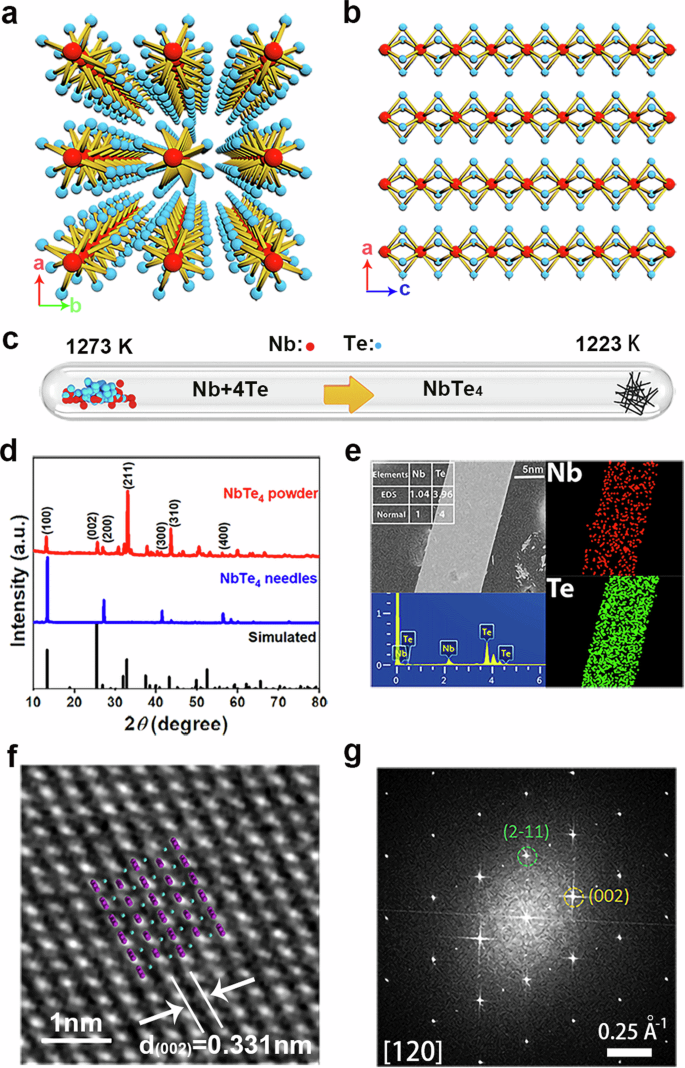
a Crystal structure of NbTe4 view along the c-axis and (b) b-axis. Red sphere: Nb atoms, blue sphere. c Schematic diagram of high-quality NbTe4 single crystals prepared by CVT method. The ratio of the precursor Nb and Te is 1:4. d X-ray diffraction (XRD) patterns of NbTe4 powder and bulk single crystals. e Scanning electron microscopy (SEM) image and energy dispersive X-ray spectroscopy (EDS) result, and corresponding element mappings for NbTe4 single crystal. f High-resolution transmission electron microscope (HRTEM) image of NbTe4 flake. g Corresponding fast Fourier transform pattern.
Raman spectroscopy is a powerful tool for investigating the vibrational and rotational dynamics of molecules within a crystal structure, thereby offering profound insights into the material’s physical properties, such as phase transitions and polarization characteristics. In this study, the Raman spectrum of bulk NbTe4 crystals was acquired at room temperature. As illustrated in Fig. 2a, seven distinct Raman peaks were observed range from 110 to 250 cm-1, specifically located at 126.3, 138.8, 146.1, 157.5, 165.8, 197.9, and 215.5 cm-1. The Raman mapping spectroscopy of NbTe4 is presented in Fig. S2, with the mapping at 138.8 cm-1 being the most distinct, aligning with the standard Raman spectrum. According to density functional theory (DFT) calculations (Fig. S3), these peaks correspond to the ({A}_{1text{g}}^{1}), ({A}_{1text{g}}^{2}), ({B}_{2g}), ({A}_{2g}), ({E}_{g}) and ({E}_{u}) modes, respectively. Notably, the ({E}_{u}) modes are Raman inactive in an undistorted P4/mcc structure. However, it is noteworthy that the experimental energy values closely align with the calculated phonon energies, and the ({E}_{u}) modes are observable in Fig. 2a, as previously reported. Additionally, the peak at 157.5 cm-1 lacks a corresponding calculated value. Similar anomalies have been reported for other charge density wave (CDW) materials, such as TaTe430 and GdTe331, which are attributed to minor lattice distortions induced by the breaking of inversion symmetry and CDW effects.

a The Raman spectroscopy of NbTe4 and corresponding Raman active modes. b Temperature-dependent Raman spectroscopy of NbTe4 from 77 to 623 K. c Temperature dependence of Raman shifts of ({A}_{1g}^{2}) and ({B}_{2text{g}}). d Angle-resolved polarized Raman spectroscopy. e False-color plot of the polarized Raman spectroscopy of spectroscopy, where the color reflects the intensity of the Raman peaks. f–h Polar plots of Raman peak intensity with polarization angle at 138.8, 197.9 and 215.5 cm−1, respectively.
Subsequently, temperature-dependent Raman spectra were analyzed to extract Raman temperature coefficients and investigate potential phase transitions within the temperature range of 77 to 623 K. As illustrated in Figs. 2b and S4, all Raman peaks of the NbTe4 nanobelts remained well-preserved up to 623 K, indicating exceptional high-temperature stability. Additionally, the environmental stability of NbTe4 was evaluated through its Raman spectroscopy (Fig. S5). As the temperature increases, the visible Raman peaks exhibit a redshift attributable to phonon anharmonic effects and the expansion of the crystal lattice. However, no significant or abrupt changes in the spectral peak positions were observed, indicating the absence of a CDW phase transition. Notably, NbTe4 undergoes a CDW transition within the temperature range of 150 K to 200 K32,33, a phenomenon that is not reflected in the Raman spectra, consistent with previous reports30. To characterize the temperature dependence of the Raman peak positions, the Grüneisen model34 (ω (T) = ω0 + χT) was employed, where ω0 represents the peak frequency at absolute zero (0 K) and χ denotes the first-order temperature coefficient. As illustrated in Figs. 2c and S6, all selected Raman peaks exhibit a nearly linear decrease as a function of temperature. The calculated values for the ({A}_{1g}^{1}) and ({B}_{2g}) modes were determined to be -0.01355 and -0.01246 cm-1 K-1, respectively, which are lower than those observed in other transition metal chalcogenides, such as MoTe235 and ReS236. Furthermore, angle-resolved polarized Raman spectroscopy (ARPRS) under parallel polarization with backscattering configurations can be utilized to identify crystalline orientation and phonon vibrations, thereby offering insights into in-plane anisotropic structures. Raman spectra of NbTe4 were collected at various angles by rotating the crystal using a rotational device. Figure 2d illustrates the Raman signals at different polarization angles, demonstrating that the intensity of the Raman peaks varies from minimum to maximum as the polarized light is rotated by 90°. To elucidate this change more distinctly, the corresponding contour color maps are presented in Fig. 2e, demonstrating that all peaks exhibit a periodicity of π. Concurrently, the intensity of Raman peaks under varying polarization angles was extracted as a function of the angle, and the fitted curves exhibit a periodicity of 180° with changes in the angle (Figs. 2f–h and S7). These findings corroborate the phonon vibration anisotropy of NbTe4 and offer deeper insights into the relationship between crystal structure and polarized Raman spectroscopy.
As a member of the transition metal tetra-chalcogenides characterized by an intrinsically anisotropic one-dimensional structure, the in-plane anisotropic optical properties of NbTe4 were investigated using azimuth-dependent reflectance difference microscopy (ADRDM) measurements. ADRDM is a nondestructive, in situ imaging technique that enables visualization of the reflection anisotropy of NbTe4 nanobelts. Figure 3a presents the initial optical microscopy image of NbTe4 nanobelts under polarized light, clearly delineating the sample from the substrate through the observed reflectance difference signals. In order to quantitatively describe the reflectance difference signals, the normalized reflectance difference (Δr) is defined as
where rx and ry are the reflectance rates along any two orthogonal directions of the sample surface (x and y), respectively, that is perpendicular to the direction of the incident light. The dimension-less value N(θ) is directly related to the reflectance intensity and periodically changes with the rotation angle (θ) of the linearly incident polarized light, which can be regarded as

a ADRDM optical image of NbTe4 on an isotropic SiO2/Si substrate. b Angle-dependence ADRDM results of NbTe4 in the area marked by the position 1 and (c) position 2 in (a). d ADRDM images of NbTe4 as a function of the rotation angle.
The initial polarization direction is defined as 0°, corresponding to the y-axis in the horizontal plane. By analyzing the extreme values of N(θ), the crystalline orientation of the low-symmetry crystals can be determined. Subsequently, two points on the sample were selected for ADRDM measurements, with the results for a NbTe4 nanobelt presented in Fig. 3b and c, respectively. The function N(θ) exhibits periodic variation with the angle of rotation of the incident polarized light from 0° to 360°, with maxima occurring at approximately 140°, indicating that the plane of linearly polarized light is parallel to the c-axis of NbTe4, and minima at approximately 50°. Notably, ADRDM enables direct in situ anisotropy comparisons of different materials by capturing the N(θ) signals across the entire field of view. Figure 3d illustrates the ADRDM images of the NbTe4 nanobelt under various polarized light angles ranging from 0° to 180°. For the isotropic SiO2/Si substrate, the reflectance difference signals exhibit negligible variation with the rotation angle of the polarized light, consistently maintaining a value of zero (green). In contrast, the reflectance difference signals of NbTe4 display significant changes, thereby confirming the pronounced optical anisotropy of NbTe4. The maximum intensity is observed at rotation angles between 135° and 145° (dark red), whereas the minimum intensity occurs between 45° and 55° (dark blue), corroborating the findings presented in Fig. 3b. Similar results also were obtained in other samples (Fig. S8). The measurement outcomes of ADRDM indicate that NbTe4 exhibits pronounced optical anisotropy. This characteristic serves as a foundation for further investigation into its potential applications in polarized light detection.
To investigate potential applications in the fields of electronics and optoelectronics, the optoelectronic performance of one-dimensional NbTe4 nanobelts was further characterized. The current-voltage (I–V) curves were measured under varying wavelengths and light power densities, as illustrated in Fig. 4a and S9. These measurements indicate that NbTe4 exhibits a broadband photoelectric response spanning from the visible to the near-infrared region. Notably, within a smaller voltage range, a significant photocurrent is observable even at zero bias voltage (Fig. 4a). To understand the photocurrent generation mechanism, the time-resolved photocurrent curves was measured at zero bias voltage. It is noteworthy that the photocurrent exhibits a positive response when the laser spot illuminates one end of the device, but transitions to a negative response when the light is positioned at the opposite end (Fig. 4b), indicating a significant photothermoelectric (PTE) effect. This phenomenon has been similarly observed in other low-dimensional materials, particularly tellurides, thereby offering an ideal platform for the development of self-powered photodetectors37,38,39.

a Typical I–V curves at different wavelength. b Time-resolved photocurrent curves under different wavelength at zero bias voltage. c Time-resolved dynamic photoresponse curves under different power density of 671 nm laser. d Iph–P and (e) R–P curves of the NbTe4 photodetector under different wavelength. f Rise and decay response time under 671 nm laser.
The time-resolved dynamic photoresponse curves under different wavelengths are presented in Figs. 4c and S10, demonstrating the stability and reproducibility of the 1D NbTe4 nanobelts photodetector. The photocurrent (Iph), defined as Iph = Ilight − Idark, was extracted under varying light power densities (P) and is depicted in Fig. 4d. By fitting the data to the exponential relationship Iph ∝ Pα, the factor α was determined to be 1.24, 1.28, and 1.41 for laser illuminations at 523, 671 and 1064 nm, respectively. The factor α, being greater than 1, can be attributed to the combined influence of the photoconductive effect and the photothermoelectric effect. Responsivity (Rλ), a critical parameter in photodetection, is defined as Rλ = Iph/PS, where Iph represents the photoinduced current, P denotes the power density, and S signifies the effective area of the device. The corresponding results are presented in Fig. 4e. Under identical conditions, the device demonstrates its optimal photoelectric response at a wavelength of 671 nm. Moreover, unlike the typical photoconductive effect, the responsivity (R) increases with rising incident power density, which can be attributed to the influence of the PTE effect. Additionally, the photoresponse speed was evaluated based on time-resolved dynamic photoresponse curves (Figs. 4f and S11). As shown in Fig. 4f, the rise and decay times are 171 ms and 158 ms, respectively.
1D NbTe4 exhibiting in-plane optical anisotropy and a superior optoelectronic response prompts further investigation into its performance in polarized light detection. A schematic representation of the NbTe4 polarized light photodetector is presented in Fig. 5a, where the angle of the linearly polarized light is adjusted by rotating the half-wave plate. As illustrated in Fig. 5b, under 671 nm laser irradiation, the photocurrent exhibits periodic variations as a function of the angle of linearly polarized light at zero bias voltage. The maximum polarized photoresponse current is observed at approximately 60°, while the minimum is observed at approximately 150°. To provide a more intuitive understanding of this phenomenon, the angle-resolved photocurrent of the NbTe4 flake was further analyzed, revealing a similar two-lobed pattern (Fig. 5c). The calculated dichroic ratio (Iph,max/Iph,min) reached 1.16 at 671 nm. The polarization dependence of the photocurrent aligns with the results obtained from ADRDM measurements, which are attributed to the intrinsic anisotropy of the NbTe4 crystal structure. Furthermore, under irradiation with a 1064 nm laser, NbTe4 also demonstrates the capability for polarized light detection (Fig. S12), as illustrated by the polar diagram in Fig. 5d. The calculated dichroic ratio reached 1.25 at 1064 nm. Furthermore, the stability and repeatability of the device’s performance were corroborated through continuous rotation of the half-wave plate (Fig. 5e). These findings indicate that 1D NbTe4 has the potential to be developed as an intrinsic anisotropic active layer for polarization-sensitive photodetection.

a Schematic representation of the polarization-sensitive photodetector based on NbTe4 flake. b The photocurrent changes dramatically by changing the angle of linearly polarization light. c, d Angle-resolved photocurrents under 671 nm and 1064 nm, and are extracted from Figs. 5b and S12, respectively. The corresponding lines are the fitting results using sinusoidal function. e Repeatable variation of photocurrents by continuously rotating the light polarization plane.
Conclusion
In summary, high-quality NbTe4 single crystals were synthesized using the chemical vapor transport (CVT) method, with XRD and TEM analysis confirming their superior quality. The anisotropic and photoelectric properties of NbTe4 nanobelts were systematically investigated. Density functional theory (DFT) was employed to define the various vibrational modes of NbTe4, and anisotropic Raman spectroscopy was utilized to gain a deeper understanding of the anisotropic phonon vibrations. Additionally, ADRDM revealed the significant inherent in-plane optical anisotropy of 1D NbTe4. Meanwhile, NbTe4 exhibits a significant photothermoelectric effect, which facilitates a wide spectral photoresponse ranging from the visible to the near-infrared spectrum (532-1064 nm), accompanied by a rapid response time of 171 ms at 671 nm. Notably, when NbTe4 is employed as the active layer, the polarization-sensitive photodetector exhibits characteristic anisotropic photodetection behavior, achieving a dichroic ratio of approximately 1.16 at 671 nm and 1.25 at 1064 nm. Primarily, NbTe4 exhibits remarkable optical and Raman anisotropies, which suggest significant potential for its application in the field of optical anisotropic devices and establish a foundational basis for future applications.
Methods
Growth of NbTe4 crystals
High-quality NbTe4 single crystals were synthesized via chemical vapor transport (CVT) method, in which Niobium (99.99%) and Tellurium (99.99%) were placed in a quartz tube with a vacuum of 10-6 Torr at an atomic ratio of 1:4, with iodine serving as the transport agent. The temperature of the reaction zone rose to 1273 K within 48 hours, and simultaneously, the growth zone reached to 1223 K, followed by a sustained period of seven days. Subsequently, the temperatures in both zones were gradually reduced to room temperature at a rate of 10 K per hour. Eventually, the high-quality single crystals of NbTe4 are obtained.
Computational details
DFT calculations were executed on NbTe4 by utilizing the Vienna ab initio Simulation Package (VASP) to interpret Raman spectral features. The calculations incorporated the GGA functional in conjunction with the Heyd-Scuseria-Ernzerhof (HSE06) hybrid functional for improved accuracy and simultaneously, the projector augmented wave (PAW) method was employed to accurately describe the ionic cores. An energy cutoff of 400 eV was set for the plane-wave basis in both optimization and electronic properties calculations. The structural optimization proceeded until each atom was less than 2 × 10⁻⁴ eV pm-1 while the van der Waals interactions were considered at the van der Waals density functional (vdW-DF). The Methfessel-Paxton smearing with a width of 0. 02 eV was applied, and the Brillouin zone was sampled with a Monkhorst-Pack mesh of 226 points for the phonon dispersion calculations of unit cell of NbTe4.
Raman spectrum
Raman spectroscopy, TDRS, and ARPRS data were acquired using a HORIBA Xplora Plus system, employing a 532 nm laser source. Raman signals were collected using a 50 × objective lens in conjunction with a 1200 lines mm-1 grating. For TDRS experiments, the sample was positioned on SiO2/Si substrate, and Raman spectrum were recorded across a temperature range from 77 to 623 K. In the case of ARPRS, the incident laser beam was aligned vertically, and the scattered light was detected in the parallel direction to the incident beam. The sample was securely mounted on a rotating stage, which was systematically rotated from 0° to 360° in 6° increments, enabling comprehensive angular coverage of the polarization-dependent Raman spectrum.
Azimuth-dependent reflectance difference microscopy (ADRDM)
To characterize optical anisotropy of NbTe4, the ADRDM were carried out under linearly polarized light. Polarization modulation was implemented using a linear polarizer in conjunction with a liquid crystal variable retarder (LCVR), with the measurements being oriented according to the axes of the polarizer. A band-pass filter with a central wavelength of 600 nm and a full width at half maximum (FWHM) of 10 nm was employed to ensure spectral precision. The reflected light, once focused, traversed the LCVR and polarizer again before being directed to a charge-coupled device (CCD) detector. This setup enabled the capture of reflection differences by monitoring variations in light intensity.
Device fabrication and measurement
The devices were fabricated by laser-direct imaging based on an optical maskless lithography technique (uPG 501, Heidelberg), and Ti/Au (10/70 nm) contact electrodes were deposited by an electron beam evaporator (DE 400, Wavetest). Under ambient conditions, (photo)electronic characterizations of the NbTe4 device were performed utilizing a Keithley 4200 semiconductor parameter analyzer integrated within a probe station configuration. The photoresponse of the device was investigated using monochromatic lasers with wavelengths of 532 nm, 671 nm, and 1064 nm, each with adjustable power settings. To examine the polarization-dependent photodetection, the angle of polarized light was systematically varied by rotating half wave plate.


Responses