Laser sintering of Cu particle-free inks for high-performance printed electronics

Introduction
Flexible Printed electronics (FPE) utilizes additive manufacturing methods to create functional layers for creation of flexible, lightweight and low-cost electronic devices1,2,3. Traditional manufacturing processes use photolithography for structuring, which is a complex multi-step process, combined with subtractive technologies like etching1,2 or additive technologies like electroplating. These processes have several drawbacks such as high production costs during scalability, high energy consumption and material wastage making it less environment friendly and lack of design flexibility1,2. Thus, FPE has emerged as a promising alternative for scalable and low-cost manufacturing of wearable electronics4,5, flexible displays6, sensors7, Radio Frequency Identification tags8, photovoltaic cells9 and many more10. The selection and compatibility between FPE components such as substrates, functional materials (conductive and/or dielectric inks or pastes) and printing technologies play an important role in realizing a wide range of applications11,12. For fabrication of conductive metallic traces or pattern, silver (Ag)13,14,15 and gold (Au)16,17 are preferred choices due to their high thermal and electrical conductivities and resistance to corrosion. However, the demand for large-scale production of FPE devices has driven up the material cost, prompting a search for more affordable alternatives. Copper (Cu) emerges as an attractive alternative due to its high thermal (398 W/mK) and electrical (58 MS/m) conductivity, coupled with a significantly lower cost compared to Au and Ag18,19. However, Cu is susceptible to surface oxidation under ambient operational conditions that significantly hinders its mechanical and electrical performance. In recent years, various approaches have been investigated to mitigate the oxidation problem in nano/micro particle Cu inks/pastes18,19. One such approach is coating of Cu nano/micro-particles with capping agents (such as Polyvinylpyrrolidone (PVP)20,21, Oleylamine22,23, Oleic acid24, etc.) during synthesis. This not only prevents the agglomeration of particles but can also assists in delaying the surface oxidation even at higher temperatures (~200 °C). However, these capping agents usually require higher temperature (>200 °C) to evaporate from the particle surface in order to allow them to undergo surface diffusion to form sintered structures25. Thus, the particle-based inks present two major challenges. First, their shelf life is limited, necessitating storage under refrigeration or even freezing (around −40 °C) to maintain ink stability. Second, the high processing temperatures (>200 °C) required for sintering are not favorable with low-melting-point substrates like Polyethylene terephthalate (PET), which would deform at such temperatures. While the potential risks associated with high processing temperatures are acknowledged, numerous research studies have successfully employed PET substrates for the Laser Direct Writing (LDW) process which include Laser-induced reductive sintering26,27 and acid-assisted sintering28,29.
Cu particle-free or Cu complex inks offer another approach to address issues related Cu oxidation as well as ink stability25,30,31,32,33,34. These inks contain Cu metal precursors in form of Cu salt (Cu2+ state), which are then mixed with amine based complexing agents that form coordination ligands with the Cu ion in the Cu salt35. Since, the Cu exists in an ionic form—the agglomeration and oxidation under ambient storage condition can be avoided, providing better ink stability. Various Cu salts have been reported for use as a metal precursor, but among them Cu (II) formate is widely preferred due to its low thermal decomposition temperature (~200 °C) and high reducing ability owing to formate ion36,37. The amine based complexing agents can further reduce the decomposition temperature of Cu (II) formate—enabling in-situ realization of Cu nanoparticles (NPs) at lower temperatures (<150 °C)30,38,39,40. This would allow fabrication of sintered metallic Cu traces on PET and other temperature sensitive polymeric substrates. Further, alkanolamines as complexing agent have been reported to facilitate easy dissolution of low viscosity solvents (such as ethanol) for the purpose of inkjet or aerosol jet printing41. However, due to high organic content (~80–95 wt.%), these inks require efficient degassing process to prevent inhomogeneities on the sintered traces. A slow ramp rate process was investigated previously to prevent trace inhomogeneities, but it led to formation of larger Cu aggregates (2–5 µm) leading to poor conductivity42. This issue can be mitigated either by use of particle stabilizing binder such as PEG600 or by using rapid sintering processes assisted with a predrying step to achieve fine and homogenous sintered Cu traces42. However, the first approach requires sintering in an inert (N2) or reducing (formic acid enriched N2) atmosphere to inhibit oxidation during the sintering process. This makes the fabrication of the devices and its adaption to the industry, a complex process. Recent advancements have introduced rapid sintering processes such as laser and intense pulse light sintering to circumvent the oxidation problem43,44,45,46. These methods involve subjecting metal NPs to high enough temperatures for sintering within milliseconds under air or N2. Several studies have been reported on laser sintering using various Cu NPs based inks on different substrates such as PET28, polyimide47, glass48, silicon49 and ceramic substrates50. Additionally, characterization of laser sintering process of Cu NPs using different types of lasers and thermal modeling methods have been also carried out51,52,53. Similarly, few studies on laser sintering of Cu complex inks are also reported, where particle and sintered trace morphologies along with their bulk resistivities are investigated54,55,56,57,58,59. However, a detailed investigation related to processing window (Laser – ink – substrate interaction) of different flexible substrates such as polyimide and PET and their dependency on laser parameters for Cu complex inks is further required. Table 1 shows a brief state of the art on laser sintering processes using Cu inks/pastes and comparison of their bulk electrical properties with current work.
In this study, a processing window for sintered samples is investigated based on calculation of energy density using laser parameters (laser power, scan rate and spot diameter) on two different flexible polymeric susbtrates: Polyimide and PET. For the first time, sintered Cu traces are also characterized based on their laser profile (Gaussian & top hat) and optic configuration (spot & line beam). In addition, two different application methods to realize laser sintered Cu traces for printed electronic applications are also investigated. First method involves inkjet printing of fine Cu traces and its subsequent sintering using a spot and line beam optic laser, while traversing the beam over printed trace. Second method involves coating of thin and uniform layer of Cu ink on a polymeric substrate and selective laser sintering using a spot laser with galvanometric scanner to realize a desired pattern. Figure 1. shows the schematic of Cu complex ink synthesis and fabrication of Cu metallic traces using these two application methods. These investigations will demonstrate a great potential for Cu complex inks in manufacturing of low-cost flexible printed electronic devices using energy efficient laser sintering process.

The entire process to fabricate Cu metallic traces for flexible electronics includes synthesis of Cu complex ink using Cuf, A2P and carrier solvent (Ethanol). In this study, two application methods: inkjet printing and spray coating are used to realize thin and homogenous ink layer. After, predrying step at 100 °C for 5 min, Cu metallic traces are realized using laser sintering. For application method 1, two different laser optics (spot laser with Gaussian profile and line beam laser with top-hat profile) are used, where the laser beam is traversed over the printed trace. For application method 2, a continuous spot laser with galvanometric scanners are used for patterning metallized Cu traces over a spray coated layer of Cu complex ink.
Results and discussion
Decomposition of Cuf-A2P complex
Based on previous investigation of the authors, Cuf is selected as the Cu metal precursor and A2P as the complexing agent42. Compared to the previous study, the decomposition reaction of Cuf-A2P complex is further elaborated using FTIR and mass spectroscopy investigations. Figure 2a shows the FTIR measurements of Cuf (black curve) and Cuf-A2P (red curve) complex, indicating the presence of various chemical bonds in both the compounds. A broad resonating band of H2O interacting with the functional groups in Cuf and Cuf-A2P can be seen from 3000 to 3500 cm−1. It is indicated by peak 1 (~3200 cm−1) in both the curves representing vibration of O-H bond of tetrahydrate in the carboxylic acid functional group of Cu formate39. Additionally, the multiple bands between 3242-3204 in Cuf-A2P IR spectrum indicates the stretching vibration of N-H bond in the amine group60. Peak 2 in Cuf-A2P (2974–2796 cm−1) and in Cuf (2886–2794 cm−1) represents the vibration of C-H bond stretching in the carboxyl functional group39. Peak 3 (1554 cm−1) in Cuf and peak 3 (1566 cm−1) in Cuf-A2P represents the vibration of C = O bond in the carboxylic acid functional group of Cu formate39. Peak 4 (1354 cm−1) in Cuf and peak 4 (1330 cm−1) in Cuf-A2P represents the vibration of C-O bond in the carboxylic acid functional group of Cu formate39. Peak 5 (1032 cm−1) in Cuf-A2P represents the stretching of the C-N bond in the amine ligand group39. Peak 5 in Cuf (784 cm−1) may indicate the vibration of Cu-O-H in the carboxyl functional group39. The absence of this peak in Cuf-A2P may indicate the dissociation of Cu(II) bonded carboxyl group after complex formation process39. Therefore, FTIR analysis verifies the incorporation of A2P into the Cuf complex, as evidenced by additional peaks pertaining to the molecular vibrations specific to the functional groups of A2P.
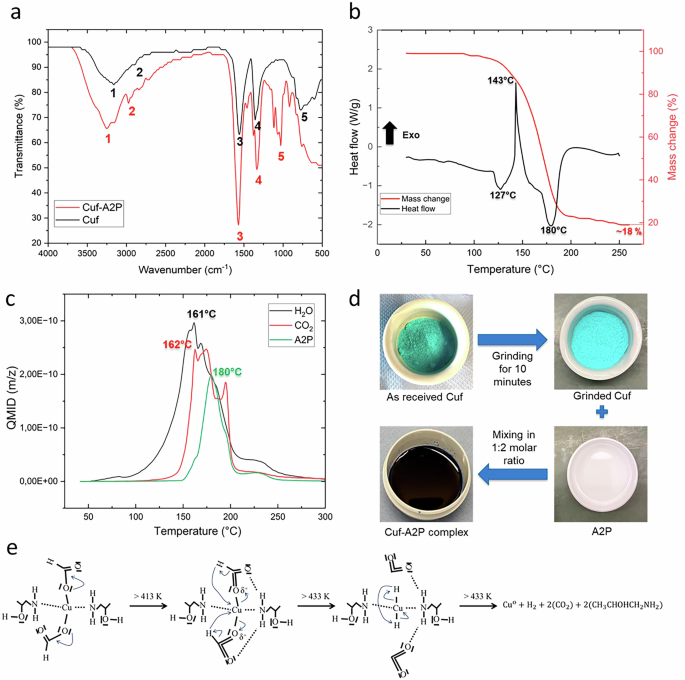
a Cuf-A2P complex (red) investigated for various chemical bonds present in it compared to Cuf (black) using FTIR. b DSC (black)—TGA (red) analysis of Cuf-A2P indicating various endothermic and exothermic reactions along with the mass loss taking place during the thermal decomposition of the Cu complex. c Corresponding MS of Cuf-A2P complex indicating the release of gaseous by-products during the thermal decomposition. d Synthesis of Cu-A2P complex. e Decomposition reaction mechanism of Cuf-A2P amine complex.
Figure 2b shows the DSC (black curve) and TGA (red curve) analysis of Cuf-A2P complex. Cuf-A2P complex decomposition consists of a dehydration step (endothermic peak at 127 °C) followed by decarboxylation (oxidation of formate ion) and Cu reduction reaction (Cu2+ → Cu1+ → Cu0), where CO2 and H2O are released as gaseous byproducts42. This exothermic reaction (decarboxylation reaction, peak at 143 °C) is followed by an endothermic reaction (peak at 180 °C), where evaporation of the released amine takes place. The final mass loss at 18 wt.% in TGA curve represents the amount of Cu (in wt.%) after the thermal decomposition process. The released by-products during the thermal decomposition of Cuf-A2P was further validated using mass-spectroscopy analysis (as shown in Fig. 2c). The Quasi Multiple Ion Detection (QMID) curve represents the ion current measured for specific molecules and evolved gas analysis using mass spectroscopy (MS). From the MS analysis, it is observed that H2O has evolved as early as 60 °C indicating the onset of dehydration step, which is in consensus with the DSC-TGA curve. The H2O peak is observed at around 161 °C indicating the release of H2O during the decarboxylation reaction. Similarly, CO2 peak is observed at around 162 °C (onset from 124 °C—in consensus with DSC-TGA curve) indicating the release of CO2 during the decarboxylation reaction42. The evaporation of the released amine starts after 150 °C, which is close to the boiling point of A2P (159 °C), and its peak is observed at around 180 °C which matches the endothermic peak as observed in the DSC curve. Overall, no further gaseous byproducts are observed after 250 °C, which aligns with no further mass loss observed in the TGA measurement. Additionally, a DTG-TGA curve has also been included in the supplementary data as Supplementary Fig. 1 to understand the rate of material loss over temperature. Figures 2d and 2e shows synthesis of Cuf-A2P complex and its subsequent decomposition reaction mechanism. The prepared Cuf-A2P complex has a Cu metal content of 16.95 wt.% and a viscosity of 600-650 mPas. For preparation of the Cu complex ink for inkjet printing and spray coating, viscosity in the range of 3–30 mPa.s are suitable for realize thin printed traces (<20 µm)61. Therefore, a mixture of ethanol (lowering the viscosity) and PEG600 (stabilizing agent) were added to Cuf-A2P complex as carrier solvent. The resulting Cu complex ink has a Cu metal content of 8.46 wt.% and a viscosity of 9.5 mPa.s. Contact angle of Cu complex ink on PET and polyimide were 61° and 42°, respectively. A contact angle in the range of 40°–50° is preferred for achieving an inkjet printed pattern with a good aspect ratio and resolution. In order to reduce the contact angle on PET substrate, Byk 333 (1 mL) was introduced as a surfactant to the Cu complex ink. The modified ink for PET substrate resulted in a contact angle of 44°, improving the ink wettability.
Laser processing window for Cu complex ink on polyimide and PET substrates
In order to fabricate dense and homogenous Cu metallic traces on polymeric substrates such as PET and polyimide, calculation of energy density plays a vital role in understanding the substrate-ink-laser interaction. Before laser sintering, the inkjet printed traces were then predried at 100 °C for 5 min under air to remove excess organics that can cause rapid degassing and inhomogeneous traces during sintering. For sintering using the continuous spot laser, energy density is the total energy delivered to the target material per unit area during the scanning process. The energy density should be high enough to decompose the Cu complex ink to generate Cu NPs and promote sintering, but not so high that it damages the underlying polymeric substrate. For this reason, determination of laser processing window using energy density is required to find a balance between sufficient sintering of Cu NPs and minimal thermal impact on the substrate. Energy density (ED) of a continuous wave laser during scanning can be calculated using laser power (P), scan rate (v) and laser spot diameter (d) as shown in the Eq. (1)62.
Using this formula, a processing window for different sintering regions (not sintered (NS)—blue, sintered (S)—green and substrate damage (SD)—red) for Cu complex ink on PET and polyimide substrates was realized (as shown in Fig. 3a). Table 2 gives an overview of corresponding threshold of energy densities for different sintering regions on PET and polyimide substrates.
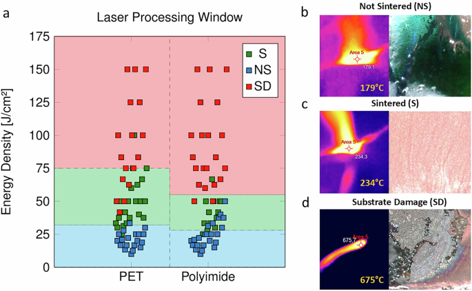
a Graphical representation of laser processing window for different sintering region using 60 sample points for both PET and polyimide. b Surface temperature of NS sample measured using thermal camera (left) and optical inspection of the sample showing not sintered Cu complex ink (right). c Surface temperature of S sample measured using thermal camera (left) and optical inspection of the sample showing a well sintered Cu layer (right). d Surface temperature of SD sample measured using thermal camera (left) and optical inspection of the sample showing ablated or damaged region (right).
A good sintering window for PET and polyimide substrates for a printed Cu complex ink thickness of 20 ± 3 µm is observed, when the energy density is between 30–75 J/cm² and 25–50 J/cm² respectively. In this process window, the predried Cu complex ink successfully decomposes and sinters without damaging the underlying polymeric substrate. However, few sample points (out of 120) do overlap the assigned sintering region, since they show a mixed sintering behavior. This is mainly attributed to the partly non-sintered or substrate damage regions observed in these samples due to variation in thickness of printed layer (±3 µm), indicating a sharp dependence on the printed layer thickness. This deviation can be reduced by assigning regular cleaning cycles after each printing pass. Both PET (0.01)63,64 and polyimide (0.001)65,66 have a very low absorbance for 1070 nm continuous laser compared to Cu complex ink (0.5)45, which can enable Cu sintering without damaging the substrate. An absorbance (OD) spectrum of Cu complex ink prepared for this experiment has also been included in the supplementary data as Supplementary Fig. 2 for reference. Polyimide (0.8–1.2 W/mK)67 also has comparatively higher thermal conductivity compared to PET (0.19 W/mK)68. In addition, the calculated thermal diffusivity of polyimide is 0.0055 cm2/s and for PET is 0.0012 cm2/s, which is also higher. This means that heat spreads faster in polyimide, leading to a narrower temperature range for effective sintering. If the laser energy is too low, the Cu ink won’t sinter sufficiently or if it’s too high, the heat will spread quickly, potentially damaging the polyimide substrate59. Additionally, PET is a thermoplastic (softens upon heating), and polyimide is a thermosetting plastic (remains hard when heated)69. Based on the nature of material, PET can withstand more localized heating before reaching a permanent damage whereas polyimide is susceptible to damage from excessive heat. Hence, a smaller working window is observed for polyimide compared to PET in Fig. 3a.
Based on the previous results, it is found that Cu NP formation in Cu complex begins at 130 °C followed by evaporation of A2P starting around 150 °C. In order to determine the surface temperature for different sintering regions, a thermal camera was installed to monitor the real-time temperature of the printed traces during the laser sintering. For NS sample (ED: 24 J/cm²), the temperature measured was 179 °C (Fig. 3b) which was insufficient to completely sinter the Cu complex ink, however some Cu formation can still be seen. For S sample (ED: 38 J/cm²), the surface temperature was measured at 234 °C (Fig. 3c), which resulted in well-sintered Cu layer. And for SD sample (ED: 75 J/cm²), the underlying polymeric substrate was already ablated or damaged due to very high surface temperature of 675 °C (Fig. 3c).
Impact of laser profile on sintered trace morphology
In addition to calculation of optimum energy density for achieving well sintered Cu layer, the sintered trace morphology is also dependent on the profile of the laser. Two commonly used laser profiles are Gaussian and top hat. In a Gaussian profile, the intensity of the laser beam is highest at the center and gradually decreases towards the edges70. It generates a spot with a non-uniform energy distribution. This may be beneficial for laser cutting or engraving processes, however in sintering it causes uneven heating—producing non-homogenous Cu layers with lower density71. On the other hand, a top hat or flat top profile has a uniform intensity across the beam, creating a uniform energy distribution70,71. This enables realization of homogenous and densely packed sintered layers or traces exhibiting consistent material properties. Two samples are laser sintered using Gaussian and top hat profile as shown in Fig. 4. For this experiment, a continuous spot laser with Gaussian profile (same as in previous section) and a continuous line laser with top-hat profile are used. In Fig. 4a, the intensity of laser beam for Gaussian profile at the edges is different compared to that at center—leading to difference in energy density. The excess energy at center lead to substrate damage since it is above the ablation threshold whereas at the edges formation of sintered Cu layer takes place (as seen in Fig. 4b—left). On the other hand, the laser intensity is uniform in case of top-hat profile leading to a homogenous energy density from edge to center (as seen in Fig. 4a). This enables an even heat distribution leading to formation of homogenous sintered Cu layer (as seen in Fig. 4b—right). Further, the SEM images of laser sintered samples using top-hat profile reveal a more uniform and densely packed microstructure compared to Gaussian profile, where a non-homogenous sintered structure is observed (as observed in Fig. 4c, d). This study also highlights a main difference in terms of laser optics used for sintering. The line beam optic allows a more uniform coverage over a larger area facilitating faster production speed but with high energy consumption. The spot optic offers higher precision and can fabricate intricate patterns with low energy consumption. Therefore, the selection of laser optics in printed electronics depends on specific application, desired precision, production speed and cost.
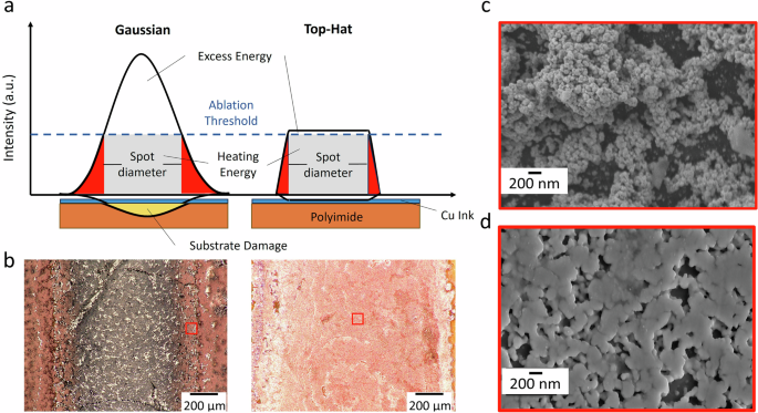
a Schematic of laser intensity distribution for Gaussian and top-hat profile and its energy distribution on sintering samples. b Optical inspection of laser sintered sample using a Gaussian profile showing substrate damage (left) and using top-hat profile showing a well sintered Cu metallic layer (right). c SEM image of sintered Cu layer using the continuous spot laser with Gaussian profile near the substrate damage area (red box on the left image of b) showing a non-homogenous sintered structure. d SEM image of sintered Cu layer using the continuous line beam laser with top-hat profile showing a uniform and densely packed Cu microstructure (red box on the right image of b).
Characterization of metallic Cu traces for printed electronics
The sintered Cu metallic traces for printed electronic application can be fabricated using two application methods as discussed earlier. Using method 1, a continuous-wave spot or line beam laser with a top-hat profile can be used to sinter the predried inkjet printed pattern, by traversing the laser over the printed layer. However, spot laser would require precise movement and positioning to accurately sinter the desired locations in intricate inkjet printed pattern of Cu complex ink. In addition, pattern design must be fed into the laser system using CAD (Computer-Aided Design) files that will help guide laser along the exact pattern. On the other hand, line beam laser reduces the time and complexity of stage or axis movement, achieving uniform sintering over larger areas but only through high energy consumption. Both of the laser optic configuration can be used on different layer thicknesses by varying the laser parameters to achieve a desired energy density and choice between them depends on specific application and desired outcome.
Using application method 2, a fine conductive Cu traces (width: ~90−100 µm) can be achieved using a continuous spot laser with beam diameter of 51 µm on uniform spray coated layer (~5 µm) of Cu complex ink. Spray coating method not only enabled printing of Cu ink layer of similar thickness as that of inkjet printed trace but also provided flexibility in terms of adjusting the viscosity of the ink. Since, thickness of the printed layer plays an important role in laser sintering, similar layer thicknesses were mandatory for both the processes to use similar laser parameters. This method enables direct patterning of metallic Cu circuitry using a CAD or image file on flexible polymeric substrates using the combination of galvanometer mirror scanner and laser beam. After the patterning process, the uncured Cu complex ink can be either reused or washed off using isopropanol in an ultrasonic bath. Analyzing both the methods reveal that if precise, fine features is desired outcome—method 2 might be advantageous. However, if the design is larger and less intricate, the uniform coverage and speed of line beam laser in method 1 can be beneficial.
To investigate the adhesion and electrical properties of the metallized Cu layer, method 2 was used to prepare the test samples. The Cu metallic traces showed good adhesion to polymeric substrates after performing the Tape Test (ASTM D3359)72. There was no peel off observed, indicating a rating of 5B (best adherence) on a scale of 0 to 5. Figure 5a and Fig. 5b show the SEM-topographic and SEM-FIB images of the sintered Cu traces onto the polymeric substrate. The topographic images show a dense sintered structure with visible sintered neck structures. A cross sectional analysis using the FIB shows that the thickness of the sintered Cu layer was about 0.7–1 µm. Using the average thickness (t) and the sheet resistance (Rs) measured using a 4-point probe, the bulk or volume resistivity (ρ) is calculated using equation (2)73.
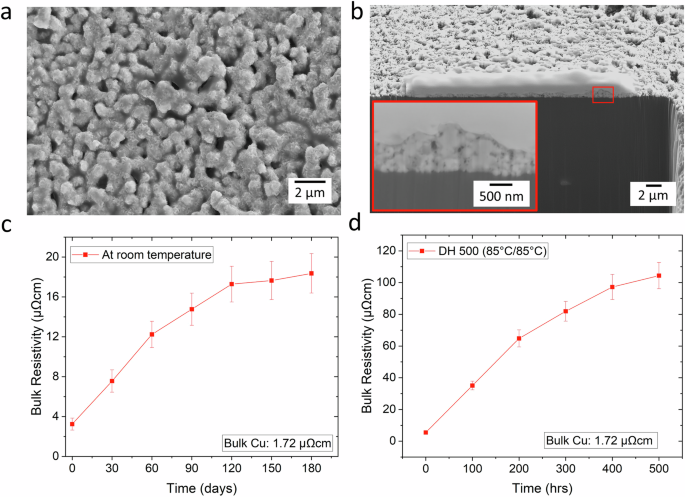
a SEM image: Topographic view of sintered Cu layer prepared using application method 2, showing a dense sintered structure with large necking. b SEM image: FIB cross section showing thickness of the sintered Cu layer with a magnified image indicated in the red region (Note: The thickness values have been corrected for the 52° tilt angle of the sample). c Variation of bulk resistivity with time (in days) after room temperature storage for 180 days. d Variation of bulk resistivity with time (in hours) after temperature—humidity storage (DH 500) at 85 °C-85% humidity for 500 h.
Alternatively, the bulk resistivity (ρ) can also be calculated using the Eq. 3, where R is the measured resistance and L, w, t are length, width and thickness of the sintered Cu trace73.
Figure 5c, d shows the measured bulk resistivity of sintered Cu traces under two conditions: after room temperature storage for 180 days and after temperature—humidity storage (DH 500) at 85 °C-85% humidity for 500 h respectively.
Cu has a bulk resistivity of 1.72 µΩcm, it is observed that at zero condition i.e., right after laser sintering (under air) the bulk resistivity of sintered Cu traces was 3.24 ± 0.6 µΩcm (1.87 times that of bulk Cu). Following the room temperature storage, the bulk resistivity of sintered Cu traces gradually increased from 3.24 ± 0.6 µΩcm (Day 0) to 17.28 ± 1.79 µΩcm (Day 120). Afterwards, the increase was slightly pronounced—measuring 18.36 ± 1.98 µΩcm after 180 days. This can be attributed to the passive oxide layer that has already formed on top of the metallized Cu over time. Additionally, temperature–humidity storage tests were also performed on the laser sintered Cu samples to evaluate the influence on bulk resistivity over time (hrs). The bulk resistivity of the samples gradually increased over time reaching 104.4 ± 8.3 µΩcm after 500 h. This necessitates the application of an encapsulation layer over the sintered Cu layers to prevent this gradual degradation. Further investigations are ongoing to develop an in-situ encapsulation mechanism within the Cu complex inks.
In conclusion, the study demonstrated remarkable aspects of utilizing Cuf as the Cu metal precursor and A2P as the complexing agent. The FTIR, DSC, TGA, and mass spectroscopy investigations delivered insightful analysis on the decomposition reaction of Cuf-A2P. The energy density and laser profiling in the sintering process was explicitly underlined. Continuous-wave laser, along with precise energy density calculation (30–75 J/cm² for PET and 25–50 J/cm² for polyimide), ensured effective sintering preventing any substrate damage. The adoption of a top-hat laser profile solidifies the approach, displaying an even energy distribution, which ultimately led to a homogeneous and densely packed Cu layer. Contrarily, the Gaussian profile presents non-uniform sintering due to non-uniform energy distribution. Despite notable findings, a critical aspect of degradation in bulk resistivity over time unfolded. The bulk resistivity rises from initial 3.24 µΩcm (at zero condition) to 18.36 µΩcm following a 180-day period under room temperature storage, indicating a nearly 467% increase. Further, temperature-humidity testing results in a dramatic increase in bulk resistivity to 104.4 µΩcm after 500 h, signaling an urgent need for an in-situ encapsulation mechanism within the Cu complex ink. In essence, the research highlights immense potential of Cuf-A2P complex inks in realizing printed electronics applications. However, the critical necessity for further research on optimizing the longevity of the sintered Cu layer by encapsulation is advised for its wide-scale applicability. The encapsulation could be done as for Printed circuit boards applying a resist for protection or adding polymer into the ink which is harden during sintering.
Methods
Materials
Cu (II) formate tetrahydrate (Cuf), (Cu(HCOO)2·4H2O, 98%, as received (AR)) was purchased from Thermo Fisher Scientific, USA. 1-Amino-2-propanol (A2P), (C3H9NO, 93%, AR) was purchased from Sigma-Aldrich, Germany. Ethanol (C2H6O, >96%, AR) and Polyethylene glycol 600 (PEG 600), ((C2H4O)n, >98.5%, AR) were purchased from Carl Roth, Germany. BYK-333, a silicon containing surfactant was obtained from BYK-Chemie GmbH, Germany. Polyimide films (Kapton® HPPST-125 µm) and PET films (Melinex® ST506/505-125 µm) for printing were obtained from DuPont, USA. These polymeric substrates are free of additives.
Preparation of Cu complex ink
A Cuf-A2P complex was prepared by mixing Cuf (6 g) and A2P (4.12 mL) in specific molar ratio of 1:2 based on our previous work42. Before mixing, the Cuf was finely ground using a mortar and pestle for 15 min. For preparation of the Cu complex ink for inkjet printing and coating purpose, ethanol (25.34 mL) and PEG600 (0.9 mL) were added to Cuf-A2P complex as carrier solvent. The viscosity of the Cuf-A2P complex and ink were measured using a viscometer (Thermo Scientific Haake TM Viscotester TM, USA). Subsequently, contact angle measurements of the Cu complex ink on both PET and polyimide substrates were conducted using a drop shape analyzer (Kruss DSA 30E, Germany).
Characterization of Cu complex ink
The thermal decomposition of the ink (heat flow and mass loss) was analyzed using differential scanning calorimetry (DSC 821 from Mettler Toledo, USA) and thermal gravimetric analysis (TGA/DSC 3+ from Mettler Toledo, USA). In addition to DSC and TGA, mass spectroscopy of the Cuf-A2P complex was carried out using QMS 403 Aeolos Quadro analyzer system from Netzsch, Germany. The samples were measured under a N2 atmosphere (flow rate: 30 L/min) with a heating rate of 10 °C/min up to 250 °C followed by an isothermal holding at 250 °C for 5 min. The particle morphology after decomposition was evaluated using a scanning electron microscope (Auriga 40 Crossbeam FIB/SEM, Zeiss, Germany). The Cuf and Cuf-A2P complex are investigated by Fourier transform infrared spectroscopy (FTIR, Spotlight 200 ATR-FTIR from PerkinElmer, USA) with the attenuated total reflection (ATR) technique for evaluation of absorption band of various organic bonds.
Application method 1: inkjet printing and fabrication of conductive Cu traces
In the first method, the Cu complex inks were inkjet printed using a Dimatix Materials Printer (DMP-2850, Fujifilm Dimatix Inc., USA) onto the PET and polyimide substrates. The inkjet printing parameters (drop spacing: 20 µm, jetting voltage: 40 V, no. of layers: 10, frequency: 80 kHz, printhead type: SambaTM, no. of nozzles used: 8) were used to realize the printed Cu complex ink traces. Before printing, Ar-plasma treatment of the PET and polyimide substrates were carried out to remove organic residues from the surface for 5 min (Zepto PLS, Diener electronic, Germany). The printed traces were then predried at 100 °C for 5 min under air to remove excess organics that may cause rapid degassing and inhomogeneous traces after sintering. The predried traces were then laser sintered using a continuous-wave infrared (1070 nm) spot laser (JK400FL) from GSI group, UK and line beam (360 W T-SPOLD, optic size: 2 mm × 80 mm, wavelength: 940 nm) laser from Hamamatsu Photonics Deutschland GmbH, Japan. The continuous-wave spot laser beam was focused on the sample placed on three-axis automatic table (Aerotech Ltd, UK) with a focal lens of 125 mm focal length (Thorlabs, Germany). The raw and focused laser beam diameter were 6.0 mm and 32.0 µm, respectively. The analysis of processing window for sintered samples (not sintered, sintered, substrate damage) on PET and polyimide substrates was performed using the spot laser. Table 3 shows the laser and material parameters used to evaluate energy densities for different sintering regions. Additionally, a thermal camera was used to measure the surface temperature of the sintered traces to evaluate the temperature threshold for good sintering.
Application method 2: spray coating and fabrication of conductive Cu traces
In the second method, the Cu complex inks were spray coated onto the polymeric substrates using a spray coating head (Air atomizing spray valve system SV-6) and digital control spray controller (Spray Master) from Musashi Engineering Inc, Japan. Using the process settings (nozzle diameter: 100 µm, spraying distance: 500 µm, syringe (Tank) pressure: 3 kPa, nozzle pressure: 45 kPa), a uniform film thickness of ~5 µm was achieved. A similar surface pretreatment and predrying process was used for spray coated samples as well. The laser sintering was performed using infrared (1064 nm) spot laser (G3 20 W nanosecond pulsed spot laser) supplied by SPI Laser, UK. The spot laser can work in continuous-wave and pulsed (from 9 ns to 200 ns) with 22 W as maximum power. The beam quality and transverse electromagnetic mode were 2.1 and 00, correlatively. The raw laser beam diameter was expanded at 5.77 µm with manual beam expander (Linos, 2-8x, Qioptiq, Germany). The expanded laser beam was addressed to the galvanometer mirror scanner (Nutfield Extreme-15-YAG, Germany) controlled using SAMLight v3.05 software (SCAPS Gmbh, Germany). The galvanometer mirror scanner allows to move the laser beam with speeds from 0.01 mm/s to 20,000 mm/s. After the galvanometer mirror scanner, the laser beam was focused at 51 µm with focal lens of 100 mm (Linos Ronar F-Theta focal lens, UK). The samples were placed on the 3 axis automatic table (Aerotech Limited, UK).
Characterization and reliability investigation of sintered Cu traces
The optical inspection of the laser sintered traces were analyzed using an optical microscope (Keyence VHX-900F 3D microscope, Japan). The morphology and cross section investigation using focused ion beam milling were evaluated using a scanning electron microscope (Versa 3D DualBeam FEG FIB-SEM, Thermo Fisher Scientific, USA). An optical light profilometer (Nanofocus µ-surf, Germany) was used to measure the thickness (after printing and sintering) and roughness of the sintered traces. The bulk resistivity (ρ) of the metallic Cu trace was calculated from the thickness of the trace (t) and sheet resistance (Rs) measured using a 4-point probe (Keithley 2461, USA). The fabricated Cu sintered traces were also used for the reliability investigations carried out in a temperature-humidity chamber (CTC-256 from Memmert, Germany; DH500 (85 °C, 85% humidity) to check their electrical performance. Subsequently, a standard Tape Test (ASTM D3359) is performed using a pressure sensitive adhesive tape (3 M) to evaluate the adhesion quality of the laser sintered traces.


Responses