Mapping the energy-momentum dispersion of hBN excitons and hybrid plasmons in hBN-WSe2 heterostructures
Introduction
Van der Waals (vdW) heterostructures formed by stacks of two-dimensional (2D) layers1 have attracted a lot of attention due to the possibility of creating materials with customisable physical and chemical properties2,3. Much of the recent research has been devoted to identifying new material combinations4,5,6,7,8 and investigating their electronic and optical properties both, theoretically9,10,11,12,13,14,15,16 and experimentally17,18. Transition metal dichalcogenides (TMDCs) and TMDC-based vdW heterostructures have gained increasing attention due to their rich excitonic and plasmonic landscapes19,20,21. Hexagonal boron nitride (hBN) is a prominent encapsulant for nanoelectronics and nanodevice fabrication22,23,24 as it is thought not to perturb the properties of the TMDCs thanks to its insulating character. Encapsulation with hBN has also been adopted as a reliable method to decrease the excitonic bandwidth in TMDCs and increase the overall intensity of the excitonic signal25,26. This has been related to the suppression of detrimental environmental factors such as absorption of oxygen and moisture25,26. Due to the presence of strong excitonic resonances in the ultraviolet (UV) spectrum of hBN (5.2 – 6.3 eV), it has also been studied in the field of deep UV plasmonics27,28.
The presence of intense excitons in the response of hBN raises questions regarding their effect when hBN is combined with TMDCs. For instance, a minor but consistent shift in energy has been reported for the A and B excitons in TMDCs when combined with hBN25,29. Moreover, little is known about if and how plasmon modes and higher energy excitons in TMDCs and hBN interplay when stacked. A major difficulty is that excitonic and plasmonic resonances are known to exhibit a very different energy-momentum dispersion relation which requires that a broad range of both, momentum and energy are considered in experiments. Also, the large momentum makes excitons in hBN unsuitable to be probed by optical methods. Finally, less explored anisotropic effects in the excitons have been shown in hBN using inelastic X-ray scattering measurements30. All these factors make the study of hBN-TMDCs heterostructures particularly challenging.
In the last decade, electron energy-loss spectroscopy (EELS) has become an increasingly powerful technique to investigate a wide range of phenomena due to its unique combination of energy, spatial, and momentum resolution and range31,32,33. It has been successfully employed to study TMDC excitons while focusing on the lower energy A and B excitons in individual layers34,35,36, in twisted bilayers34 as well as combined with graphene or hBN37,38. A less explored aspect is that EELS can be employed to study an energy range of several electronvolts and a momentum range of several Brillouin zones (BZs) in a single acquisition39. The latter provides access to the higher energy excitons in TMDCs40. So far, EELS has also successfully been employed to study the characteristic plasmon modes41, their interplay with excitons35, as well as their dispersion42 in individual 2D materials. The plasmon energy-momentum dispersion of bulk hBN has been studied using EELS for decades43,44. Recent interest in this material, both, in its few-layer form and in combination with TMDCs45,46, has revived interest and led to new studies with improved accuracy47,48,49. To our knowledge, no EELS research on higher energy excitons and plasmons in TMDC-hBN heterostructures has been reported on. In parallel, ab initio methods based on density-functional theory (DFT) and its time-dependent extension (TDDFT) have contributed considerably to extending our understanding of the fundamental properties of (complex) materials, including their response to radiation with finite momentum transfer50,51,52.
Here, we present a joint experimental and theoretical study to explore the response of WSe2, hBN and their multi-layer heterostructures in the energy range 1–38 eV. Momentum-resolved EELS (q-EELS) was employed to generate energy-momentum (ωq) maps of hBN, WSe2 and their stacks to study plasmons and excitons. TDDFT calculations of the q-dependent loss function of the individual building blocks showed excellent agreement with the experiments regarding the main plasmon resonances and their energy-momentum dispersion at increasing momentum transfer along the high symmetry directions of the lattice. We found that combining hBN with WSe2 leads to hybridisation of the main bulk plasmon resonance resulting in changes to its energy and dispersion in the heterostructure. Energy-momentum maps revealed the complex dispersion at high-q of the excitons of hBN alone, which was largely retained when combined with WSe2. Surprisingly, the peaks associated with higher energy excitons originating in the WSe2 layer of the WSe2-hBN heterostructure showed the best agreement with the signatures of monolayer WSe2 and not as expected with the few-layer WSe2 of the same thickness. The consequences of using hBN to encapsulate TMDCs are also discussed.
Results
The interactions probed in the present work are schematically summarised in Fig. 1a. The possible hybridisation of plasmons and excitons originating from the WSe2 and the hBN layers in their heterostructure was analysed using q-EELS. In conventional EELS, a circular aperture is placed in the diffraction plane before the spectrometer, resulting in a loss spectrum that is averaged over several BZs and thereby losing momentum information. To retain the momentum information, a slit aperture can be placed into the diffraction plane after the sample (Fig. 1a). By aligning this slit to the high symmetry directions of the BZ (Γ → K and Γ → M, see Fig. 1b), it is possible to record a dispersion diagram in parallel as shown in Fig. 1a.
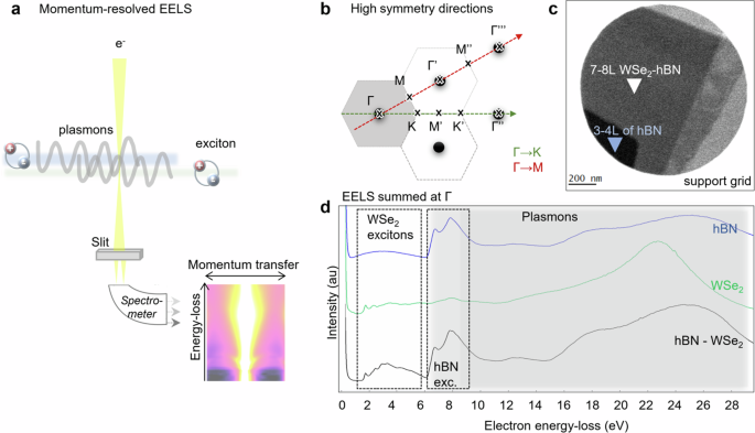
a Schematic of the hBN-WSe2 heterostructure investigated using momentum-resolved EELS (q-EELS). Excitons and plasmons and their coupling were studied by placing a slit before the spectrometer in the high symmetry directions Γ → K and Γ → M to select energy-loss spectra while retaining the momentum information. b Schematic of the k-space showing the directions of high symmetry, Γ → K and Γ → M. c Image of the regions of interest showing the WSe2-hBN heterostructure and the hBN. The thickness was found to be 7–8 layers for the heterostructure, with the hBN accounting for 3–4 layers. d q-EEL spectra for electrons with zero momentum transfer (q = 0) for hBN (blue spectrum), WSe2 (green spectrum), and WSe2-hBN (black spectrum) showing the loss regions associated with excitons from WSe2 and hBN as well as the energy-loss region associated with the plasmons (shaded grey).
The high-angle annular dark field (HAADF) image presented in Fig. 1c shows the region of interest. The thickness of the heterostructure was found to be approximately 7–8 layers in total, with the hBN accounting for 3–4 layers (using conventional EELS thickness measurements). Next, q-EELS maps were acquired of hBN and the hBN-WSe2 heterostructure, as well as a reference region of WSe2 of similar thickness as found in the heterostructure. Using q-EELS, it is possible to compare the energy-loss spectra for electrons with zero momentum transfer (q = 0), as shown in Fig. 1d. The signature peaks associated with the different materials can be observed in the q-EEL spectra for hBN (blue), WSe2 (green), and their heterostructure (black). In hBN, there are characteristic exciton losses between 5.5 eV and 9 eV (Fig. 1d boxed region). While for WSe2 there are peaks associated with excitons in the lower energy-loss region from 1.6 eV (Fig. 1d boxed regions). The characteristic main plasmon loss region for both materials is found between ~8 eV and ~28 eV (Fig. 1d shaded in grey). On first inspection, the q-EEL spectrum for the heterostructure appears to be a combination of both of its components, with excitons from WSe2 and hBN as well as plasmons from WSe2 and hBN contributing to the overall spectrum. This interpretation turned out to be inaccurate once we compared the spectra for varying |q|.
Plasmon dispersion in hBN and WSe2
The energy-momentum dispersion of plasmons and excitons was studied in the q-EEL spectra for a momentum transfer between q = 0 and |qmax | = 0.5 × |Γ − Γ′| (midpoint between Γ and Γ′ in direction Γ → M) and between q = 0 and |qmax | = 0.5 × |Γ − Γ′′| (midpoint between Γ and Γ′′ in direction Γ → K) (see Fig. 1b). A larger range in momentum transfer, covering at least an entire BZ, is frequently shown to demonstrate an absence of artifacts.
The ωq maps of hBN show the energy-momentum dispersion of 3–4 layers (3–4 L) of hBN in the Γ → M (Fig. 2a) and in the Γ → K directions (Fig. 2d) with detailed fine structure. They show the dispersion of both, π (white arrow) and π + σ plasmon peaks43,53 from the centre of one BZ to the centre of the next BZ. When analysing the q-EEL spectra of hBN with different momentum transfer (Fig. 2c, f), these two plasmon peaks dominate the spectra. Both, the π (white arrow) and the π + σ plasmon peaks shift to higher energy losses with increasing |q|. The shift is more pronounced for the π plasmon peak as the π + σ plasmon peak is significantly broader and thus less well-defined. These energy-momentum dispersion behaviours are expected since the π + σ resonance is influenced by the contributions from both, π and σ bands leading to a hybrid, complex energy-momentum dispersion. Remarkably, both peaks remain detectable across the BZ despite the rapid fall in spectral intensity with increasing |q| [see Supplementary Information (SI) Supplementary Fig. 7]. The plasmon peaks exhibit a slightly different dispersion behaviour in the Γ → M direction compared to Γ → K. Along Γ → M, the π resonance is shifted from 7.8 eV at q = 0 to 12.3 eV for |qmax| (midpoint between Γ and Γ′ and the boundary of the first BZ) with a double shoulder with maxima at 12.25 eV and 12.75 eV at q ≈ 0 (Fig. 2c, green arrow). The fine structure of the double peak on the higher energy side of the π peak at q = 0 has been allocated by Arnaud et al.54 to π → σ∗ interband transitions using the GW method. The π + σ plasmon peak for q = 0 is at 25.6 eV with a shoulder at 17.6 eV. This feature has also been attributed to interband transitions by Arnaud et al.54. The π + σ resonance shifts to 30.4 eV for |qmax|. Along Γ → K, the π peak is shifted from 7.8 eV at q = 0 to 12.3 eV at |qmax| with a double-peak shoulder which rapidly vanishes with increasing |q | (Fig. 2f, green arrow). The π + σ resonance shifts from 25.6 eV at q = 0 to 30.3 eV at |qmax| with a shoulder peaked at 24.7 eV and 18.7 eV. This complex dispersion behaviour of the main plasmon peaks agrees with results obtained from non-resonant inelastic x-ray scattering30,47. The experimental values are summarised in Table 1.
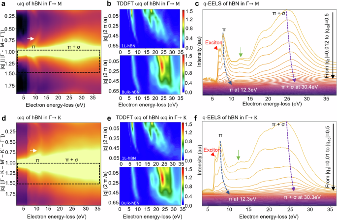
a Energy-momentum (ωq) map (log scale) of hBN in Γ → M showing the dispersion of both, π (white arrow) and π + σ plasmon peaks across the Brillouin Zone (BZ). b TDDFT maps of the energy-momentum dispersion of the main plasmon peaks along Γ → M for hBN showing quantitative agreement with experiments. c q-EEL spectra as extracted from a (boxed region) show that the π and π + σ peaks shift to higher energies with increasing |q| (up to |qmax| = 0.5 × |Γ − Γ′|). d ωq map (log scale) of hBN in Γ → K direction showing the dispersion of both, π (white arrow) and π + σ plasmon peaks across the BZ. e TDDFT maps of energy-momentum dispersion relations of plasmon peaks for hBN along Γ → K showing quantitative agreement with experiments. f The q-EEL spectra as extracted from a (boxed region) show that the π and π + σ peaks shift to higher energies with increasing |q| (up to |qmax| = 0.5 × |Γ − Γ’′|).
These experimental results were complemented by TDDFT calculations of hBN (details in the methods section). This methodology has known limitations in describing excitons in solids55. Bethe-Salpeter equation represents a more reliable alternative and corresponding q-dependent implementations are currently available in several codes56,57. They are, however, too computationally expensive to be applied on the heterostructures and energy range considered in our experiments. In the following analysis, we focus on the plasmonic response of the systems which can be reliably described with TDDFT58,59. The q-dependent loss function, given by L(q,ω) = −Imε−1(q,ω), where ε is the macroscopic dielectric function of the material, was calculated at finite values of transferred momentum in the two in-plane directions Γ → M (Fig. 2b) and Γ → K (Fig. 2e). The direction of transferred momentum was assumed to be the x-axis such that only the qx component was varied from 0.01 (2π/a) to 0.61(2π/a). The dispersion behaviour of the π + σ plasmon peak of hBN was found to be highly dependent on thickness and a detailed analysis of this thickness effect can be found in the Supplementary Figs. 1 and 3. Specifically, it was found that the π + σ plasmon peak exhibits the largest q-dependent shift in monolayer hBN (shown in Fig. 2b) in comparison to the bulk hBN (shown in Fig. 2e). The computational energy-momentum dispersion relations for 3 layer hBN agree with the experimental results in the 3–4 layer hBN sample regarding the shifts of the main plasmon peaks. Computationally, the π plasmon resonance is featured at 6.7 eV for q = 0.01, while for |qmax| it shifts up to 10.3 eV along Γ → M and to 10.1 eV along Γ → K. The π + σ plasmon peak is found at 19.2 eV for q = 0.01 and shifts to 24.2 eV at |qmax| along Γ → M and to 23.6 eV at |qmax| along Γ → K. These findings show quantitative agreement between calculations and experiments concerning the plasmon shifts.
The ωq maps of WSe2 show the energy-momentum dispersion in the Γ → M (Fig. 3a) and in the Γ → K directions (Fig. 3d) with great fine structure detail. The dispersion of both, π and π + σ plasmon peaks from across one entire BZ are shown. The q-EEL spectrum in Fig. 3c shows a small shift of the π and π + σ peaks to higher energies with increasing |q| (up to |qmax| = 0.5 × |Γ − Γ′|). The plasmon peaks exhibit a similar dispersion behaviour in both directions. For q = 0, the π peak is found at 7.9 eV with a slight shoulder present at ≈10 eV, and the π + σ plasmon peak is at 22.8 eV. Contrary to hBN, the plasmon peaks exhibit the same dispersion behaviour in both directions, Γ → M and Γ → K. At |qmax| in Γ → M, a peak is observed at ≈10.4 eV, which most likely corresponds to the π peak, while the π + σ plasmon peak is shifted to 25.2 eV. In Γ → K, a small peak is present at 10.2 eV for |q| = 0.33 × |Γ−Γ′|, which vanishes for larger q and is no longer detectable at |qmax| . The π + σ plasmon peak remains detectable across the BZ and shifts from 22.8 eV at q = 0 to 24 eV for |qmax| = 0.5 × |Γ−Γ′|. It is worth noting that the response of WSe2 appears to be largely isotropic, which is in agreement with other studies of plasmons in TMDCs35,42,60. In contrast, but in agreement with Galambosi et al.30, hBN appears to exhibit anisotropy in the plasmonic response.
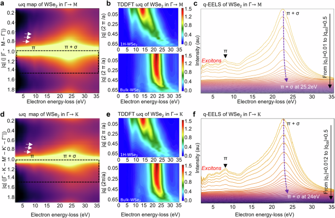
a Energy-momentum (ωq) map (log scale) of WSe2 along Γ → M showing the dispersion of the main plasmon peaks across the Brillouin zone (BZ). The π plasmon peak is denoted with white arrows. b TDDFT maps of the energy-momentum dispersion relations for WSe2 showing quantitative agreement with experiments. c The q-EEL spectra as extracted from a (boxed region) show very small plasmon shifts of π and π + σ peaks to higher energies with increasing |q| . d ωq map (log scale) of WSe2 in Γ → K direction showing the dispersion of the main plasmon peaks across the BZ. e TDDFT maps of the energy-momentum dispersion relations for WSe2 showing good agreement with the experiment. f The q-EEL spectra as extracted from a (boxed region) show how the main plasmon peaks shift to higher energies with increasing |q| . The π peak vanishes for |q| > 0.33 × |Γ − Γ′|, while the π + σ peak remains detectable across the BZ.
The computational spectrum of the monolayer and bulk WSe2 is also characterised by two resonances as shown in Fig. 3b, e, which are associated with the π and π + σ plasmons. Again, the effect of thickness was investigated computationally (details in the Supplementary Figs. 2 and 4). Since the π peak lies at the lowest boundary of the explored region, this feature is hardly distinguishable from the onset at 5 eV for multi-layer WSe2. Still, a trend of decreasing intensity with increasing q can be noticed even in the bulk sample. The π + σ plasmon peak is much stronger and broader, and its maximum is centred between 14.8–22 eV (depending on thickness) for q = 0. Since the thickness of the WSe2 sample was estimated to be 3–5 layers, the experimental results are best compared to the TDDFT maps for the 4 L structure. In this system, the π + σ plasmon peak is found at 17.1 eV for q = 0 with a low-energy shoulder visible at ≈12 eV. As for hBN, the peak intensity decreases with increasing transferred momentum, and this behaviour is accompanied by a shift of the peak to 25.8 eV along Γ → M and to 25.5 eV along Γ → K for large q. Overall, the energy shift is 8.4–8.7 eV for q > 0.45(2π/a). It is worth noting that for larger values of q, the low-energy shoulder remains almost constant in energy and disappears with q > 0.45(2π/a). Again, there is good agreement between the experiments and calculations in the qualitative behaviour, but the experimentally detected shift is smaller compared to the calculations.
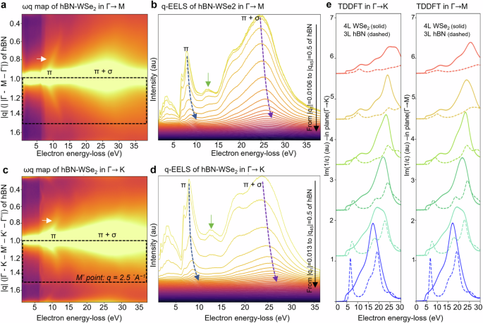
a Energy-momentum (ωq) map (log scale) of WSe2-hBN in Γ → M shows the dispersion of both, π (white arrow) and π + σ plasmon peaks across the Brillouin Zone (BZ). b The q-EEL spectra, as extracted from a (boxed region), show that the π and π + σ peaks shift to higher energies with increasing |q| (up to |qmax| = 0.5 × |Γ − Γ′|). c ωq map (log scale) of WSe2-hBN in Γ → K shows the dispersion of both, π (white arrow) and π + σ plasmon peaks across the BZ. d The q-EEL spectra, as extracted from a (boxed region), show that the π and π + σ peaks shift to higher energies with increasing |q| (up to |qmax| = 0.5 × |Γ−Γ′′|). e Overlaid TDDFT spectra as a guide to locate the main plasmon peak in the energy-momentum space for 4-layer (4L) WSe2 (solid) and 3-layer (3L) hBN (dashed). (Legend: blue: q = 0.01 (2π/a), turquoise: q = 0.09 (2π/a), green: q = 0.17 (2π/a), light green: q = 0.29 (2π/a), yellow: q = 0.45 (2π/a), red: q = 0.61 (2π/a).).
Plasmon hybridisation in WSe2-hBN heterostructure
The WSe2-hBN heterostructure (shown in Fig. 1c) was investigated using the same experimental approach adopted for the individual constituents. The ωq maps of WSe2-hBN along Γ → M (Fig. 4a) and along Γ → K (Fig. 4 c) show the energy-momentum dispersion of the main plasmon and exciton peaks with great structure detail. On first inspection, many major features of the ωq maps of hBN are retained for the heterostructure; however, some small changes appear. There is a prominent π peak centred at 7.86 eV for q = 0. The energy-loss position is close to the π peak positions of both, hBN (7.8 eV) and WSe2 (7.9 eV). An additional fine structure detail in the peak is discussed in section 1.3. Similarly to the hBN sample, a double peak appears as a shoulder in the heterostructure as well (see Fig. 4b, d, green arrows). These peaks are shifted in energies to 12.4 eV and 12.9 eV, in contrast to the values of 12.2 eV and 12.7 eV at q = 0 in hBN alone. In the heterostructure, the π peak shifts to 12.3 eV at |qmax| = 0.5 × |Γ − Γ′′| along Γ → K and to 12.2 eV at |qmax| = 0.5 × |Γ − Γ′| in the direction Γ → M. As in hBN alone, for q = 0 there is a shoulder but again it is slightly shifted to 17.3 eV. The main feature at q = 0 is the broad π + σ plasmon peak at 24.6 eV, which shifts to 31.15 eV for |qmax| in the Γ → K direction. At |q| = 0.22 × |Γ − Γ′′| the main π + σ plasmon peak appears to be composed of two peaks centred at 26.45 eV and at 28.64 eV with the lower energy peak vanishing for larger q. Neither peak corresponds exactly in energy to those in the individual components of the heterostructure at finite |q|. In contrast, along Γ → M, the π + σ plasmon peak shifts to 29.7 eV at |qmax|. As in the Γ → K direction, a second feature is absent at lower q. Furthermore, the fitting as shown in Supplementary Fig. 6 indicated no significant broadening of the peaks in the heterostructure. Hence, the dispersion of the hybrid π + σ plasmon lies between the values expected for either of its components. In the heterostructure, the main π + σ peak is found 1 eV lower in energy compared to the hBN and 1.8 eV higher compared to the WSe2.
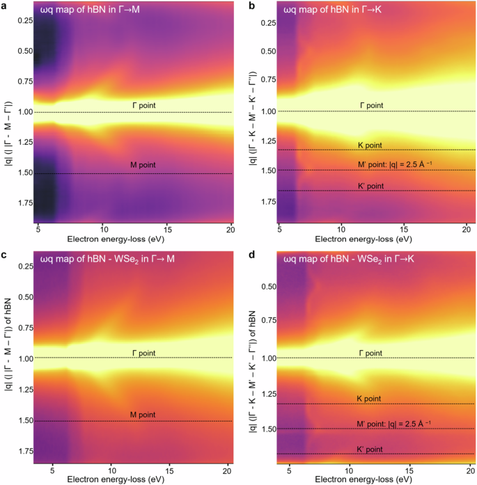
Energy-momentum dispersion (ωq) maps (log scale) of hBN show the signature of hBN excitons across the whole Brillouin zone (BZ). Fine structure details differ when comparing signatures at a the M point in the Γ → M direction and b the M’ point in the Γ → K direction. The same variations are present in WSe2-hBN when comparing the fine structure at c the M point in the Γ → M direction and d the M’ point in the Γ → K direction. A strong enhancement of the excitonic effects is observed between the K and M’ points in Γ → K direction for hBN and WSe2-hBN.
To compare the computational with the experimental values for the q-dependent loss function of the WSe2-hBN heterostructure, we overlay the results computed for the individual components assuming a stack of a tetralayer of WSe2 and a trilayer hBN. This serves as a guide to compare the energy-momentum landscape of both materials (see Fig. 4e). Comparing this to our experimental data of the actual heterostructure (see Fig. 4b, d), we found no match regarding energies or dispersion. The discrepancy between overlaid spectra and our experimental results highlights that there is a hybridisation of the plasmonic modes as observed experimentally and described above.
Effects of stacking on excitons
Lastly, the excitons and their possible hybridisation were investigated in the WSe2-hBN heterostructure. Using the combination of powerful EELS instrumentation and direct detector technology, we were able to map with great detail the complete energy-momentum dispersion of the high-momentum excitons in hBN and in the WSe2-hBN heterostructure; these results are presented in the maps shown in Fig. 5 as well as the spectra shown in Fig. 6a, c and 6b, d. In Fig. 6a–d, spectra obtained for small |q| are omitted from the graph due to the difference in spectral intensity causing the fine structure for finite |q| to get swamped (see Supplementary Figs. 7 and 8 for more details). Here, only the spectra from |q | = 0.15 × |Γ − Γ′| in direction Γ → M and from |q | = 0.05 × |Γ − Γ′′| in direction Γ → K are shown.
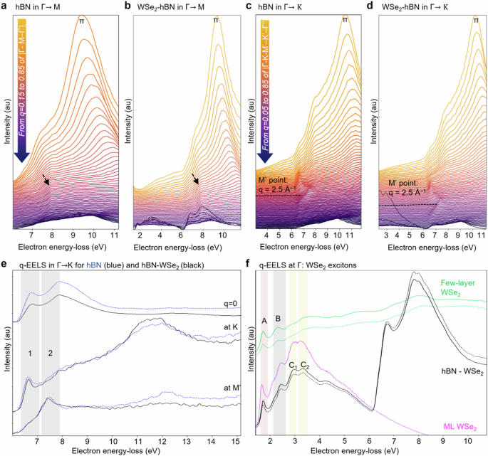
Individual spectra are shown for q from |q| = 0.15 × |Γ − Γ′| to |q| = 0.85 × |Γ − Γ′| (of the hBN lattice) in the Γ → M direction for a hBN and b the WSe2-hBN heterostructure. Individual spectra are shown for q from |q| = 0.05 × |Γ−Γ′| to |q| = 0.85 × |Γ − Γ′′| (of the hBN lattice) in the Γ → K direction for c hBN and d the WSe2-hBN heterostructure. e Overlaid spectra for q = 0 and at K and M’ point of both, hBN and WSe2-hBN heterostructure show the spectral shape redistribution for the excitonic peaks originating from hBN (denoted by ‘1’ and ‘2’). f The q-EEL spectra acquired at Γ (q = 0) for multi-layer WSe2 (solid line for the structure used here and dashed line for a reference of multi-layer WSe2 with an increased thickness) and WSe2-hBN heterostructure (solid line for the structure used here and dashed line for a reference of WSe2-hBN with an increased thickness) as well as a reference spectra for a monolayer WSe2 show changes in the peak position and relative intensity of higher energy WSe2 excitons, including in the B exciton region (grey shaded region) and C exciton region (yellow shaded regions). Only the A exciton peak (light red shaded region) exhibits a slight shift when compared to the reference monolayer WSe2 (pink spectra). The spectra are offset vertically for clarity.
The anisotropy of the excitonic dispersion in hBN becomes apparent when comparing the signal along Γ → M and Γ → K, as shown in the maps in Fig. 5a, b and in the spectra in Fig. 6a, c, respectively. For q = 0, there is an excitonic peak at 6.67 eV (see Fig. 6e, denoted by ‘1’) which has been identified using BSE calculations54,61,62. Additionally, it was reported in ref. 62 that this exciton is tightly confined within the layers of hBN, which ensures its robustness regardless of the stacking arrangement of hBN. At finite |q| in the Γ → M direction, only a shoulder just below 8 eV (black arrow) is visible for both, hBN and the heterostructure, as shown in Fig. 5a, c as well as Fig. 6a, b. Our findings agree with the BSE calculations from ref. 47, confirming the excitonic origin of this maximum. At q = 0, this peak overlaps with the π plasmon resonance and appears to contribute to it, giving rise to a lower energy shoulder (see spectrum at q = 0 in Fig. 6e).
In the Γ → K direction, there is a noticeable peak at 7.4 eV, which appears only at M’ as shown in Fig. 5b, d and Fig. 6c, d as well as in the overlaid spectra from the M’ point in Fig. 6e (denoted by ‘2’). This peak is assigned an excitonic character since it is reproduced in BSE calculations30,47. Furthermore, starting from the K point in the Γ → K direction, the lower energy peak appears to increase in intensity (see Fig. 6e, denoted by ‘1’). This strong enhancement of the excitonic effects can be observed between the K and M’ points for both, hBN (Fig. 5a, b) and the WSe2-hBN heterostructure (Fig. 5c, d). The pronounced excitonic intensities at M’ and K leading to a spectral shape redistribution were predicted by Fugallo et al.47. In their study however, the spectral enhancement was predicted at M and M’, while experimentally we find it only around M’. In our study, the distinct fine structure detail as described above is absent in the Γ → M direction (Fig. 6a) for both, hBN and the WSe2-hBN heterostructure (see Fig. 6b, d as well as Fig. 5c, d).
Next, we analysed the excitons originating in the WSe2 layer of the heterostructure by comparing the q-EEL spectra at q = 0 (Γ point). As the TMDC excitons have a very small dispersion40, it is reasonable to expect them to not overlap with other signals occurring at higher energy or higher momentum transfer. The q-EELS of WSe2 alone are shown for the same thickness of this component in the heterostructure (Fig. 6f solid green spectra) as well as for a thicker multi-layer WSe2 (Fig. 6 dashed green spectra) to assess the effect of thickness. For thinner WSe2, the q = 0 spectra are dominated by exciton rather than plasmon peaks. This behaviour reverses rapidly at increasing q (see Supplementary Fig. 8). The q-EELS of WSe2-hBN are shown for the same heterostructure as analysed previously (Fig. 6f solid black spectra) as well as for a thicker WSe2-hBN heterostructure for reference (Fig. 6f dashed black spectra). In the latter case, the thickness of only the hBN component was increased in the thicker WSe2-hBN heterostructure to assess the effect of hBN thickness, as hBN thickness is most commonly not accounted for when used for embedding. We found variations in relative peak intensities, but no detectable spectral differences regarding peak positions when varying the hBN thickness. In the literature, there is currently only agreement on the peak assignment of the A exciton in the EELS, but not on the higher energy peaks. Therefore, we acquired q-EEL reference spectra of monolayer and multi-layer WSe2 alone (see Fig. 6f as well as Supplementary Fig. 9). The EEL spectra show the energy-loss peaks associated with the excitons and their Rydberg state excitons for zero momentum transfer (|q| = 0). Detailed band structure calculations for monolayer WSe2 are available in the literature and we refer to them63,64 for the interpretation of the spectra.
In WSe2, the A and B excitons originate from a valence band splitting which has been calculated to be 0.4 eV in monolayer WSe265. As shown in Fig. 6f, there is a close agreement between the monolayer and the multi-layer WSe2 in the peak position of the A exciton, but not of the B and C excitons (further information is available in Supplementary Fig. 9). This is not surprising, as Hong et al.64 showed that in monolayer WSe2, the A’ Rydberg state and the B exciton peaks overlap, making the peak assignment non-trivial. In the same study, the third peak, frequently called C0 exciton, was proposed to be a B’ 2s-Rydberg state. The peak assignment becomes even more complex when considering that the Rydberg exciton states are expected to shift with the sample thickness to lower energy-loss positions66. Since there is no general consensus, we identified the excitons originating in the WSe2 as proposed by Hong et al.64.
Remarkably, the q-EELS of both, the thinner and thicker heterostructures (Fig. 6f, black dashed and solid spectra) are in close agreement with the q-EELS of the reference monolayer. Only the energy of the A exciton is shifted by 0.10 eV from 1.65 eV in monolayer WSe2 to 1.75 eV in the heterostructure (Supplementary Fig. 9), in line with previous observations25,29. There is excellent agreement in the spectral positions of the higher energy peaks. In the monolayer and the heterostructures, the B exciton is found at 2.15 eV (with the A’ Rydberg state expected at ≈2.08 eV). The third peak originates from the B’ 2s-Rydberg state (2.43 eV), which has also been identified as C0 peak. Higher energy peaks due to different C exciton transitions are also visible in the spectrum (Fig. 6f, yellow box). The peak at 2.95 eV can be associated with the C1 transitions originating from the electronic transition of the first valence/conduction band at the Q point. The peak at 3.3 eV corresponds to the C2 peak, which arises from transitions between the first valence and the second conduction band at the midpoint along the K-M path. In contrast, the peaks in the q-EELS of few-layer WSe2 (Fig. 6f green spectra) differ from the other spectra and are less well-defined than in the monolayer and heterostructure case. This is most likely due to the Rydberg excitonic states not being resolved in this case. Therefore, only the A exciton at 1.7 eV and the B exciton at 2.3 eV are resolved clearly. The peaks above the B exciton energy could not be assigned to specific transitions based on existing literature and deeper analysis goes beyond the scope of this work. It is also worth noting that the spectra of few-layer WSe2 show significant changes in the relative intensity of the higher energy C excitons with increasing WSe2 thickness.
Discussion
Our results show that when combining 2D materials to form heterostructures, great care has to be taken to fully understand the often complex hybridisation of modes that can occur. Here, we demonstrated that particular caution is needed for commonly used hBN. This insulating material is often used for embedding or support for 2D semiconductors under the assumption that it would not “interfere with” or “perturb” the optical properties of the encapsulated layer(s). On the contrary, we found that when combining hBN with the popular TMDC WSe2, a hybrid plasmonic response in the heterostructure is observed. Specifically, the π + σ plasmon peak is affected in energy (shifted by 1 eV) and dispersion behaviour. This is not surprising considering the complex momentum relationships in the main plasmon resonances of hBN30,47. Furthermore, we found that the higher energy excitons originating from the WSe2 layer exhibited changes in the form of energy shifts as well as the presence of peaks when combined into a heterostructure. Despite their increased thickness, the spectral shape resembled the shape expected for monolayer WSe2 and not multi-layer WSe2. This effect especially needs to be taken into account in fundamental studies of TMDCs embedded in hBN to improve line width and signal intensity. As described above, coupling between the TMDC (here WSe2) and hBN was found to be most relevant in the high-energy loss region. In the lower energy-loss range, the A, B excitons of the TMDC dominate and they remained mostly unaffected (albeit the small shift in energy that has been previously described25,29). Hence, the use of hBN as an inert encapsulant remains meaningful when only the visible range is to be explored, where the A, B excitonic resonances dominate. While exploring a broader energy range on the other hand, one has to account for the possibility of coupling. The agreement between the spectra from the hBN-WSe2 heterostructure and the monolayer WSe2 reference described in the last section, could be due to the Rydberg excitonic states being resolved in both cases. A reduction of surface contaminants could enable us to probe these states even in few-layer WSe2 when combined with hBN. This would highlight the importance of using hBN as an encapsulant. Another possibility is that contributions from surface polaritons could mask the signal in the bare, thin WSe2 film compared to the hBN-WSe2 heterostructure. In the latter system, surface polaritons might be suppressed by the presence of a hBN layer. Currently, it is not possible to test either hypothesis as q-EELS provides spectral information of all modes that are excited simultaneously, leading to overlapping signals. Finally, we would like to point out that in the present study, we used a sample with <1° rotation between the layers, i.e., a close-to-aligned heterostructure. Using different interlayer rotations may further affect the hybridisation. However, this goes beyond the scope of this work and will be explored in the future.
The good match between our experimental data and |q|-dependent TDDFT calculations regarding the energy-momentum dispersion of the major plasmon peaks suggests that this efficient approach is able to effectively capture the behaviour of the plasmon response. This finding is especially important when studying heterostructures as the material quickly becomes very complex with the creation of large unit cells. Furthermore, the energy-momentum maps presented here show information comparable to that obtained using non-resonant inelastic x-ray scattering at a synchrotron facility30. Our q-EELS data shows the dispersion in comparable detail proving that modern electron microscopes equipped with direct detectors can rival these large X-ray facilities in many applications. An added advantage of using q-EELS is that there is no need for large samples, and the spectroscopic information can be acquired with great spatial resolution. Additional experiments with complementary techniques, such as transient angle-resolved photoemission spectroscopy67 could however, provide further insights into the probed effects.
In summary, combining momentum-resolved EELS with ab initio calculations, we studied the plasmon resonances and their dispersion in a multi-layer vdW heterostructure formed by WSe2 and hBN, as well as their components. Using ωq mapping we measured the complete experimental dispersion of plasmons and excitons in the energy range from 1.5 to 35 eV over the entire first Brillouin zone of hBN alone and in combination with WSe2. With this approach, we found a hybrid response in the heterostructure in the higher energy-loss range (not affecting the A, B excitons). These results highlight the need to study the effects of hBN on the properties of TMDCs when using the material for embedding or support.
Methods
Sample preparation
WSe2 flakes and hBN flakes were exfoliated from bulk crystals (purchased from HQ Graphene) using scotch tape on silicon wafers with a 285 nm thick thermal oxide (SiO2/Si) substrate. The dry transfer was done inside a glove box in an argon atmosphere, where the optical microscope, the transfer stage, and the micromanipulator were controlled from outside. Polydimethylsiloxane (PDMS) and poly(propylene) carbonate (PPC) films were used for the dry transfer of WSe2 due to their favourable viscoelastic and thermoplastic properties. This ensured that high-quality single-layer to few-layer 2D (WSe2 and hBN) materials were successfully transferred onto holey silicon nitride grids (holey Si3N4 support film of 200 nm thickness, 1000 nm pore sizes). This allowed the further analysis, imaging, and patterning of the sample to be done over vacuum without background from support.
Electron microscopy
All EEL spectra and images were acquired on a Nion aberration-corrected high-energy resolution monochromated ULTRASTEM (HERMES) at Humboldt-Universität zu Berlin operated at 60 keV accelerating voltage and equipped with a Dectris ELA direct electron hybrid-pixel detector. The thickness estimates were done using the log-ratio method of the low-loss EELS68. The intensity of the exciton peaks in WSe2 especially is known to decrease with increasing thickness. This adds a source of consistent error to the thickness estimates. It is, therefore, likely that the thickness of WSe2 is consistently overestimated for thin multi-layer samples. All momentum-resolved EELS were acquired at a convergence semi-angle of ≈ 1.5 mrad. The beam current was 9-10 pA after monochromation. A slit aperture was employed to select the high symmetry directions in the k-space. To increase the signal-to-background ratio, the central spot was avoided when possible by placing the aperture along the same direction, but by offsetting the slit aperture to choose Γ’ as a central position rather than Γ. EELS acquisitions with the direct electron detector Dectris ELA show improved detection sensitivity and dynamic range which is crucial when measuring low-intensity signals such as finite q excitons. This was achieved by acquiring spectral maps with a shorter dwell time of 12 s each and adding up individual maps to achieve a total acquisition time of ≈ 15−20 min for each summed map as presented in Figs. 2–4 and Fig. 5. In order to map over a larger energy range and over the entire BZ with a high-signal-to-noise ratio, a suitable combination of energy and momentum resolution as well as acquisition parameters needed to be found. The ωq maps were acquired across distances of 2 × |Γ−Γ′| of the Brillouin zone in a single acquisition, and the energy resolution of the individual spectrum was found to be ∆E ≈ 21 −51 meV (assessed by measuring the FWHM of the zero-loss-peak at zero momentum transfer). The momentum resolution was found to be ∆q = 0.023 Å−1 in the Γ → M direction and ∆q = 0.039 Å−1 in the Γ → K direction. The momentum-resolved EEL spectral maps were aligned first, then the zero-loss-peak was aligned and centred across the maps using NION Swift. No smoothing of the spectra was employed, and all spectra presented are in their raw data form with the exception of the ωq maps of WSe2 as shown in Fig. 3a, d which were processed using mild principal component analysis (25 components) implemented within Hyperspy69 and the unprocessed data can be found in the Supplementary Fig. 5. The peaks in the individual EEL spectra were peak fitted with a Gaussian function to determine the maximum of the main plasmon peaks (example of fitting shown in the Supplementary Fig. 6. To obtain the q = 0 EEL spectra as shown in Fig. 1, the signal from q = 0 was extracted from the ωq maps. To obtain EEL spectra at the M point, as shown in Fig. 6, the signal was extracted for |qmax | = 0.5 × |Γ − Γ′′| in the Γ → K direction. All experimental ωq maps are shown in log scale with the momentum |q| being displayed as fractional units, where |Γ − Γ′| = 1 in the Γ → M direction and |Γ − Γ′′| = 1 in the Γ → K direction.
Ab initio simulations
All ab initio calculations were performed in the framework of TDDFT70 in the linear-response approach based on Lanczos algorithm71 implemented in the suite Quantum ESPRESSO72. The generalised gradient approximation (Perdew-Burke-Ernzerhof functional73) was adopted for the exchange-correlation potential in combination with the Tkatchenko-Scheffler scheme74 to account for dispersive interactions between the layers. SG15 Optimised Norm-Conserving Vanderbilt pseudopotentials75 were employed to smooth out the core region. A plane-wave basis set with kinetic energy and charge-density cutoff of 80 Ry and 400 Ry, respectively, was used in all runs. A k-point mesh with 6x6x1 points was adopted. The systems were optimised with the quasi-Newtonian Broyden-Fletcher-Goldfarb-Shanno algorithm76,77,78,79 with force and energy thresholds of 10−3 Ry/bohr and 10−4 Ry, respectively. The convergence of the EELS spectra was obtained with 500 Lanczos coefficients, which were effectively extrapolated up to 40,000 in post-processing. For the hBN trilayer system, an in-plane lattice parameter of 2.5 Å was obtained from relaxation, while in the perpendicular direction, the supercell parameter c includes 40.0 Å of vacuum in addition to the 7.7 Å of the thickness of the hBN layers. For WSe2, a tetralayer was selected to best match the experiment with an in-plane lattice parameter of 3.30 Å. In the out-of-plane direction, the four material layers with a thickness of 23.4 Å were decoupled from their periodic replicas by 50.0 Å of vacuum.

Responses