Metal-like ductility and high hardness in nitrogen-rich HfN thin films by point defect superstructuring

Introduction
The physical and chemical properties of ceramics provide engineering opportunities in various applications. Ceramics vary widely in hardness, some relatively soft and others exceptionally hard. However, due to high bond strength with associated low dislocation activity, inherent brittleness and poor fracture toughness is a common problem that severely limits their use1. The issue of brittleness in ceramics has traditionally been addressed by using structural nanoengineering and extrinsic toughening2,3 where enhanced toughness can be obtained primarily through crack deflection, crack bridging, transformation toughening, and interfacial sliding.
More recently, there has been evidence of intrinsic plasticity in metal oxides through the facilitation of dislocation activity by structure design, provided that abundant dislocations can be introduced into the material. For example, a dislocation density of over 1014 m−2 introduced through polishing, SrTiO3 demonstrated plastic ductility and nearly doubled its fracture toughness4, and introducing dislocations by pre-loading, upon annealing above the brittle-to-ductile transition temperature, room-temperature ductility was observed in TiO2 and Al2O35. Moreover, plasticity in La2O3 and CeO2 was achieved by engineering coherent interfaces with metal inclusions, which allowed for the nucleation of dislocations in the metal that then injected into the ceramics6. These results suggest that plasticity in ceramics is hindered not by dislocation mobility, but by a resistance to dislocation nucleation.
Here, we seek to synthesize dislocation-rich nitride ceramics in their as-deposited state. Refractory transition metal (TM) nitrides are an industrially important class of ceramics, often employed as functional thin films and coatings with applications in high-temperature and pressure environments like cutting tools, microelectronics, fuel cells, and battery technology7,8. Over the last thirty years, there has been significant progress in developing TM-nitride hard coatings, evolving from binary to ternary and multi-component compositions. For example, alloying TiN with isostructural cubic-phase AlN provides for hardening and increased thermal stability, oxidation, and wear resistance of the coating, thus extending the tool lifetime and enabling new metal forming processes9. Alloying has also been used to manipulate electronic structures to improve intrinsic material ductility10. Yet, brittleness remains a concern in applications. Controlling the nitride film deposition parameters allows for tuning the metal/N stoichiometry by incorporation of nitrogen interstitial point defects or cation (metal) and anion (nitrogen) vacancies. Anion vacancies have been effective in enhancing the hardness, plasticity, and toughness of VNy11, VMoNy12, and WNy/TiN superlattices13. Controlling the vacancy concentrations along with stoichiometry can also be exploited to selectively stabilize crystal phases that exhibit desired properties14.
HfN is an ultra-high temperature ceramics15 that, similar to TiN and ZrN, can withstand extreme conditions16,17. At variance with the well-studied TiN, overstoichiometric HfNy thin films, with high density of lattice point defects, can be readily grown by reactive magnetron sputtering18,19. Previous reports show conflicting results on the effects of vacancies on hardness and elastic modulus18,20, while plasticity has not yet been investigated. Therefore, we selected HfNy single-crystal thin films as a model system to study the crystal and point defect structure and their impact on the toughening mechanisms.
We propose a synthesis route for high-quality epitaxial HfNy thin films on MgO(001) substrates, with tailorable overstoichiometry accommodated by cation vacancies and N interstitials, using ion-assisted magnetron sputtering. A high dislocation density in as-deposited films was promoted via the system’s significant lattice mismatch (~7.5%). A point-defect self-organization, consisting of quasi-stoichiometric and hyper-overstoichiometric nanosized domains in an ordered checkerboard superstructure, is obtained. This original microstructural feature is demonstrated by high-resolution electron microscopy, electron and x-ray diffraction, and ab initio simulations. Subsequent mechanical tests reveal a combination of high hardness, room temperature dislocation-mediated ductility, and strain hardening. A sought-for property combination in refractory ceramics is thus demonstrated.
Results and discussion
Epitaxial HfNy single-crystal films were grown on MgO(001) substrates using ion-assisted reactive magnetron sputtering21. Combined results from Rutherford backscattering and time-of-flight elastic recoil detection (see Supplementary Section 1) show that HfNy films are highly nitrogen-overstoichiometric, with HfN1.22 and HfN1.33. In addition, Ar and Zr contaminants were detected at 0.7 at.% Ar, 1.2 at.% Zr, and 0.5 at.% Ar, 1.5 at.% Zr, respectively. The Ar was trapped from the sputter gas, while Zr is a common contaminant in Hf targets. The increased N content is partly attributed to the reaction kinetics of nitrogen on the film surface during high temperature (800 °C) growth, in excess N2 partial pressure. Concurrently, the growing film is subjected to low energy ion bombardment (<25 eV) of Ar+ and N2+, attracted by a substrate bias of −30 V from the plasma. The nearly twice as high ion-to-metal flux ratio measured for HfN1.33 (JIon/JMe = 28) compared to HfN1.22 (JIon/JMe = 15), indicates a larger degree of metal vacancy generation or nitrogen trapping, with a higher ion flux, due to near surface collision cascades22,23. The films’ mass density decreased from a bulk value of 13.8 g∙cm−3 to 12.6 g∙cm−3 for HfN1.22 and 11.7 g∙cm−3 for HfN1.33.
X-ray diffraction (XRD) ω-2θ scans in Fig. 1a show high-quality epitaxial B1-NaCl structured HfN1.22 and HfN1.33 films, with resolved Kα1–Kα2 doublets of 00l film peaks, with intensities higher than that of the MgO substrate. Rocking curves in Fig. 1b shows a decreasing FWHM, 002Γω, from 0.66° to 0.58°, for increasing nitrogen content. Contrary to previous results where a substantially increased FWHM with nitrogen off-stoichiometry was reported, from 002Γω = 0.58° for stoichiometric HfN, to 002Γω = 0.9° for HfN1.3818. In this case, the exceptionally increased film quality stems from the ion-assisted sputtering process, which enhances adatom diffusion to enable atoms to find a minimum energy site21.

a XRD ω−2θ scans for 2θ range: 20−100°. Two broad peaks, centered at 2θ ≈ 28° and 2θ ≈ 70°, labeled “S”, originates from a compositionally modulated superstructure. b shows normalized ω-rocking curves, centered around ω = 0°, from the 200 peak and corresponding FWHM, Γω values. The substrate peak gave 002Γω = 0.013°. The profiles in the scans are vertically offset for clarity. Additional information is discussed in Supplementary Section 2. c, d show RSM intensity (log) plots around the asymmetric (3bar{1}bar{1}) peak for HfN1.22 and HfN1.33 respectively. The broadening in the ω-direction, most pronounced for MgO spots, is attributed to wafer curvature, but is a very limited effect. A 2θ streak, stemming from the monochromator, is seen for the MgO peak in (d).
A notable feature observed in the XRD scans are two low-intensity broad peaks (humps), marked with “S” in Fig. 1a, with slightly higher intensity and smaller Γ2θ for HfN1.33. The peaks are roughly equally spaced from the 002 and 004 film peaks which, at first glance, indicates the inclusion of a secondary phase, as a previous study on HfNy reported18. However, the peak positions do not match any known nitrogen-rich Hf-N phase. Instead, these reflections are attributed to a compositionally modulated superstructure, which is discussed below alongside scanning transmission electron microscopy (STEM) and selected area electron diffraction (SAED) analyses.
Reciprocal space maps (RSM) around the asymmetric (3bar{1}bar{1}) reflections of the film and MgO substrate, shown in Fig. 1c, d revealed a relaxed film lattice in both cases, with ({a}_{0}) = 4.525 Å and 4.518 Å for HfN1.22 and HfN1.33 respectively (see Supplementary Section 3 for calculations). A similar or slightly smaller lattice parameter compared to bulk HfN (({a}_{0}) = 4.5253 Å24) was obtained, where a decreasing ({a}_{0}) with increasing over-stoichiometry is a common trend for HfNy18,19,25. The lattice slightly expands by the presence of nitrogen interstitial, whereas Hf vacancies have a greater contracting effect18. The relatively unchanged lattice parameter compared to stoichiometric HfN, and the large over-stoichiometry of the films suggest that both interstitial N and Hf vacancies are present in the films. The asymmetric lattice points further reveal a substantial lateral broadening, a small transverse broadening and a slightly tilted reciprocal lattice point. The angle between the tilted peak and a horizontal line was φ < 8.7°, indicating that limited lateral size is the dominating effect. The lateral broadening, L, separated from the mosaic tilt, α26, is calculated (see Supplementary Section 3) as L = 17.7 nm and α = 0.181° (652 arcseconds) for HfN1.22, and L = 14.3 nm and α = 0.121° (434 arcseconds) for HfN1.33. A small lateral size is often attributed to a film with thin columnar domains; however, in the present scenario, x-ray coherency in the lateral direction is interrupted by the presence of a very large density of threading dislocations as well as dislocations loops rather by the domain size, which will be discussed below.
Cross-sectional high-angle annular dark field (HAADF) STEM and SAED in Fig. 2, together with images presented in Supplementary Section 4 confirms the cube-on-cube epitaxial HfN1.33 film on the MgO(001) substrate. The lattice resolved STEM micrographs also reveal nanometer-sized domains with sequential bright and dark contrasts, superimposed on the single-crystal lattice, resembling a checkerboard pattern. These domains unequivocally correspond to N-rich HfN (dark) and Hf-rich HfN (bright) domains in the binary compound, since the contrast is determined by the charge density. The corresponding single-crystal SAED pattern in Fig. 2b shows lobes of weak intensity surrounding each main diffraction peak in a quadratic manner, best observed in the left part of Fig. 2b. These satellite reflections are a clear characteristic of a 3D superstructure.
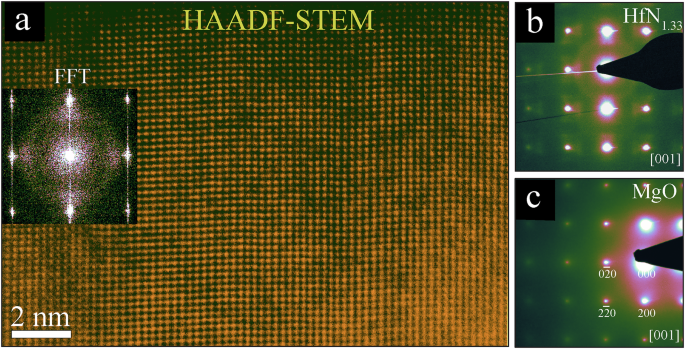
a Color-coded cross-sectional high resolution HAADF STEM micrograph of the HfN1.33 film recorded along the [001] zone axis and a small camera length for enhanced z-contrast. Nanometer-sized domains are seen as bright and dark areas. An FFT-inset show lobes of weak intensity from the sharp main spots. b, c Corresponding color-coded SAED patterns from the HfN1.33 film, with satellites around each main spot, and MgO substrate, respectively. The presence of any imaging artifacts in the diffraction pattern is ruled-out upon comparing with the adjacent substrate diffraction pattern and FFT. The diffuse circular ring in (b), centered around the direct beam, is attributed to the damaged amorphous surface layer from ion milling.
Accordingly, the identified 3D checkerboard superstructure explains the broad peaks labeled “S” in XRD in Fig. 1, as superstructure satellites. An increased nitrogen content results in more intense satellite peaks in XRD, while the peak position is maintained. The satellite position is related to the average superstructure period, <Λ>, of the checkerboard pattern, calculated using Eq. (1)27, where n is the satellite reflection order, θ0 is the angle of the main peak, and θn is the angle of the nth satellite peak27. Thus, an equal average period for both compositions. The 002 and 004 satellite separations of ∆2θ ≈ 11.9° and ∆2θ ≈ 15.5°, respectively, both yielded an average period of about <Λ> = 7.5 Å, where for a non-perfect ordering of nm-sized domains, only n = 1 can be expected.
This small period agrees well with the directly measured period in the STEM micrographs in Fig. 2. Additionally, the checkerboard pattern is aligned in the <001> directions, determined from the shape of the satellite lobes in electron diffraction and the fact that the domains are visible in STEM despite the projection of multiple domains in the comparatively thick foil. We submit that the Hf-rich domains are near-stoichiometric HfN, while the N-enriched domains, on the other hand, are hyper-overstoichiometric with accumulated Hf vacancies and interstitial N defects, as a means to reduce the system’s enthalpy. Thus, the checkerboard pattern is effective in minimizing the forced additional energy condition by virtue of mutual annihilation of inhomogeneous strain fields.
Density functional theory (DFT) calculations, ab-initio molecular dynamics (AIMD) and Monte Carlo (MC) simulations based on the machine-learning-interatomic potential (MLIP) trained during AIMD (see Supplementary Section 5) are employed to understand energetic mechanisms leading to defect superstructuring in HfN1.22 thin films. The propensity of HfN at incorporating cation vacancies and N interstitials is assessed by comparison with defect formation energies separately evaluated by DFT for TiN, due to the strong preference of TiN towards N-depletion28. Results in Table 1 indicate that cation vacancies (Vme) and N self-interstitials (NSI) are more stable in HfxN compared to TixN. In both nitrides, metal vacancies repel each other, consistent with previous results29,30, However, introducing nitrogen antisite (NAS) defects together with metal vacancies reveals different behavior of HfxNy versus TixNy. A single antisite defect in HfxNy has nearly 3 eV lower formation energy (8.72 vs 11.67 eV) compared to TixNy, which is a first indication that HfN can accommodate overstoichiometry by combining excess N with metal depletion. A further addition of metal vacancies near NAS defects results in a substantial reduction of the total defect formation energy in HfxNy. These results indicate that clustering of metal vacancies and nitrogen interstitials is less unfavorable in HfN.
The relatively high point defect formation energy calculated for both material systems suggests that a substantial concentration of N interstitials and cation vacancies can only be achieved in synthesis conditions far from thermodynamic equilibrium. The reactive magnetron sputtering conditions used in this work, with a growth temperature of 800 °C, satisfies this condition, with a homologous temperature of Tgrowth / Tmelt = 0.3 (Tmelt = 3300 °C). In addition, the continuous high flux of low energy ion bombardment introduces kinetic effects, where metal vacancies can form, and subsequently buried, through energetic collision cascades at and just below the surface of the growing film. Similarly, bombarding nitrogen ions may be trapped in interstitial positions or even in vacant cation sites.
The defect structure of HfN1.22 predicted by annealing/cooling cycles in AIMD (Fig. 3a) shows a striking resemblance with experimental results from STEM, SAED and XRD, confirming the hypothesis of quasi-stoichiometric and hyper-overstoichiometric domains in a checkerboard superstructure aligned in the <001> directions. The calculations yield a cubic lattice parameter of 4.56 ± 0.03 Å which, combined with the N/Hf composition (119/98 = 1.214), corresponds to a mass density of 12.4 ± 0.1 g·cm–3, in very good agreement with experimental results. The size of the domains is slightly overestimated in the calculations, with a checkerboard period of approximately 13.5 Å, while experiments show a period of 7.5 Å. The discrepancy may be due to the constraint imposed by the periodic boundary conditions of supercell calculations and by partial incommensurability of the supercell size with experimentally determined period.
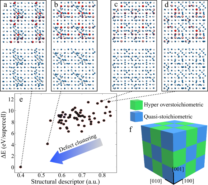
a–d Selected defect structures in Hf0.91N1.10 supercells with stochastic defect arrangements, mimicking HfN1.22 composition. e MLIP energies of a wide range of structures including the ones in (a–d). All supercells contain the same number of Hf98 and N (119) atoms on a 3 × 3 × 3 B1 lattice, and the snapshot is taken in the [001] zone axis. Note that the snapshots display four Hf0.91N1.10 supercell replicas. The two lowest-energy structures (a) and (b) are characterized by local agglomerations of cation vacancies (red spheres in upper part of supercell snapshots) decorated by N self-interstitials (blue spheres). Conversely, high-energy structures in (c) and (d) show a rather homogeneous distribution of defects over the entire supercell volume. A good reliability of the MLIP results was confirmed by re-relaxing the structures in (a–d) by DFT calculations (see Supplementary Section 5). f) Schematic of the 3-dimensional checkerboard superstructure with main <100> axes relating to the B1 NaCl lattice.
We use MLIP-MC sampling for rapidly screening the energy of different defect arrangements in HfN1.22. The differences in energy (∆E) from the most stable configuration correlate with a structural descriptor (Fig. 3e). The latter considers the spatial width of Vme distributions together with Vme/NSI distances. Thus, the structural descriptor serves verifying whether defect-clustering in HfN1.22 arises from energetic effects. As shown by Fig. 3a–d (with corresponding ∆E), defect clustering is unequivocally favored over a disordered random defect distribution. Combined with information from Table 1, we infer that cation vacancies tend to cluster only because of the simultaneous presence of N self-interstitials. The checkerboard superstructure, illustrated in Fig. 3f, has a great influence on the mechanical properties of HfN1.22, as discussed below, where the organized defects aid dislocation-mediated plasticity. It is worth noting that some defect configurations resemble those identified by DFT for metal-deficient TiC31, suggesting that defect structures similar to HfxNy could be realized in other carbonitrides.
Color-coded HAADF STEM micrographs in Fig. 4a–c reveal a dense dislocation structure in the as-grown HfN1.22 film. These threading dislocations form early in the growth process due to imperfections on the substrate surface as well as the large lattice mismatch and extend over the full thickness of the film. The threading dislocation density is ~1010 cm-2, approximated from the STEM images. However, the majority of the 7.5% lattice mismatch between MgO and HfN is relieved by misfit dislocations at the film-substrate interface.
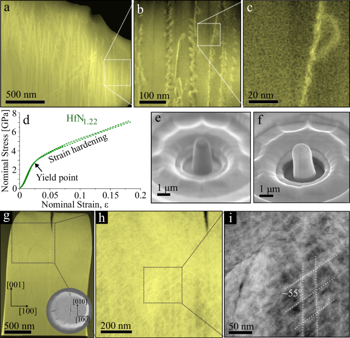
a–c Color-coded cross-sectional high-resolution HAADF STEM images in the [001] zone axis, highlighting dislocations. c Threading dislocation with a dislocation loop extension, in which the speckled contrast corresponds to the compositionally modulated superstructure. d Three stress-strain curves from milled micropillars during compression testing. e, f Representative SEM micrographs of as-milled and post-mortem pillars, respectively. In-depth post-mortem analysis was done using a lamella taken from the pillar in (f) by focused ion beam lift-out. g–i HAADF STEM micrographs in the [010] zone-axis. The overview micrograph in (g) shows that substantial mass-transport has taken place in the top half of the pillar. The inset is a top-view SEM micrograph with markings of the crystal directions. The high dislocation density in (h) and marked dislocations in (i) show an average dislocation tilt of approximately 55° with respect to the sample normal. A ~ 400 nm long surface crack and a ~ 200 nm long crack in the bulk of the pillar were effectively stopped without catastrophic fracture. Supplementary Fig. S9 in Supplementary Section 6 show arcs in SAED patterns of the pillar in g) which give further evidence of ductility.
Most threading dislocations are, in addition, associated with multiple tightly spaced dislocation loops that fan out by 10–20 nm, attached to a vertical threading dislocation, suggesting that the threading dislocation lower the nucleation barrier for dislocation loop formation. The checkerboard point defect structure in the present HfNy films (speckled contrast in Fig. 4c) is disturbed in the presence of the threading dislocations which therefore may cause point defects diffusion and accumulation, ultimately condensing into a dislocation loop nucleus. Thus, we believe that the cause of the dislocation loops is due to a rearrangement of the Hf-vacancies in close proximity to the threading dislocation. An accumulation of vacancies increases the local strain which may cause additional Hf-vacancy diffusion, resulting in a loop expansion. The local strain will, however, decrease with an increasing loop radius as the lattice distortion is spread over a larger area. Thus, a relatively uniform dislocation loop size is obtained as the driving force for expansion is reduced below the critical point required for vacancy diffusion. The N-interstitial point defects are not expected to generate dislocations loops as the relatively small N atom can be more easily accommodated in the lattice.
Similarly, isolated dislocation loops has been found in ion-assisted magnetron sputtered TiN single crystal thin films, where the density of dislocation loops increased with the number of point defects created during growth, in turn affected by both growth temperature and ion energy22. The apparently substantially reduced nucleation barrier for new dislocations in the present HfNy film as caused by the high point defect density, in particular Hf-vacancies, is encouraging for an improved plasticity of the material, more akin to the behavior of ductile metals than brittle ceramics.
The HfN1.22 and for HfN1.33 films both qualify for hard coatings with a nanoindentation hardness of 26.0 ± 2.3 GPa and 27.7 ± 0.9 GPa, respectively, similar to reports for HfNy25,32, and HfAlN33 films. Seo et al. also observed a substantial increase in hardness upon deviation from stoichiometric HfNy films, where H = 32 GPa was found for HfN1.3218. They attributed the hardness increase to dislocation pinning at Hf-vacancies and N-interstitials, increasing the resistance to dislocation glide. With a similar argument, we instead attribute the increase of hardness to the checkerboard superstructure, with ordering of point defects along <001>, where the more pronounced checkerboard pattern in HfN1.33, are more effective at pinning.
Figure 4d shows the stress-strain curves of uniaxially compressed micropillars milled from the HfN1.22 film. All three compressed pillars deform consistently with a small scatter in the stress-strain curves and a notably high level of ductility. The yield point occurred at a nominal stress of ~2.6 GPa at a plastic strain of ~2%, followed by ductile deformation and significant strain hardening of the material. None of the pillars failed catastrophically and the loading was stopped after a nominal strain of 7% and 15%. The maximum recorded stress was more than 7 GPa due to strain hardening, nearly triple the yield strength, while the ultimate strength was not reached. Representative scanning electron microscopy (SEM) micrographs of the pillars pre- and post-mortem, and a post-mortem HAADF STEM overview in Fig. 4e–g show that the top-half of the pillar underwent ductile plastic deformation. The behavior of such global plasticity is rare for hard transition metal nitrides but resembles ductile metals with large dislocation mediated mass transport. Typically, complete brittle fracture or localized massive slip just past the elastic region appears in micropillar compression tests of close-to-stoichiometric transition-metal nitride and carbide hard coatings34,35,36,37,38,39.
The pillar plastic deformation and strain hardening are further examined through high-resolution HAADF STEM imaging in Fig. 4g–i. The brighter contrast in the top half of the pillar stems from an increased dislocation density compared to the as-grown film. A dense dislocation network has evolved (Fig. 4h), which makes for a ductile work hardening mechanism associated with metals, where the dislocation network inhibits further dislocation movement and multiplication40. On average, two distinct directions of the dislocations can be observed: as-grown vertical threading dislocations in [001], and others with a ~ 55° angle to the vertical. The vertical dislocations appear sessile as the number density correspond rather well with the intrinsic threading dislocation density. However, no sign of the intrinsic dislocation loops can be found in the compressed pillar, indicating that these loops have moved and expanded through the lattice, which can partly explain the remarkable plasticity. The substantially increased dislocation density also suggests nucleation of additional dislocations. Given the tilt angle of ~55° with respect to [001] and previous report of preferred slip system in HfN41, we assign these nucleated dislocations to the {111} < 110> slip system. The enhanced ductility can thus be explained by motion of dislocation loops and a low barrier for dislocation nucleation. Both of which are attributed to the large number of point defects in the lattice, in particular Hf-vacancies, as discussed above.
An additional series of 28 pillars with diameters of 810 nm, 640 nm, 480 nm, and 300 nm were milled from the HfN1.22 film to assess potential size effects of the plastic response. Moreover, the plastic response of HfN1.33 was evaluated using 7 pillars of 300 nm diameter. The resulting engineering stress-strain curves are presented in Fig. 5a, b. Despite up to 50% strain, not a single pillar failed catastrophically, showing an extraordinary malleability. SEM micrographs of compressed HfN1.22 pillars (810 nm) are shown in Fig. 5c–f, representative for all of the compression tests except for 300 nm diameter HfN1.22 pillars, see Fig. 5g, which tend to deform differently. A remarkable agreement in the stress-strain curves was obtained for the three larger sized HfN1.22 pillars. A larger disagreement was found for the smallest diameter, 300 nm, where the yield stress substantially increased and the flow stress, i.e. strain hardening rate, SHR, substantially decreased, indicating an onset of significant size-effects. Although calculating SHR from engineering stress-strain curves is not recommended, it gives a reasonable indication of the true value and enables a comparison between the samples in this study. The yield stress and strain hardening rates are plotted in the inset of Fig. 5a, which clearly shows the deviation, and is attributed to a change of the deformation mechanism. The 300 nm diameter HfN1.22 pillars, in addition to the uniform plastic deformation with material being symmetrically squeezed out, also exhibited pronounced shearing at 39.5% strain, and even some fracture or slip at >50% strain. This change may be related to the mechanical annealing effect which becomes stronger at smaller pillar sizes42. For larger pillars, the yield stress increased slightly with decreasing size.
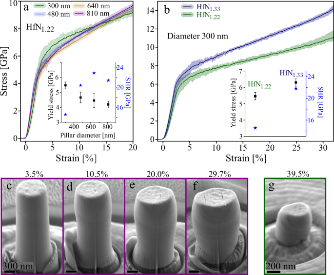
a Average engineering stress-strain curves for compression of HfN1.22 pillars with different sizes to evaluate size effects. b Average engineering stress-strain curves for compression of 300 diameter pillars of HfN1.22 and HfN1.33, respectively. The insets in (a, b) show the yield stress and the strain hardening rate, SHR. The error (max, min) is given by the colored areas around the average line. c–f SEM micrographs of 810 nm diameter HfN1.22 pillars compressed to different amounts of strain, up to ~30%. g SEM micrograph of a 300 nm diameter HfN1.22 pillar compressed to ~40% strain, exhibiting a different plastic deformation. More details on stress-strain curves and SEM micrographs are presented in Supplementary Section 6.
The pillar taper and diameter selection can significantly affect the calculated stress-strain curves and the yield and flow stresses43. As seen in Fig. 5c–f, the plastic deformation starts at the top of the pillar and progressively grows downwards at increasing strains. For accurate yield stress measurement, the top diameter is used for stress-strain calculations from the load-displacement data. However, a consequence of the non-zero taper is an increased flow stress during plastic deformation, due to the gradually increasing cross-sectional area of the plastically deformed zone. This effect, estimated by analyzing the plastically deformed zone at different strains from the SEM micrographs (see Fig. 5 and Supplementary Section 6, Supplementary Figs. S10–S14) and considering the ~2° taper, contributes up to 6.6 GPa of the SHR for 810 nm pillars. Thus, up to 30% of the SHR is caused by the taper, while more than ~70% is attributed to real strain hardening effects from interacting dislocations, as discussed above. The mechanical response from Fig. 4d agrees qualitatively very well with the results in Fig. 5a: No catastrophic failure and substantial strain hardening. However, differences in test parameters—like the ~4.5° taper and mid-point diameter – fully explains the lower yield stress and larger SHR in Fig. 4d. Therefore, the results in Fig. 5 are considered more accurate.
The comparison of the stress-strain curves between 300 nm pillars of HfN1.22 and HfN1.33 in Fig. 5b, shows that HfN1.33’s higher overstoichiometry improves the mechanical performance. A substantially increased yield stress (6.3 ± 0.23 GPa), compared to HfN1.22 (5.5 ± 0.23 GPa) was obtained, and a similar SHR to the larger HfN1.22 pillars. Together with uniform plastic deformation of the HfN1.33 pillars, (see Supplementary Section 6, Supplementary Fig. S14) suggests minimal size effects for HfN1.33. The higher yield strength of HfN1.33 correlates well with its higher hardness, attributed to more effective dislocation pinning by the more pronounced checkerboard superstructure. Thus, a larger overstoichiometry from an increased number of Hf-vacancies and N-interstitials results in a stronger material that simultaneously allows for effective dislocation generation, even at very small dimensions.
B1 NaCl-structured transition metal nitrides and carbides have dislocation Burgers vector along the close-packed <110> directions and glide-planes on {111}, {110} or {001}. Recent experiments evidenced the presence of {001}<110>, {110}<110>, and {111}<110> edge dislocations in as-deposited epitaxial TiN films44. Nevertheless, different dislocations may present substantial differences in core energy and Peierls stress, where both are affected by the local stoichiometry. The primarily activated plane is determined by the orientation of the load in relation to the crystal axes and by the energy required for dislocation nucleation and/or motion on respective plane. Many hard coating materials prefer to slip on the {110} planes at room temperature38,39,45,46,47,48,49,50, For TiN, nearly twice the critical stress is required to nucleate a dislocation on {111} compared to {110} planes49.
The Schmid factors in the present experiment with compression in [001] and slip in <110> directions are calculated for different planes: 0 for {001}, 0.5 for {110}, and 0.408 for {111}. The critical resolved stress is thus highest in the {110}<110> slip system, however as noted above, different material systems can prefer certain slip systems over others, where HfN1.22 instead prefer the {111}<110> slip system. This may enable an enhanced ductility because of twice as many slip systems compared to {110}<110> and considering the geometry of the compression experiment. However, the exceptional room-temperature ductility of HfN1.22 and HfN1.33 cannot be explained solely by a different preferred slip system. Instead, the large threading dislocation density of 1014 m-2, and particularly the even more abundant dislocation loops (Fig. 4b) play an active role in the plastic response by dislocation motion. Furthermore, the nucleation of new dislocations can continue by rearrangement of remaining vacancies due to the externally applied strain in the same way discussed previously, thus enabling an enhanced ductility. Similar metal-like behavior of room temperature brittle oxide ceramics has been reported in several cases after introducing a sufficiently high dislocation density4,5,6, It should, however, be noted that plasticity in brittle ceramics is common at elevated temperatures51,52, including HfN at 2300 °C41.
The SEM micrographs in Fig. 5e–f and the STEM analysis of the post-mortem HfN1.22 pillar in Fig. 4g–i reveal an improved fracture toughness by the effectively stopped vertical surface crack after ~400 nm, that initiated on the (010) plane, where {001} are common cleavage planes in transition metal nitrides due to their lowest surface energy53. Furthermore, a small crack within the pillar, Fig. 4i, ~200 nm long, was also stopped in its path. The toughening mechanism could be crack tip blunting due to dislocation emission near the tip54, enabled by the apparent low dislocation nucleation barrier.
Conclusions
Single-crystal HfN1.22 and HfN1.33 films with a compositionally modulated superstructure were grown by ion-assisted reactive magnetron sputter epitaxy on MgO(001) substrates. The superstructure exhibits checkerboard structure along <001> directions, with a period of about 7.5 Å. It forms during film synthesis by excess N segregating to hyper-overstoichiometric domains with agglomerated Hf-vacancies and N interstitials, together with domains of quasi-stoichiometric HfN. The experimental results are supported by ab-initio calculations showing a high propensity of HfNy to form cation vacancies and interstitial nitrogen and support the agglomeration of existing defects. Micropillar compression tests of sculptured HfN1.22 pillars reveal metal-like global plastic deformation with activation of multiple {111}<110> slip-systems and large strain hardening due to dislocation interactions. Concurrently the films exhibit a high hardness. The noteworthy room-temperature ductility is facilitated by a high intrinsic dislocation density from growth, including mobile dislocation loops and facile dislocation nucleation enabled by the checkerboard superstructure. An improved toughness is shown by effective crack-arrest. Such durable hard coating properties present a long sought-for improvement for applications in tough environments, and we believe that this innovative nanoscale superstructuring can be applied to various nitride and carbide ceramics for coating applications.
Methods
Growth and Composition
The films were grown by reactive DC magnetron sputtering in a high-vacuum chamber having background pressure lower than 6.4 ×10⁻⁴ Pa. A d = 75 mm (3”) elemental Hf-target (99%) in coupled unbalanced type II magnetron configuration was used to sputter in Ar + N2 gas mixture at 0.6 Pa with a N2 partial pressure of 0.067 Pa at 800 °C. The MgO(001) substrates were cleaned and pre-annealed (900 °C for 1 h) before deposition using the procedure outlined in55: sonication in detergent (2 vol%), de-ionized water, acetone and ethanol respectively.
High flux of low energy ion assistance was applied to the growing film using a −30 V substrate bias for improved magnetron sputter epitaxy. The target plasma was extended and directed to the substrate table using a solenoid around the substrate table, which coupled the magnetic field from the magnetron as explained elsewhere56. The ion-to-metal flux ratio, incident on the sample and the ion energy was calculated from results obtained by area (1 cm2) and Langmuir (W-wire, d = 0.5 mm) plasma probes57. Deposition parameters and results of the two films are listed in Table 2. Both ion energy and ion-to-atom flux ratio can affect the film growth substantially21,22,23, in particular for denser films and a layer-by-layer growth with a particular texture.
The chemical composition of the films was analyzed by a combination of Rutherford backscattering spectrometry (RBS) and time-of-flight elastic recoil detection analysis (ToF-ERDA), where the latter was used to quantify lighter elements. Both experiments were conducted at the tandem accelerator at Ångströmslaboratoriet, Uppsala University. As RBS and ToF-ERDA analysis require thin samples, ~200 nm thick films were deposited on Si(001) substrates at otherwise identical conditions. For RBS a 2 MeV 4He2+ probe was incident at 5° to the sample normal and detector at a 170° scattering angle while the sample was continuously tilted in small random motions about 2° around the setpoint. Reference samples (Au, Cu, SiC, TiN) was used for analysis using SimNRA58. ToF-ERDA used a 36 MeV 127I8+ probe incident at 22.5° to the sample surface and with a scattering angle of 45° to the detector. The ToF-energy histograms were analyzed using Potku software59. In combination, the composition error is estimated to be better than 0.03 for the metal/nitrogen ratio. The RBS simulation also provided surface density of the film which was used to calculate:
-
1.
The mass density of the films by comparing with the film thickness.
-
2.
The ion-to-metal flux ratio by combining the results of the plasma area probe and calculating the number of Hf atoms arriving on the substrate per second.
Structural characterization
X-ray diffraction (XRD) θ-2θ scans were acquired using a Panalytical X’Pert Pro powder diffractometer with monochromatic Cu-kα radiation in the Bragg-Brentano geometry. A divergence and acceptance slit of ½° were used. ω-scan rocking curves were acquired in a Panalytical Empyrian with high-resolution optics, hybrid Cu-Kα monochromator and 3-bounce Ge-crystal analyzer. Reciprocal space maps were used to evaluate the film quality, relaxed lattice parameter, a0, limited lateral size, L, (lateral x-ray coherence length) and mosaic tilt. More details on calculations and analysis can be found in Supplementary Section 3. The maps were acquired in the same diffractometer using a hybrid monochromator, and an open 2D pixel detector was operated in scanning line mode for faster acquisition.
Cross-sectional transmission electron microscopy (TEM) samples of the as-grown films were prepared by a standard method where two cut pieces of the sample are sandwiched and glued face-to-face in a Ti-grid, mechanically polished until ~50 μm thickness and ion-milled until electron transparent using 5 keV Ar+ at a 5° incidence angle, followed by 25 minutes of ion polishing at 1–1.9 keV. Atomic resolution high angle annular dark field scanning transmission electron microscopy (HAADF STEM) was performed in Linköping’s double Cs corrected Titan3 60-300 microscope, operated at 300 keV. Selected area electron diffraction (SAED) patterns were acquired in a FEI Tecnai G2 microscope operated at 200 keV.
Computational details
Kohn-Sham density-functional theory (DFT) calculations and ab initio molecular dynamics (AIMD) simulations were carried out using VASP60, implemented with the projector augmented wave method61 and the Perdew-Burke-Ernzerhof (PBE) approximation62 to the electronic exchange and correlation energies. Among various local and semi-local functionals, the PBE approximation has been shown to be the most accurate at reproducing experimental values of monovacancy formation energies in elemental metals63.
DFT calculations evaluate the formation energies of isolated point defects, small defect clusters, as well as the energies of defect distributions with stochastic and ordered arrangements. Metal vacancies, VMe, nitrogen in antisite (cation) position, NAS, and nitrogen self-interstitials, NSI, were introduced into supercells comprised of 108 anion and 108 cation sites, corresponding to 3x3x3 conventional NaCl-structure unit cells. In AIMD, the composition of HfN1.22 was mimicked by Hf0.91N1.10, in a supercell with 98 Hf and 119 N atoms.
DFT calculations of defect formation energies in nitrides require reference chemical potentials for nitrogen and metal species. We adopt N2 gas molecules and hcp metals as done in previous DFT studies29,30, To compute the energies of hcp metals, we employ 8-atom supercells with 12 × 12 × 12 Monkhorst-Pack (MP)64 k-point meshes and 500 eV cutoff energies. The N2 dimer is placed in a cell with size of 15 × 15 × 15 Å3. The molecule’s energy and the N ≡ N equilibrium distance are computed using a planewave cutoff of 700 eV.
To obtain DFT and AIMD predictions with equal level of accuracy, we perform all computations and simulations using 2 × 2 × 2 MP sampling of the reciprocal space and 400 eV cutoff energies for the planewave basis set. These parameters yield a good balance between computational efficiency and accuracy. In DFT calculations, conjugate-gradient optimization of all structural degrees of freedom is reiterated to meet an energy accuracy of 10–5 eV/supercell and a force accuracy of 10–2 eV ∙ Å-1. In AIMD, forces on atoms are computed when the electron-density iterations reach an accuracy of 10–5 eV/supercell. The equations of motion are integrated on a time-step of 1 fs.
The identification of representative defect arrangements in HfyNx is done with the aid of AIMD. AIMD simulations are assisted by on-the-fly training of a machine-learning interatomic potential (MLIP), as implemented in VASP 6.4.3. The flowchart in Supplementary Section 5 provides a schematic description of the procedure. Briefly: we construct HfN1.22 supercells with lattice structure, chemical composition, and density that mimic the information collected by experimental characterization. AIMD simulations employ velocity-rescaling to control a cyclic annealing/cooling scheme between 300 and ≈2500 K. Annealing promotes diffusion and reorganization of point defects. The simulations follow the structural evolution during 0.2 ns. The structure obtained from the final cooling is fully relaxed by DFT at 0 K. As explained in the results and discussion section, our procedure leverages a representative defect configuration and outputs an MLIP able to describe accurately different Hf-N environments.
The energies of the defect structures in the supercell are computed by conjugate gradient relaxation using MLIP. Figure 3e shows that the energy of the configurations sampled via MC correlates well with a structural descriptor (D). The descriptor is defined as: D = std · λ, where std is the standard deviation of the spatial distribution of cation vacancies, while λ is the sum of the distances of N self-interstitial defects from the average Cartesian coordinates of the vacancy cluster. Hence, the correlation shown in Fig. 3e indicates two structural conditions that tend to lower the defect energy in Hf0.90N1.10 (≡ HfN1.22) supercells: (i) cation vacancies prefer to spread out over a relatively narrow volume and – at the same time – (ii) the N self-interstitial defects favor positions closer to the vacancy cluster.
Mechanical characterization
Nanoindentation using a Hysitron TI950 was used to measure film hardness. It was equipped with a Berkovich diamond tip with a radius of ~30 nm. Analysis was done according to the method by Oliver and Pharr65. 25 indents were measured for both samples at a load of 5 mN, resulting in an indentation depth of <90 nm, satisfying the 10% rule-of-thumb.
Cylindrical micropillars with a diameter of approximately 1 μm were milled on the HfN1.22 film surface by focused ion beam (JEOL JEM-9320) system operated at 30 kV. An aspect ratio of ~2-3 was used (height/diameter). Compression tests were carried out in a load-controlled nanoindenter SHIMADZU DUH-211S equipped with a 20 μm flat-punch diamond tip at ambient temperature. An initial strain rate of all micropillars was controlled to approximately 10−2 s-1. The pillars had a taper of ~4.5°, and the diameter for calculating the stress was taken as the average of the top and bottom diameters. The deformed micropillars were observed using a field-emission scanning electron microscope, JEOL JSM-7001FA. An electron transparent lamella of a representative compressed micropillar was prepared by conventional lift-out method using Carl Zeiss Crossbeam 1540 EsB focused ion beam/scanning electron microscopy workstation. Before thinning and lift out, an electron beam-induced Pt layer was deposited to provide protection from gallium implantation. For final thinning, a low-energy milling at 2 kV was performed to minimize Ga-induced damage.
An additional set of micropillars were tested from both HfN1.22 and HfN1.33 to verify the results presented in Fig. 4 and compare the two material compositions. Various HfN1.22 pillar diameters were tested to evaluate the size effect: 810 nm, 640 nm, 480 nm and 300 nm. They were milled by a focused ion beam using a ThermoFisher Scios 2. The geometries were prepared using a Ga-ion probe current of 5 nA for the rough cut down to 50 pA for the finishing step. In-situ pillar compression was done in a Zeiss Sigma 500 VP system using FemtoTools FT-NMT04 in-situ SEM nanoindenter equipped with a 7 µm diameter flat diamond punch in a displacement-controlled mode with a displacement rate of 10 nm∙s-1. The pillars were loaded to different strains, up to a maximum of ~50% strain.
The correct alignment between the sample and tip was guaranteed by the following procedure: Before the actual loading of the pillar, indentation tests were carried out in the pristine coating, making sure that there was a sharp transition between the force recording in the vacuum and the loading of the film. Given that the angle between the two parts cannot be modified with this instrument, and the specimen must always be positioned the same way on the specimen holder due to the instrument’s design, a one-time FIB alignment procedure was performed on the flat punch tip. The compressed pillars were imaged at a ~ 50° tilt angle by a Zeiss Sigma 300 scanning electron microscope using a 3 kV acceleration voltage and SE2 detector.
The load-displacement curves were converted into engineering stress-strain curves following an approach by Wheeler and Michler66, where the top diameter of the pillar is taken as the reference contact area. The engineering strain was obtained from the displacement data using the pillar height and a corrected displacement data accounting for the base compliance following Sneddon’s correction67 given by:
where νSub and ESub are the biaxial Poisson’s ratio and Young’s modulus of the substrate, respectively, νsub = 0.18, Esub = 291 GPa68. F is the applied force, and d is the diameter of the pillars. ΔL is then the deformation of the substrate induced by the pillar and must be subtracted before calculating the strain.
The engineering stress-strain curves were further analyzed by binning the data in steps of 0.05 % strain. An average of the stress was calculated, a minimum of 3 pillars for each diameter was compressed to >30% strain except the pillars with 480 nm diameter, where a minimum of 3 tests was conducted up to ~23% strain. The minimum and maximum values of each set of pillars were taken as error bar. The strain hardening rate was calculated from the linear part of the flow stress from the average curves. The expected strain hardening rate was calculated by assuming a 2° taper and estimating the deformation region from SEM micrographs.


Responses