Modulation of the electromagnetic shielding effectiveness through micro/macrostructure design for electronic packaging
Introduction
Electronic packaging materials dissipate heat and provide physical and environmental protection to electrical components. For IC chips, the packaging material should possess excellent thermal conductivity, high EMI SE, high mechanical properties, moisture resistance, and long-term stability1,2. For antennas or antenna arrays, the packaging material should also possess the same properties, except that the EMI SE should be low to efficiently radiate electromagnetic (EM) waves3. Therefore, to alleviate the costs of multiple packaging materials and processes for each component in an electronic device, methods to tailor the EMI SE of one material are needed4,5. The codesign of electrical, mechanical, and thermal properties is particularly crucial for ensuring high performance and high reliability in high-power density systems for applications in robotics, autonomous vehicles, etc.6,7,8. Although metals have high EMI SE, they are heavy and susceptible to corrosion, and it is difficult to tailor their properties. Polymer composites containing functional nano or micro fillers are therefore preferred. Although tailoring the mechanical and thermal properties of polymer nanocomposites by controlling their microstructure is well established9,10,11, the micro/macrostructure-EMI SE relationships are much less explored.
High EMI SE can be obtained in polymer composites by increasing their electrical conductivity, for example, by incorporating anisotropic electrically conductive nanofillers such as graphene, carbon nanotubes, or MXene2,12,13. Then, controlling the orientation of the fillers enables tailoring of the composite’s properties14,15,16,17. For EMI SE, aligning conductive fillers enhances the electrical conductivity along the alignment direction, leading to high impedance mismatch and EM wave reflection18. Processes such as freeze casting, tape casting, or self-assembly can be employed to obtain composites with aligned microstructures and high EMI SE along one direction19. For instance, freeze-cast MXene/cellulose nanofibril aerogels with anisotropic channels cut at various angles exhibit a tunable EMI SE that varies with the orientation of the channels. When the angle is increased from 0°, parallel to the external electric field direction of the incident EM waves, to 90°, the total shielding effectiveness (SET) decreases from 63 dB to 36.5 dB20. However, all the MXenes that are present in the scaffold do not have their orientation tailored precisely in any arbitrary direction due to the limitations of the freezing method. In another example, NiCo2O4-coated GO/carbon fibers aligned in silicone at specific angles cut from unidirectionally aligned samples also exhibit similar variations: the samples with fibers perpendicular to the direction of propagation of the EM waves have the highest EM absorption (SEA)21. Unfortunately, cutting aligned samples at different angles is not an efficient process for practical applications. Another promising approach for controlling material properties is 3D printing22,23. Indeed, 3D printing can create architected composites with honeycomb, hollow, or lattice structures that are low density and that effectively attenuate EM waves through multiple reflections and scattering22,24. For instance, 3D-printed honeycomb architectures made of graphene-carbon nanotube-polylactic acid composites, with a pore size less than the incident wavelength/5 (<λ/5) corresponding to 7.2–4.8 mm, promote more multireflection and scattering events on the wall of the pore units and exhibit higher absorption SEA and EMI SE values of 35–45 dB24. In another example, the 3D-printed infill pattern is tuned: printed samples with cross-ply and angle-ply patterns show higher EMI SE than unidirectional ply patterns25. However, there is no example in which the local filler orientation is combined with the macroscopic shape using 3D printing to tailor the EMI SE in composites in 3D.
To study the synergetic effects of micro- and macrostructures on EMI SE, recent advancements in 3D printing using external fields such as shear, acoustic, magnetic, and electrical fields can be employed26,27. For instance, direct ink writing (DIW) extrusion-based 3D printing, where the ink is dispensed out of small nozzles under controlled flow rates and deposited along digitally defined paths to fabricate 3D structures layer by layer, can align conductive microfibers along the printing direction to enhance the electrical conductivity. However, this approach does not permit local tailoring of the 2D microplatelet orientation in any desired direction28. Interestingly, one unique method that allows this capability is magnetic direct ink writing (M-DIW)27. M-DIW continuously prints liquid inks containing water in which magnetically responsive 2D microplatelets are suspended. As the ink is deposited onto a porous substrate that removes the water and consolidates the layer, a rotating magnetic field with a strength of approximately 50 mT orients the microplatelets. As the nozzle moves on the porous print bed, the orientation of the rotating magnetic field can be changed to orient the microplatelets locally at any desired angle. Meanwhile, the printing path can create the desired patterns and shapes. Using an ink containing electrically conductive 2D microplatelets, such as graphite, enables the fabrication of composites with high electrical conductivity. Therefore, M-DIW is an ideal process for investigating how micro/macrostructure designs can tailor the EMI SE and the other properties required for making high-performance and reliable electronic packaging.
In this study, we explore the effects of micro/macrostructure design on the EMI SE of high-density graphite-based materials prepared using M-DIW. The aim of this study is not only to optimize the performance of the material in terms of EMI SE but also to demonstrate an easily applicable method for tailoring the performance using micro/macrostructure design. First, three proposed designs are described and explained: unidirectional microstructure, asymmetric microstructure, and asymmetric micro/macrostructure. Scaffolds containing these structures are then produced experimentally using M-DIW and a postprinting thermal treatment, with the angle θ of the unidirectional microstructure varying from 0 to 90°. The electrical conductivity, porosity, microstructure, morphology, and EMI SE of the scaffolds were characterized. The asymmetric microstructure, which is a bilayer with (theta)=0° and 90° orientations, is tested for EM waves coming from each side. Subsequently, macroscopic pillar arrays with local microstructures are 3D printed to demonstrate the synergistic effect of micro- and macrostructures on the EMI SE. The thermal and mechanical properties of the polymer-infiltrated scaffolds developed in this study were also characterized to demonstrate the possibility of codesigning multiple properties for customizable electronic packaging solutions.
Results
Micro/macrostructure conceptual design for EMI shielding
To tailor the EMI SE of a material containing percolating electrically conductive microplatelets, we propose combining microstructural and macroscopic designs (Fig. 1). Indeed, the electrical conductivity of the shielding material is critical to yield a large permittivity, leading to impedance mismatch and the reflection of normally incident EM waves29. Tailoring the microstructure and shape of materials will therefore impact their local electrical conductivity and EMI SE.
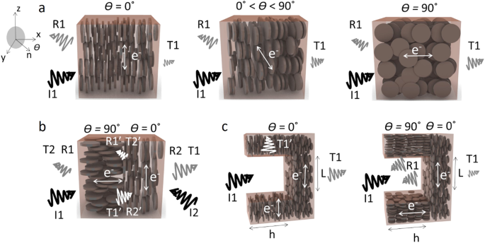
The incident direction of the EM wave is along the x-axis. θ is the orientation angle of the microplatelets defined by the angle between the normal to the microplatelet n and the incident direction of the EM wave. Shielding scenarios when an incident EM wave (I1, I2) is striking a material with (a) unidirectional microplatelet orientation at θ = 0˚, 0° < θ < 90°, and 90°, (b) asymmetric bilayer structure with θ = 0° and 90° and (c) micro/macrostructural design with 2 pillars and with θ = 0° throughout the structure (left) and θ = 0° in the base and 90° in the pillar (right). The direction of the highest electrical conductivity is indicated by the white arrows. R1, R1’, R2, and R2’ are the reflected EM waves, and T1, T1’, T2, and T2’ are the transmitted EM waves. h and L are the height of the pillars and the distance separating the 2 pillars, respectively.
The first microstructural design we propose to study involves unidirectionally aligned microplatelets oriented at various angles to tune the impedance mismatch between the air and the shielding material (Fig. 1a). Indeed, for such orthotropic materials, the dielectric constant is a tensor that varies with the angle θ between the normal to the biaxial alignment of the microplatelets and the incident direction of the EM wave, as follows30:
where ({varepsilon }_{perp }) is the dielectric constant perpendicular to the plane of the microplatelets, and ({varepsilon }_{parallel }) is the dielectric constant parallel to the plane of the microplatelets (see Supplementary Information (SI) Fig. S1 for details). Similarly, the permeability tensor can also be assumed to be a function of the angle θ:
where ({eta }_{perp }) and ({eta }_{parallel }) are the permeabilities perpendicular and parallel to the plane of the microplatelets, respectively. The intrinsic impedance Z of the material therefore also varies with the angle θ as follows:
(Z) is also related to the reflection coefficient ({S}_{11}) and the transmission coefficient ({S}_{21}) from the scattering matrix, as follows30,31:
Based on (1–4), we can reasonably assume that tuning the orientation of the electrically conductive microplatelets will tune the impedance Z and therefore change the impedance mismatch between the air and the shielding material, influencing the penetration and reflection of the incoming EM waves. Due to the large contact surface between the microplatelets and free electrons delocalized in the plane, the electrical conductivity of the materials built from microplatelets such as graphite along the plane is higher than that of the out-of-plane materials32. Therefore, the microstructure θ = 0° has a greater electrical conductivity in the plane (yz) perpendicular to the incoming EM wave direction (x) than in the other planes. Similarly, the microstructure θ = 90° has a higher electrical conductivity in the plane (xz), parallel to the incoming EM wave direction (x), than in the other planes. Since the delocalized electrons are scattering EM waves, it is therefore expected that the samples with the orientation θ = 0° will reflect more EM waves and have a greater EMI SE than the samples with the orientation θ = 90°. Therefore, tuning the orientation angle of the aligned microplatelets would be an effective way to tailor the EMI SE.
The second microstructural design we propose to study is an asymmetric bilayer in which two different microplatelet orientations are assembled within the thickness of the material. This change in the orientation of the microplatelet and thus in the direction of the electron conduction path is expected to create an additional interface with an impedance mismatch susceptible to further scattering of the EM waves. Indeed, based on (1–4), it can be expected that (Z(theta ={{0}^{circ}}),ne ,Z(theta ={{90}^{circ}} )). Furthermore, another advantage of building such an asymmetric microstructure is the possibility of creating a material that behaves differently depending on the direction of the incoming wave (Fig. 1b). If the EM wave enters the material from the left (I1 in Fig. 1b), it is more likely to penetrate the material with less reflection and to be scattered mostly at the interface between the two layers. If the EM wave enters the material from the right (I2 in Fig. 1b), a large portion of the wave will likely be first reflected due to the large impedance mismatch caused by the orientation θ = 0°, as discussed before, while a small portion will be additionally scattered at the junction between the two layers. It can be expected that the impedance mismatch when entering the composite will dominate the scattering of the EM wave in this structure when entering following I2. As a result, the material would have a lower EMI SE for waves incoming from the left (I1) than from the right (I2). Such a type of material could be very interesting for antennas that emit waves but should not receive signals from other components, for example.
Finally, to further enhance the EMI SE, we propose combining a microstructure with a macroscopic shape to generate multiple reflections and scattering events, eventually leading to increased EM wave attenuation (Fig. 1c). Indeed, previous works reported that surface features lead to multiple surface reflections24. Based on the previous hypothesis that electrically conductive microplatelets oriented perpendicularly to the incoming wave (θ = 0°) yield the most EM wave reflections, we propose adding surface pillars of height h separated by a distance L. In Fig. 1c, for convenience, the pillars are oriented horizontally, and the base on the right of the structure is vertical. In the structure, the microplatelets are either perpendicular to the contour of the pillar (θ = 0° throughout the structure, Fig. 1c, left) or following the contour of the pillar (θ = 90° in the pillar and θ = 0° in the base, Fig. 1c, right). When the microplatelets are aligned at θ = 0° throughout the structure, one can expect the EM waves that are scattered from the base (R1) to be able to penetrate the pillars if they are parallel to the microplatelets (T1’), whereas in the other case (θ = 90° in the pillar and θ = 0° in the base), the scattered waves R1 should also be reflected by the pillar. Overall, one can expect the design with the microplatelets following the contour of the pillar to exhibit the highest EMI SE.
Based on the above proposed micro/macrostructure designs, a 3D printing method that allows the control of the 3D shape of the microplatelet orientation is expected to eventually facilitate physical realization. Therefore, we herein used M-DIW and a previously established graphite-based ink. However, the fabrication process of graphite-based structures needs to be optimized to ensure high electrical conductivity and therefore high EMI SE. These structures will form a scaffold that will subsequently be infiltrated with a polymer to yield electrical packaging.
Fabrication of microstructured scaffolds with high EMI SE
To experimentally achieve the proposed designs, M-DIW and magnetically assisted slip casting (MASC) are employed. M-DIW is a more complex version of a process than MASC. In the following, simple microstructures could be easily obtained by employing MASC since there is no variation in the 3D shape. The ink made of magnetically responsive graphite microplatelets (mGr) follows an established recipe14,33, but the consolidation and electrical conductivity of the final dense microstructured scaffolds are optimized using heat treatment to achieve a high EMI SE (Fig. 2).
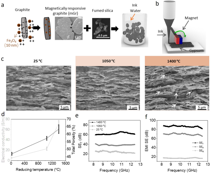
a Preparation of the aqueous mGr ink. b Schematic illustrating M-DIW. c Electron micrographs of cross-sections of scaffolds aligned at θ = 0° after heat treatment in a reducing atmosphere at 25, 1050 and 1400 °C. The white arrows indicate Fe3O4 aggregates. d Electrical conductivity, total porosity and (e) SET of the scaffolds (thickness = 0.75 mm, θ = 0°) after reduction at 25, 1050 and 1400 °C. f SET, SEA and SER of the scaffolds (thickness = 1.5 mm, θ = 0°) after reduction at 1400 °C.
Graphite microplatelets were chosen due to their high electrical conductivity, high quantity and affordability, and suitability for use in the MASC and M-DIW processes. To enable their orientation under an external magnetic field, the graphite microplatelets were first made of magnetically responsive graphite (mGr) by coating with superparamagnetic iron oxide nanoparticles 10 nm in diameter through electrostatic interactions (Fig. 2a). The aqueous ink was then prepared by dispersing 4.2 vol% mGr in an aqueous silica solution with 4 wt% SiO2. A low-strength magnetic field of 50 mT rotating above 1 Hz is sufficient to align the mGr vertically27,34. To consolidate the material after alignment, the water from the ink was removed through a porous substrate. In M-DIW, the ink is extruded through a nozzle at the same time as the mGr is oriented, and the water is removed, enabling a local orientation with defined shapes (Fig. 2b). After one layer has dried, it has enough strength to support the weight of subsequent layers deposited following the same process.
After the mGr is oriented at θ = 0° and the ink has dried at room temperature, the silica nanoparticles fill the gaps between the mGr and act as binding agents to reinforce the structure that can be easily handled (Fig. 2c). Subsequent heat treatment at 1100 °C in Ar did not significantly alter the morphology of the silica nanoparticles. However, a temperature of 1400 °C causes the silica nanoparticles to melt and cover the surface of the mGr. In addition, the Fe3O4 nanoparticles appear to have segregated into larger particles visible by energy dispersive X-ray (EDX) spectroscopy (see SI Fig. S2 for the EDX data). X-ray diffraction (XRD) revealed a new component, FeC (see SI Fig. S3a for the XRD data). FTIR spectra verify that most of the oxygen functional groups present on the surface of graphite were removed during reduction at high temperature (see SI Fig. S3b for the FTIR data). However, it is also noticeable that the aligned microstructure is maintained after all heat treatments.
Sintering in Ar atmosphere led to enhanced electrical conductivity and increased porosity in the resulting scaffolds (Fig. 2d). The electrical conductivity of the scaffolds with θ = 0° increased from 5 S/m at 25 °C to 23 S/m at 1050 °C and 74 S/m at 1400 °C due to the reduced functional groups on the surface of the graphite and the improved connections between the graphite microplatelets. It is hypothesized that as the silica melts, the mGr particles move closer to each other by capillary action. Furthermore, the temperature and melting of SiO2 also increase the total porosity from 47% at 25 °C to 57% at 1050 °C and 64% at 1400 °C, respectively. Porous samples are known to potentially multiply the EM wave reflections and to increase the EM absorption effectiveness35.
Due to their high electrical conductivity, porosity and Fe3O4 content (11.8 wt%), the θ = 0°-prepared scaffolds exhibited SET values of 26 dB at 25 °C, 40 dB at 1050 °C and 60 dB at 1400 °C (Fig. 2e). These values already surpass 20 dB of the commercial standard36. Moreover, the absorption (SEA) and reflection (SER) shielding effectiveness of the scaffolds at 1400 °C reached 46 dB and 14 dB, respectively (see SI Fig. S4). Furthermore, when the thickness increases from 0.75 to 1.5 mm, the EMI SE further increases, and the SET reaches 90 dB, SEA 71 dB, and SER 19 dB (Fig. 2f). Additionally, to understand the contribution of Fe3O4 to the EMI SE, graphite scaffolds with a thickness of 0.75 mm and a θ = 0° microstructure were produced without Fe3O4. The orientation of the nonmagnetic graphite microplatelets was obtained using gravity and the capillary force from the porous substrate, which is known to align microplatelets horizontally37,38. After reduction at 1400 °C, the graphite scaffolds still had a high electrical conductivity of 78 m/S, but the EMI SE was reduced compared to that of the scaffolds prepared using mGr: 53 dB for SET, 41 dB for SEA and 12 dB for SER (see SI Fig. S5b). This indicates that the Fe3O4 particles in the mGr-based scaffolds contributed to the EMI SE. This contribution could be due to the magnetic properties of Fe3O439 or to the melting and formation of FeC.
Now that we have an efficient protocol and method to create microstructured scaffolds with high EMI SE, mGr-based scaffolds reduced to 1400 °C were used in the rest of the study. Next, we investigated the influence of the microstructure on the EMI SE.
Tailoring of the EMI SE using microstructures
The microstructure of graphite materials is known to greatly influence their electrical conductivity. Therefore, it is expected that the microstructure also influences the shielding performance of these materials, as discussed earlier. To test the microstructure-EMI SE relationships, unidirectional and asymmetric microstructures were fabricated and tested (Fig. 3).
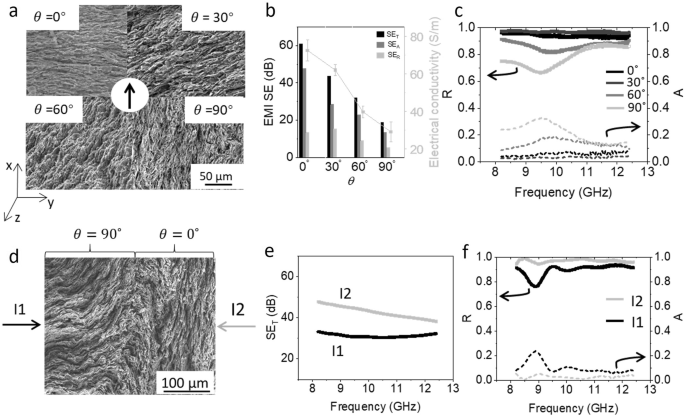
a Electron micrographs of cross-sections of the scaffolds with unidirectional microstructures at θ = 0°, 30°, 60°, and 90°. The arrow in the center indicates the direction of the incident EM wave along the x-axis. b SET, SEA, SER (bar data) and electrical conductivity (gray points) of the scaffolds from (a). c Reflection (R, plain lines) and absorption (A, dotted lines) coefficients for different θ as a function of the EM wave frequency. d Electron micrograph of the asymmetric scaffold with two regions of the same thickness with θ = 90° and θ = 0°. I1 and I2 indicate the possible directions of incoming EM waves. e SET and (f) R (plain lines) and A (dotted lines) coefficients of the structure (d) for the incoming waves I1 (black) and I2 (gray).
By orienting the rotating magnetic field at set angles, scaffolds with unidirectional microstructures at angles of θ = 0°, 30°, 60°, and 90° can be effectively fabricated (Fig. 3a). The electrical conductivity of the scaffolds measured in the plane (yz) perpendicular to the incoming EM wave varied significantly with respect to the angle, as expected (Fig. 3b). The electrical conductivity reaches its maximum value of 74 S/m at θ = 0° and decreases to 29 S/m at θ = 90°. A decrease in the electrical conductivity with θ leads to a decrease in the overall EMI SE, likely by decreasing the impedance mismatch with air and therefore allowing deeper penetration of the incident EM waves20,21,29. The EM shielding decreases from 61 dB for the SET, 48 dB for the SEA, and 13 dB for the SER at θ = 0° to 18.7 dB for the SET, 13.4 dB for the SEA, and 5.3 dB for the SER at θ = 90°. To further clarify the shielding response resulting from the microstructure orientation, the reflection R and absorption A coefficients representing the portion of the EM wave being reflected and absorbed, respectively, are plotted in Fig. 3c. Interestingly, the scaffolds with a microstructure with a larger θ exhibited less reflection of the incident waves, allowing more waves to penetrate the scaffold and resulting in increased absorption and transmission and decreased relative permeability µr (Fig. 3c and SI Fig. S6). This phenomenon is further confirmed by calculating the skin depth δ. The microstructure at θ = 0° has δ = 0.35 mm at 8.2 GHz and δ = 0.28 mm at 12.4 GHz, whereas the microstructure at θ = 90° has a much greater δ = 0.87 mm at 8.2 GHz and δ = 0.71 mm at 12.4 GHz (see SI Table S1 for the calculated values). The total thickness t of the samples was fixed at 0.75 mm, and δ is the depth at which the signal is reduced by 1/e. Therefore, when δ > t, the EM waves are less attenuated and can penetrate through the sample and be transmitted (case θ = 90°). In turn, when δ < t, most of the waves are attenuated. Additionally, δ depends on the frequency of the incident EM wave with smaller δ and higher A at low frequency and larger δ and lower A at high frequency, which is consistent with the experimental results in Fig. 3c. Therefore, we can conclude that a larger fraction of the incident EM waves are reflected by our scaffolds when the microstructure is oriented at θ = 0°, leading to a lesser fraction of the waves passing through. Consequently, θ = 0° leads to a higher SEA and lower A. In contrast, the scaffolds with microstructures oriented at θ = 90° allow a larger fraction of the incident EM waves to penetrate, leading to a lower SEA, higher A, and more efficient EM wave transmission. These observations have not yet been reported by others and confirm our hypothesis, as shown in Fig. 120,40.
After understanding how unidirectional microstructures affect the EMI SE, more complex microstructures, such as bilayers composed of two different unidirectional microstructures, are expected to provide other interesting responses. Here, a scaffold with an asymmetric microstructure was designed and fabricated using the same process. The bilayer has two regions of the same thickness of 0.375 mm with unidirectional orientations at θ = 0° and 90° (Fig. 3d). The EMI SE is tested for incident waves penetrating the sample from the microstructure at θ = 90° (incident wave I1) and from the microstructure at θ = 0° (incident wave I2). As expected, the shielding performance is quite different depending on the incident wave orientation. A higher shielding performance is observed for an incidence of I2 with SET = 45 dB than for an incidence of I1 with SET = 32 dB (Fig. 3e). The calculations of R and A show that the incident waves along I2 undergo greater reflection and less absorption than the incident waves along I1 (Fig. 3f). This difference corresponds to what is observed for unidirectional structures. Although the reflection and absorption at the interface between the two microstructures are difficult to detect and measure experimentally, we can infer that there is also more reflection and lower absorption at the interface for waves penetrating along I2 than along I1. In comparison to our scaffolds with a unidirectional microstructure at θ = 90°, the asymmetric scaffolds exhibited greater R, lower A, and greater SEA values for incident waves along I1, likely due to reflections at the interface with the layer at θ = 0°.
The microstructures of our scaffolds significantly impact their EMI SE, providing great potential for modulating and improving their shielding performance. However, the scaffolds developed thus far have been tested only for EM waves incoming in a very specific direction. In real applications, EM waves may have multiple incidence angles, which demands a 3D-shaped package with a local microstructure. Since our experimental setup for EMI SE is only for a one directional wave, we continue to explore how the local microstructure in pillar arrays can shield against a one directional wave as a proof-of-concept.
Tailoring the EMI SE using micro/macrostructures
To demonstrate that micro/macrostructure design can significantly impact the EMI SE, we created pillar arrays with two different microstructures in the pillars. Using M-DIW and subsequent thermal treatment, we obtained a zigzag structure with defined dimensions. We assimilate this zigzag structure to a pillar array to induce multiple reflections of the incident EM waves within the zigzag. The microstructure in the pillars is controlled to be θ = 0° or 90°, while the base has a microstructure oriented at θ = 0° since it shows the highest EMI SE. The height and distance between the pillars are also varied to study their influence on the EMI SE (Fig. 4).
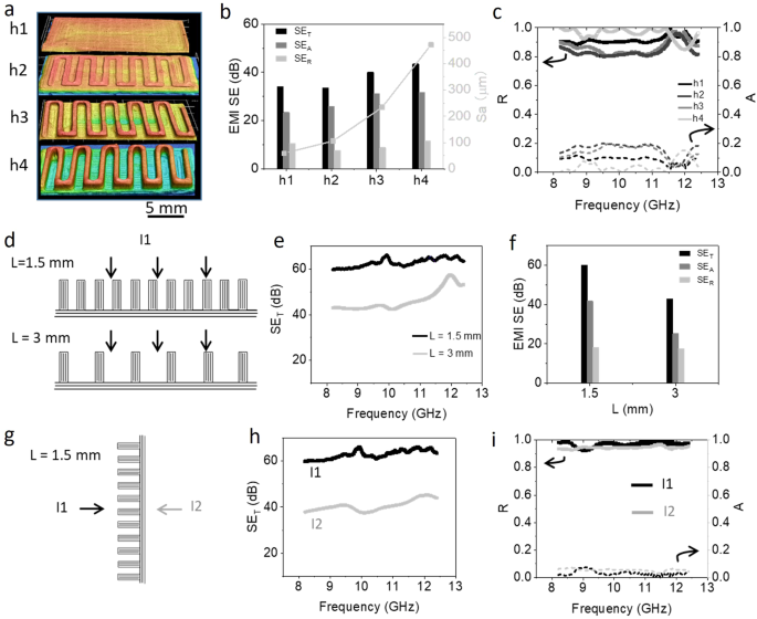
a Confocal images of microstructured pillar arrays with θ = 0° orientation throughout the base with a thickness of 0.5 mm (h1) and pillar arrays on h1 with pillar heights h2 = 0.25 mm, h3 = 0.5 mm, and h4 = 1 mm. b SET, SEA, SER (bar data) and surface roughness Ra (gray points) for the 4 pillar heights and microstructure θ = 0°, and (c) their R and A coefficients as a function of the frequency. d Schematics of the pillar array designs with the distance between pillars L = 1.5 and 3 mm and h3 = 0.5 mm, with the θ = 0° orientation in the base and θ = 90° in the pillars. e SET of the two arrays shown in (d) as a function of the frequency and (f) comparison of their SET, SEA, and SER. g Schematic showing the incident EM waves in directions I1 and I2 for the pillar array with θ = 0° orientation in the base and θ = 90° orientation in the pillars and L = 1.5 mm. h SET as a function of the frequency for the EM wave incoming directions I1 (black) and I2 (gray) on the structure in (g) and (i) associated R (plain lines) and A (dotted lines) coefficients.
Thanks to M-DIW, microstructured pillar arrays were printed with well-defined zigzag geometries (Fig. 4a). The microstructure of the pillars was effectively controlled (see SI Fig. S7 for electron micrographs). First, the height h of the pillars and the distance L between the pillars were tuned for an array with θ = 0° throughout the structure. Changing the height of the pillars on a base of thickness h1 = 0.5 mm while maintaining the same distance L = 1.5 mm changes the overall roughness of the structure. The surface roughness Sa of the pillar arrays with heights h1 = 0 mm, h2 = 0.25 mm, h3 = 0.5 mm, and h4 = 1 mm are 59, 106, 234, and 472 µm, respectively. The EMI SE of the pillar arrays increases with the height of the pillars or surface roughness, from SET = 34 dB, SEA = 23 dB, and SER = 11 dB for h1 up to SET = 43 dB, SEA = 32 dB, and SER = 11 dB for h4 (Fig. 4b). This increase in EMI SE can be due to the presence of more absorbing material but also to the geometry. The distance L was chosen to be smaller than the incident wavelength divided by 5, λ corresponding to 7.2–4.8 mm. Indeed, this condition of L < λ/5 has been reported to promote more reflection and scattering of EM waves in porous arrays24. Interestingly, the increase in surface roughness (h1 to h3) reduces the reflection coefficient R while enhancing A (Fig. 4c). This may result from the scattering of the EM waves and multiple reflecting events that promoted the absorption. However, a higher surface roughness (h4) results in increased R and decreased A, which must be due to multiple reflections occurring at the surface of the array. In principle, the absorption of EM waves increases as the surface roughness increases owing to the θ = 0° orientation of the mGr in the pillars. However, the results indicate otherwise. Close examination of the microstructure of the pillars revealed that within 30 µm of the edge of the pillar, the orientation of the mGr was θ = 90° (see the SI Fig. S8 for the electron micrographs). This misorientation is likely due to the shear forces that develop during the 3D printing process, which cannot be erased by the magnetic field, probably because the drying time at the edge of the pillar is faster than that at its center. Therefore, incident EM waves that are oriented perpendicular to the height of the pillar encounter a θ = 0° microstructure and are reflected. A low surface roughness sacrifices reflection, whereas a high surface roughness promotes reflection.
Since we attributed the increased EMI SE of the pillar arrays to the thin layer of the microplatelets with a θ = 90° orientation at the surface of the pillars, we consciously designed new pillar arrays with a microstructure oriented at θ = 0° in the base and at θ = 90° in the pillars for L = 1.5 mm and 3 mm and h1 = h3 = 0.5 mm (Fig. 4d).
These arrays achieve an SET of 60 dB, which is higher than that for the pillar arrays with θ = 0° throughout and with the same L and h, which is only 40 dB (Fig. 4b, d). Increasing the interpillar distance from 1.5 to 3 mm reduces the SET for pillar orientations at θ = 90° but still outperforms the arrays with pillar orientations at θ = 0° with the same L and h (Fig. 4e). Additionally, the SEA and SER of arrays with θ = 90° in the pillar and L = 1.5 mm are greater than those of arrays with L = 3 mm (Fig. 4f). These results suggest that the microstructure at θ = 90° in the pillar indeed induces multiple reflection and scattering events and reduces the wave penetration in the structure, leading to a higher EMI SE.
Furthermore, the pillar arrays are highly asymmetric and therefore interact differently with EM waves if their incidence is from the pillar side (I1) or the base side (I2) (Fig. 4g). The EMI SE of the arrays with θ = 90° in the pillar is greater for EM waves with incident direction I1, where SET = 60 dB, than for those with incident direction I2, where SET = 40 dB (Fig. 4h). R was also greater and A was lower for the I1 case (Fig. 4I). This further confirmed that the pillars in our scaffolds generated multiple reflections and scattering events, resulting in a high EMI SE.
The pillar arrays designed here have a base thickness of 0.5 mm, which is slightly greater than the skin depth (0.28–0.35 mm); however, the EMI SE is greatly improved by the multiple reflection events from the pillars because the pillars’ microstructure is oriented at θ = 90°, which is perpendicular to the incident waves reflected from the base. These results indicate that a well-designed micro/macrostructure can significantly tailor and improve the EMI SE. This approach is promising for creating high EMI shielding solutions that use less material and reduce costs; for example, for electronic packaging applications.
Microstructured composites for electronic packaging
Graphite is known to have high electrical conductivity and thermal conductivity and is low cost, anticorrosive, and hydrophobic. Therefore, graphite-based materials with excellent EMI SE could be used in various commercial applications, such as electronics. To meet the needs of electronic packaging materials, excellent thermal dissipation, high mechanical properties, and high stability and reliability are also required (Fig. 5).
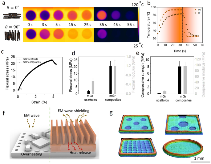
a Schematically aligned scaffolds with 0° and 90° orientations and infrared images during heating. b Temperature as a function of time during heating and cooling for the samples from (a). c Flexural stress‒strain curves of the scaffolds with unidirectional microstructures aligned at 0° and resin-infiltrated composites with the same microstructure and (d) their flexural strength (black) and modulus (gray). e Compressive strength (black) and modulus (gray) of the same scaffolds and composites. f Cartoon illustrating the application of micro/macrostructured composites for the packaging of an integrated electronic device to promote thermal dissipation and EMI shielding. g Confocal images of composites with different shapes.
To quantify the heat dissipation of the scaffolds, the heating and cooling of the scaffolds with unidirectional orientation at θ = 0° and 90° were evaluated. As expected from the anisotropic properties of graphite, scaffolds with microstructures aligned at θ = 90° heat significantly faster, reaching their maximum temperature in just 15 s, as compared to the scaffolds with θ = 0° that reached their maximum temperature after 25 s (Fig. 5a, b). The greater effectiveness of the vertical alignment of anisotropic microplatelets for thermal dissipation has also been reported in other works15. Therefore, rational design of the base and pillar in electronic packaging could promote heat dissipation in the future.
Furthermore, electronic packaging materials are also expected to physically protect electronics from the external environment. Owing to the high porosity of the scaffolds, commercial epoxy resin can fully infiltrate the pores using a vacuum to create composites (see SI Fig. S9a for the electron micrograph). The addition of the resin slightly reduces the EMI SE (SET = 56 dB instead of 60 dB), which may lead to a less pronounced impedance mismatch within the pores due to the presence of the resin instead of air (see SI Figs. S9b and S10 for the EMI SE of the composite and pure resin). The EMI SE performance of the composites is still very stable, with the SET remaining the same at room temperature and at 100 °C (see SI Fig. S9b, c). The infiltration of the resin markedly increased the flexural strength and modulus by 10 and 1.6 times, respectively, as well as the strain (Fig. 5c, d). The compressive strength and stiffness also increase by 36 and 10 times, yielding values of 8.1 and 97.4 MPa, respectively (Fig. 5e). The mechanical performances of the graphite scaffold and infiltrated polymer composites are comparable to those of other electronic packages15.
The excellent EMI SE, efficient heat dissipation and high mechanical performance of the composite guarantee the reliability and stability of the encapsulated electronic devices, as illustrated in Fig. 5f. The pillar design improves the EMI SE and can also act as a heat sink. Various electronic packaging shapes with controlled microstructures can be realized on demand using M-DIW, providing possibilities that other methods cannot achieve (Fig. 5g). Overall, these findings highlight the versatility of our micro/macrostructured composites and their ability to provide efficient and stable EMI SE, heat dissipation, and mechanical protection, making them promising materials for electronic packaging applications.
Conclusion
This study demonstrates the successful fabrication of highly dense micro/macrostructured graphite-based materials using M-DIW, which is a facile and easily tunable method that uniquely enables the fabrication of such delicately structured materials. The local microstructure precisely controls the EMI SE by varying the local electrical conductivity and impedance mismatch. Orienting graphite perpendicularly to the direction of propagation of the incoming EM wave results in high reflection, whereas a parallel graphite orientation leads to more penetration of the wave into the material. Considering this unique phenomenon, a proposed micro/macrostructure design with pillar arrays further increases the EMI SE by promoting multiple reflection and scattering events, improving the SET by 50%. The asymmetric design for packaging special components in electronics allows signal transmitters not only to emit efficiently but also to be protected from undesirable external EM waves.
In addition to the EMI SE, the material exhibits high heat dissipation, which can also be tailored by microstructural design. These properties make our materials promising for electronic packaging applications, especially after infiltration with a resin to increase the mechanical properties. The micro/macrostructural design proposed here applies to other 2D electrically conductive nanomaterials that may have even higher performance, such as MXenes, and the designs may be optimized using numerical simulations before being realized using M-DIW. In summary, the micro/macrostructural approach enabled by the M-DIW 3D printing method represents a significant advancement in the EMI field and provides a simple, customizable, low-cost, stable, and reliable solution for future high-performance electronic packaging.
Methods
Details on the materials and characterization are provided in the Supplementary Information.
Preparation of magnetized graphite microplatelets (mGr)
Two grams of graphite dispersed in 20 ml of ethanol was ground by ball milling (Retsch PM 100, milling balls with diameters of 5 mm and 3 mm) at 500 rpm for 4 h and for 5 min with a 2 min break to decrease their size and generate oxygen groups on their surface. After ball milling, graphite microplatelets with a thickness of 100–300 nm and a lateral size of 1–12 µm were obtained. After filtering, the ball-milled graphite microplatelets were redispersed in water, and the diluted ferrofluid was added dropwise (EMG 605, 3.9% vol). The solution was allowed to stir for 3 days. After filtering out the water, the obtained magnetically functionalized graphite microplatelets (mGr) were washed with distilled water and ethanol before being freeze-dried (Martin Christ/Alpha 2–4) and subsequently baked in an oven at 48 °C .
Ink preparation
A 4 wt% aqueous suspension of fumed silica was prepared and dispersed in a planetary centrifugal mixer (Thinky ARE-250) at 2000 rpm for 10 min. Afterward, the 10 wt% mGr was dispersed in the 4 wt% silica aqueous suspension and mixed at 2000 rpm for 10 min, followed by stirring for at least 3 days with a magnetic stirrer. Fumed silica was added to the aqueous suspension as a rheology modifier and dispersant to improve the dispersion of the mGr.
Magnetically assisted slip casting (MASC)
The ink was poured into a plastic mold placed on a porous gypsum substrate. A commercial neodymium magnet (60 × 20 × 10 mm3) fixed on a motor (RS Components Pte Ltd) that rotated at approximately 2 Hz was used to orient the mGr along the plane of rotation. The position of the magnet was adjusted so that the magnetic field strength at the location of the sample was 60–100 mT (measured using a Gaussmeter Hirst Magnetic Instruments Ltd., GM08). After casting, the samples were dried at room temperature for 2–3 days.
Magnetic direct ink writing (M-DIW)
The M-DIW apparatus was composed of a commercial 3D printer (CREALITY Ender-3 V2, Learners Hub Pte Ltd.) and a neodymium magnet (60 × 20 × 10 mm3) fixed on a DC geared motor. The position and orientation of the magnet depend on the intended microstructure. A magnetic field strength of 60–100 mT was controlled by placing the magnet at a distance of 1 cm next to the tip of the nozzle. For printing, 5 ml of the ink was loaded into syringes equipped with needles (diameter: 0.6 mm, Nordson EFD) and inserted into the 3D printer. The CAD model was drawn using Rhinoceros 3D and sliced using Prusaslice. NC Viewer was used to adjust the G code to account for shrinkage during drying. The printing speed was 1 mm/s, the flow rate was 400%, and the printed thickness for each layer was 0.2 mm. The material was extruded by the motion of the piston of the printer, which was controlled by the flow rate. The printbed consisted of flat porous gypsum used to quickly jam and dry the ink during printing.
Reduction of the scaffolds
The scaffolds were reduced in a tube furnace (Protege XST split tube furnace) and sintered at 1050 °C and 1400 °C in argon for 4 h. The heating rate was set at 3 °C/min, the temperature was maintained for 4 h, and the furnace was cooled naturally.
Composite preparation
Five grams of epoxy resin (WEICON Casting Resin MS 1000) was diluted with 1 g of acetone and stirred using a planetary centrifugal mixer for 1 min before 1 g of curing agent was added and stirred for 1 min. Acetone diluted the resin, decreasing its viscosity and slowing its curing time. This allowed more resin to enter the pores of the scaffold before it became viscous. The scaffolds sintered at 1400 °C were immersed in the resin and placed in a vacuum oven (Thermo Scientific), and the acetone was volatilized at 0.101 MPa. After 1.5 h of treatment, the resin became very viscous, and the composites were removed and cured at room temperature for 3 days.


Responses