Near-field terahertz time-domain spectroscopy for in-line electrical metrology of semiconductor integration processes for memory
Introduction
In the mass production of metal oxide semiconductor field-effect transistors (MOSFETs), it is essential to monitor electrical defects that determine the reliability and performance of the chip, which is why electrical die sorting analysis is typically performed after the chip is integrated1,2,3. In recent high-volume memory semiconductor chips, as nodes are shrunk to less than 20 nanometers, layers become extremely thin or new materials with new properties are introduced4,5,6. As a result, the grain size of the layer material and the charge carrier behavior at the interface are more sensitive than ever before, which can affect the electrical performance of the integrated chip4,7,8. In order to ensure the quality of thin films or their interfaces, it is necessary to strengthen in-line monitoring of electrical properties immediately after the unit process. This is preferable to post-integration inspection, which often takes months and hinders rapid feedback to front-end integration processes. However, conventional in-line electrical characteristic monitoring methods are often limited for being applied to sample undergoing integration, as these samples can be damaged.
The most commonly used technique in industrial semiconductor manufacturing is to measure the sheet resistance (RS) of the top layer film immediately after the process using a four-point probe9,10. The measured RS reflects electrical characteristics such as activated dopant concentration and grain size of metal or polycrystalline silicon11. However, because the four-point probe must contact the sample surface, it cannot measure the cell area that actually determines device performance without causing damage while integrating the chip. Instead, the RS of the cell is estimated by measuring the nearby observation site (OS), which is a separate area for monitoring purposes. Because the OS has a planar stacked structure, while the cell has a three-dimensional structure in nanometers, the results measured from the OS may not accurately represent the cell. As a result, there is a risk of incorrect process control based on the RS measurement of the OS. With regard to the quality of the interface between the substrate silicon and the gate oxide film, monitoring methods that do not interfere with the mass production process have not been found. Non-contact capacitance-voltage (CV) technology using corona charges is considered a candidate method12,13. However, it is challenging to discharge the applied corona charge quickly, which can delay the time until the next process. In addition, an extra process is required to check that the corona charge has been sufficiently discharged, which slows down production speed. Another potential candidate for in-line monitoring is a technique that derives electrical properties by observing the ratio of chemical species at the interface using secondary ion mass spectrometry (SIMS)14,15. However, this method is also sample destructive, making it unsuitable for monitoring large numbers of samples. Nevertheless, SIMS is known to be useful for optimizing process conditions and is often required in the early stages of mass production, so the number of wafers in the middle of integration is sacrificed in order to use SIMS analysis.
Therefore, it is necessary to develop a measurement technique capable of observing electrical properties without sacrificing samples. Terahertz (THz) time-domain spectroscopy (TDS) is a suitable base technology for this purpose16,17,18,19. The THz frequency light source, with its wavelength range spanning hundreds of micrometers to several millimeters, occupies a unique position in the energy spectrum, lying above the wavelengths typically used in conventional spectroscopy. Its low energy range precludes the alteration of electronic quantum states, but is rather ideal for absorption by free charge carriers. Additionally, the THz frequency light source has a low absorption cross-section for most materials and high transmittance even for thin metal films19. Therefore, using spectroscopy in the THz region allows for non-contact, optical measurement of the electrical properties of materials. This provides advantages such as being non-destructive, reproducible, and fast compared to methods that require contact probes or destructive treatment to measure electrical properties. Furthermore, since a light source with high transmittance is used, THz spectroscopy can obtain an absorption signal from the Si base layer to the uppermost layer in a semiconductor structure with multiple stacks. The change in THz absorption not only indicates the conductivity of the layer itself, but also reveals the effects on semiconductor such as inversion and depletion at the interface between the gate oxide and the Si substrate20. Hence, THz transmission is ideally suited to serve as a foundational metrology technology, non-destructively monitoring both the sheet resistance of the thin film and the flatband voltage of the product. However, a drawback of this method is its inability to discern the origin of absorption within a multilayer structure. Additionally, due to the Abbe diffraction limit, the THz light source has a relatively large spatial resolution of several millimeters, making it unsuitable for monitoring memory device pattern wafers that require sub-50 μm spatial resolution21,22,23. To overcome these challenges, the application of near-field scanning optical microscopy (NSOM) technology using probes can be considered24,25,26,27,28. While NSOM, based on the scanning probe microscopy (SPM), can yield nanometer-scale spatial resolution, it is expected to entail high costs and maintenance time due to the complexity of the components, to consistently keep the facility in optimal condition.
Here, we have developed micrometer spatial resolution THz TDS as an in-line tool for monitoring the dynamic random access memory (DRAM) integration process. Using a near-field microprobe for THz detection, we have successfully reduced the spatial resolution to less than 10 μm, enabling the precise measurement of individual cell units or specific OS blocks of less than 50 μm on the integrated DRAM. In addition, a signal correction technique was developed to eliminate signal variations caused by the lower base layer, which is not of interest in the multilayer film stack. Multiple wafer demonstrations in a real production environment have proven that the non-contact near-field THz TDS can effectively replace contact-based RS measured with a 4-point probe for tungsten thin film during DRAM integration. In addition, we show that with THz TDS can be used to monitor the rapid thermal nitridation (RTN) process, which is used to reinforce the titanium nitride layer in the DRAMs. It was confirmed that it is possible to detect non-destructively that nitrogen caused by RTN penetrates the lower layer and reaches the gate oxide/Si substrate interface to change the threshold voltage of the device. As for the amount of nitrogen penetration, the SIMS analysis of the same wafer measured by THz TDS was compared to confirm the penetration difference of the actual chemical elements.
Results and discussion
Micrometer spatial resolution THz TDS
The developed in-line instrumentation, as shown in Fig. 1, is based on THz time domain spectroscopy using terahertz radiation in the 0.2–1.6 THz band, corresponding to a wavelength range of 190 μm–1.5 mm. This frequency range, while avoiding most of phonon modes in solid samples, interacts with and is readily absorbed by free carriers in thin films29, resulting in contrast in the transmitted signal. The configuration of the THz TDS with a near-field probe and the principle of the near-field detection are shown in Fig. 1a, b, with further details described in the Methods section. The microstructure of the THz near-field probe consists of a pair of electrodes patterned with low-temperature growth GaAs cantilevers24,27, as shown in Fig. 1b. When a pulse with a wavelength of 780 nm is applied to the space between the electrodes, the photoswitch is optically excited and free carriers are generated. When the THz wave penetrating the sample overlaps in space and time with the area of the probe where the carriers were generated, current flow through, allowing to read out the electrical signal at the probe’s metal electrodes. Since the metal electrodes are only a few microns apart, sub-wavelength spatial resolution is achieved in close proximity to the sample surface. To obtain a near-field signal from the top of a 700–800 μm thick wafer substrate, the THz wave travels from the back to the front of the wafer, bringing the microprobe close to the top surface of the sample, which is favorable for obtaining a signal from the last process to occur. However, it still absorbs THz waves from depths throughout the sample, so the signal is variably affected by ‘incoming baseline intensity’ influences from previous processes and the Si substrate itself. The distance between the sample and the microprobe is a few microns to a few hundred microns, allowing rapid scanning of the sample surface, unlike the NSOM method, which is based on SPM where the tip must be very close to the sample. This is advantageous for fast scanning of entire wafers, and we were able to acquire 11,300 data points in about 15 min to create a map of the entire 12-in. diameter wafer, as shown in Supplementary Fig. 1. The stability of the system’s light source and probe is high enough to be used in semiconductor manufacturing. As shown in Supplementary Fig. 2, there was less than 10% linear signal intensity attenuation after nearly 17 months of full-time operation without powering down.
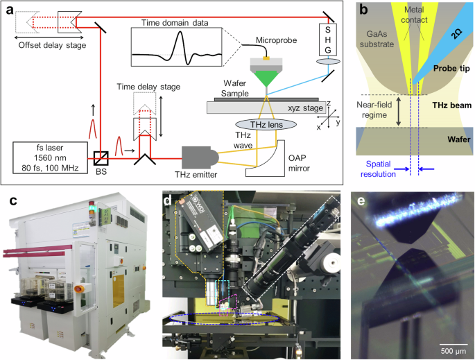
a Schematic optical setup of transmission-type THz TDS with microprobe for near-field detection. b Probe tip configuration and principle of achieving multi-micron near-field spatial resolution by the close distance between a probe tip and a wafer. c The developed in-line instrumentation system. It is configured to automatically lift and measure wafer carriers through the automated logistics system for high volume production line environments. d Main optical components for near-field measurement. Yellow grid line box indicates normal vision optics for wafer navigation and global alignment. Cyan grid line box indicates wafer height sensor. Magenta grid line box indicates microprobe for near-field detection. White grid line box indicates tilted view optics for fine alignment between probe and wafer. Blue grid line ellipse indicates a wafer being measured. e Tilted view image capturing the microprobe as it approaches the device wafer.
In near-field measurement techniques, the distance between the sample surface and the probe detector determines the signal intensity and spatial resolution, so the accuracy and precision of probe positioning is one of the most critical factors for performance30,31. Therefore, it is important to place the probe tip accurately and reproducibly in plane and height above the pattern spot to measure on any area of a large 12” diameter wafer. Typically, automated measurements for in-line metrology will move to coordinates that are specific to each device design layout in order to locate the desired cell block or OS on the wafer. However, it is often difficult to get directly to the desired location because the substrate wafer for memory semiconductors is not usually flat during the integration. As the wafer progresses to later processes, warpage and bowing are exacerbated by the increase in thin film stacking and thermal processes. Conventionally, this is solved by utilizing a vacuum-supported chuck to flatten the entire backside of the wafer, along with normal vision cameras, which is aligned normal to the wafer plane, and distance sensors for navigation realignment. However, our wafer chuck is uniquely designed to vacuum only three points on the wafer edge. This design minimizes the obstruction of the THz waves penetrating the wafer, but results in additional bowing and warping. Furthermore, as depicted in Figs. 1d and 2a, our system requires the normal vision camera and distance sensor for probe repositioning that cannot be situated atop the microprobe due to its cover, resulting in a discrepancy between the desired and actual position due to the warped wafer. This requires additional correction methods. We used a tilted vision camera to capture the probe, its reflection on the wafer, and the wafer pattern within its field of view, as shown in Fig. 1e32. Using the projection image derived from this tilted view, we successfully corrected the three-dimensional positioning of the probe.
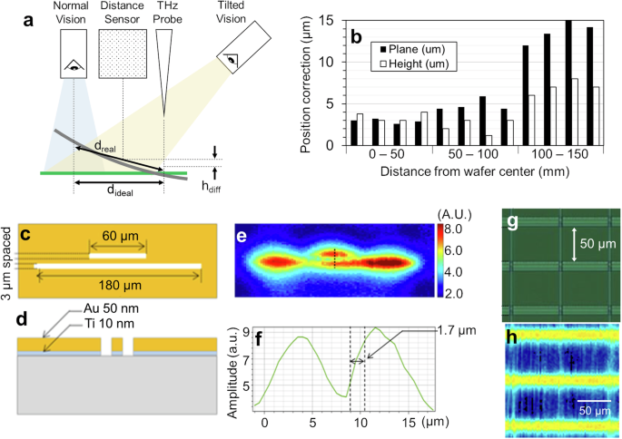
a Alignment system for the near-field microprobe on the patterned sample wafer. The curved gray line indicates an actual warped wafer, while the green line indicates an ideal flat wafer. b Additional position correction using projection image from tilt vision camera. Top (c) and cross-section (d) view of the sample pattern with dimensional information of the Au/Ti layer on the high resistive Si substrate. THz transmission image (e) of the sample and THz intensity profile (f) for the distance at the point indicated by the dotted line. Microscopic image (g) and near-field THz TDS transmission image (h) of cell block array of DRAM processed by Samsung Electronics.
As shown in Fig. 2b, for 12 measurement positions on a 12” diameter DRAM in-process wafer, we compared the difference in positioning accuracy between the conventional positioning method using the normal view and distance sensor and our proposed correction method using the additional tilt view. The difference between the two methods, additional position correction, increased from the inside of the wafer to the outside, and was larger for the distance in the plane than for the height. In particular, the larger difference as the wafer approaches the edge is obtained by the bow, warp, and tilt induced by the wafer support method and gravity33. The maximum difference between the two methods is 15 μm for planarity and 8 μm for height. For the height difference, a correction is found to be essential to account for the distance between the probe and the sample for near-field measurement.
The spatial resolution of the near-field THz TDS system utilizing our probe positioning method was verified using a test sample with a metal-based slit as shown in Fig. 2c–f. In the sample, the THz wave is absorbed in the area covered by the gold and titanium thin film layers, while it is highly transmitted in the area of the slit removed by etching, which clearly confirms the contrast in the image. When the dotted lines in Fig. 2e are plotted in Fig. 2f as a function of distance and THz transmission intensity, peaks and valleys in the signal profile due to the slit can be identified. The 20–80% range for the distance to a peak and valley is 1.7 μm, which corresponds to the spatial resolution of our system. Using this, when the cell block area of a DRAM with a width of about 50 μm is scanned with near-field THz TDS as shown in Fig. 2g, h, it is observed that the cell block area and the non-cell block area are clearly distinguished. This means that since our system can obtain signals only from the cell block, we can expect to obtain signals only from the area consisting of MOSFET structures. Thus, signals from other unnecessary areas can be excluded and reduced to various systematic errors in the measurement process. In addition, the quality of spatial uniformity within a chip can be checked with a minimum unit.
The proposed positioning method has been validated for precision using wafers from four different DRAM integration processes. The wafers from different processes show differences in the visual image due to patterns and in the overall area inhomogeneity due to warpage, especially in the later processes. To measure precision, statistics were obtained in two ways. In the static test, the wafer was placed on the stage and measured 30 times in a row. In the dynamic test, the process of placing the wafer on the stage and returning it to the carrier was repeated 10 times. The dynamic test is the overall precision of a system that includes features such as robots and motorized stages, which are different elements for finding the same location compared to the static test. The results are shown in Table 1. The maximum errors for the static and dynamic tests based on the planar axis are ±2.75 μm and ±2.96 μm, respectively. Meanwhile, the maximum errors for the static and dynamic tests based on the vertical axis are ±0.21 μm and ±0.34 μm, respectively.
Overall, the spatial resolution and precision results confirm that our system has sufficient sub-10 μm resolution. Although the tapered photoconductive probe we used does not achieve nanometer resolution, unlike the THz NSOM based on SPM, this is sufficient spatial resolution for patterned wafers of memory semiconductors. In fact, we believe that by avoiding the AFM or STM environment because nanometer resolution is not required, the system can be simpler, cheaper, easier to manage, and more robust. In the near future, as DRAM nodes continue to shrink, the size of the cell unit block and the OS block will shrink from their current size of about 50 μm. However, it can be seen that the sub-10 μm spatial resolution of the near-field THz TDS we have developed already has a generous margin for the smaller block area.
Non-contact measurement of thin film resistivity: Tungsten gate and contact
THz waves are sensitive to the charge carrier density of the material and have an excellent ability to measure the electrical properties of the metal thin film in a non-invasive way17,25. Because of these properties, many previous studies have been conducted to extract the electrical properties of graphene and conductive metal thin films using THz range34,35. In most of these previous studies, a high-resistance intrinsic silicon substrate was used to eliminate the effect of the substrate on the measurement. However, in actual semiconductor manufacturing, a base-doped p-type silicon wafer is used as the substrate, and it must be measured between several additional implants, thermal processes, and thin film deposition. This results in different absorption of THz waves in the substrate and in the layers stacked on top of it, depending on the individual wafer or the position in the wafer plane. For this reason, it is difficult to directly measure the unique sheet resistance only from the thin film of the top layer of interest. In general, to solve this problem, measurements are taken before the process of interest and used for incoming baseline intensity rejection, which results in low productivity as it requires two separate measurements before and after the process.
Therefore, we developed a correction method to eliminate substrate absorption from the signal intensity, requiring only a single post-process measurement. As shown in Fig. 3b, the incident THz light sources are aligned perpendicular to the wafer, resulting in not only primary pulses transmitted directly to the detector, but also echo pulses. These echo pulses internally reflect off the top layer surface, or nearby interface, and arrive at the detector with a delay. Given the additional travel time, primary and echo pulses can be distinguished in the time domain as shown in Fig. 3c. Taking into account the refractive index of Si, the time interval between the two arrivals is 17.6 ps, which corresponds to a round trip distance of 776 μm, the typical thickness of a Si substrate. In the case of multiple round-trips at Si substrate, it is excluded from the discussion because it is judged be not included in our time window. The transmitted intensity can be described as Tprimary for the primary pulse and Techo for the echo pulse transmitted by the single internal round trip, respectively, as the product of the optical properties as shown in the following Eqs. (1) and (2).
Here, ({t}_{{ij}}) is the transmission coefficient when THz waves are incident from medium i to medium j (0: air, 1: wafer), and ({widetilde{t}}_{{ij}}) refers to the transmission coefficient modified by the multistack of thin films over wafer substrate. Where ({r}_{{ij}}) and ({widetilde{r}}_{{ij}}) are reflection coefficients for THz wave reflected at the interface of two different media and at the modified surface, respectively. Note that the coefficients in the equations here are considered with multiple internal reflection on thin film layers. ({C}_{{{rm{geo}}}}), and ({C}_{{{rm{geo}}}}^{{prime} }) are constants corresponding to the fraction of THz waves actually reaching the probe due to the probe geometry for the primary and echo pulses, respectively. When the substrate is a silicon wafer having a complex reactive index of ({n}_{{Si}}^{* }) and a thickness of ({d}_{{Si}}) of 750–800 μm, Eq. (3) refers to a term in which a signal propagating through a silicon wafer on a transmission path has a value less than 1 due to the imaginary term of ({n}_{{Si}}^{* }) which varies with the doping concentration of the wafer. This term is the absorption term by the bulk Si substrate, which is a major factor of the incoming baseline intensity. Note that the propagation term appears only once in the case of the primary pulse, while it appears as a cube in the case of the echo pulse. Therefore, the propagation term can be eliminated by correcting ({T}_{{{rm{primary}}}}) by ({T}_{{{rm{echo}}}}) as described in Eq. (4), leaving ({widetilde{t}}_{10}), ({widetilde{r}}_{10}) associated with the upper thin film of interest.
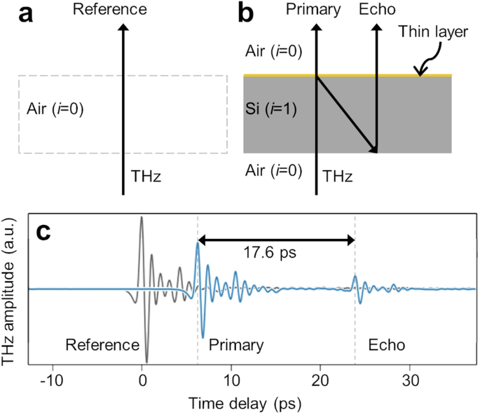
a Reference signal transmitted through air. b Two signals transmitted through the wafer. The primary pulse is the one that passes through the sample and arrives directly at the detector, and the echo pulse is the one that is reflected at the top surface of the Si substrate and travels once inside the Si before arriving at the detector. The gray area is the Si substrate, and the yellow line is the new layer formed by the process. c Transient signal of THz pulses transmitted through air and silicon wafer as gray and blue solid lines, respectively. When the time difference between two pulses through the Si wafer is twice the thickness of the wafer, the late-arriving pulse is an echo that has made a round trip inside the Si.
Utilizing Eq. (4), we were able to effectively suppress incoming baseline intensity by correcting the THz transmission obtained from the tungsten film in the DRAM processes. This was assessed across three different tungsten layer deposition processes, which are the buried channel array transistor (BCAT), the direct contact to cell (DCC), and the direct contact (DC) located between the DCC and the capacitor, respectively. We measured the THz TDS and 4-point probe RS at the same location on the OS after tungsten deposition. The multistack structure of the OS of each process has different incoming baseline intensity because the OS is configured differently, as shown in Fig. 4a, d, g. In addition, each measured wafer was from different carriers, which are likely to have different incoming baseline intensity. When comparing the linear correlation between the uncorrected and corrected THz transmittance and RS, as shown in Fig. 4 and Table 2, significant differences were observed. The determination coefficient of the correlation, R2, increased significantly to 0.90–0.98, nearing 1, when corrected, as opposed to 0.35–0.84 when uncorrected. Different colored dots in Fig. 4b, e, and h show different linear relationships, indicating variation in incoming baseline intensity between wafers from different carriers. However, the corrected signals, regardless of the dot color, showed a single linear relationship with RS in all cases as shown in Fig. 4c, f, i, implying the effective removal of incoming baseline intensity between wafers.
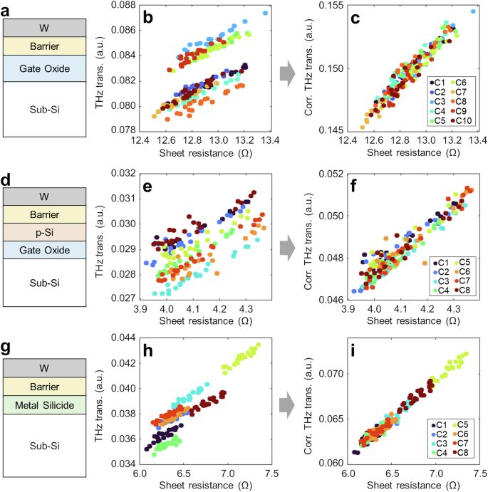
The positions used to measure the wafers are shown in Supplementary Fig. 3a. Tungsten layers for a–c buried channel array transistor (BCAT) process, d–f direct contact to cell (DCC) process, and g–i tungsten layers for direct contact (DC) process above DCC but below capacitor. a, d, g For each process, the OS is shown in a multi-stack configuration with tungsten shaded in gray, barrier layer in yellow, gate oxide in blue, polycrystalline silicon in orange, metal silicide in green, and substrate Si in white. THz transmission analysis results from the primary pulse for three different tungsten deposition steps during the DRAM integration process (b, e, h) and the analysis results corrected by the echo signal (c, f, i). Each measured wafer was selected from different 8–10 carriers for each process, and each carrier, which is likely to have a different incoming baseline intensity, is shown as dots of a different color. Same colored dots indicate the same wafer only if it is the same process among three.
It is important to note that the above results are not a deliberate broadening of the resistivity of tungsten by controlling process conditions on the sample for evaluation purposes, but rather a naturally occurring process distribution for a product that already has a high yield of over 90%. This indicates that the near-field THz TDS method we have developed for monitoring metal thin-film processes has advanced beyond proof-of-principle and can serve as a viable alternative to the conventional four-point probe method. The use of four-point probes requires physical contact with the sample and, as a result, leads to rapid wear and high maintenance costs. Conversely, the non-invasiveness of near-field THz TDS makes it an attractive method for measuring resistivity, as it provides fast and reliable statistics with relatively low maintenance costs. It is also important to note that while the four-point probe is destructive and can only measure the OS, our near-field THz TDS can measure the cell area where the actual MOSFET structures are formed, as the electrical environment in the complex nanostructures of the cell area may differ from the simple planar layered structure of the OS. However, the structures that make up the cell are no longer planar layers like the OS, so the direction of the THz waves that penetrate them may be different, making it difficult to apply the calibration method presented above. Therefore, new calibration methods may be required or measurements before and after the process may be necessary. In addition, it is worth noting that wafers that have undergone THz TDS measurements have subsequently been integrated into actual products without any problems during the remainder of the manufacturing process.
An important note is that while the calibration in Eq. (4) worked successfully for all three different multistacks, the linear regression equation between RS from the four-point probe and the THz transmission is not a universal model and requires optimization for each individual process as shown in Supplementary Fig. 4. This is because the calibration method we present focuses on removing most of the factors contributed by the Si substrate, which may leave some of the signals from the layers between the uppermost and the Si substrate layer, such as barrier or gate oxide, as seen in Fig. 4a, d, g. The signals from these underlying thin film layers may not be fully compensated due to different environments for their respective process steps. Therefore, to obtain an optimized regression model for each process, the reference RS must be measured in preparation for calibration.
Non-destructive interface monitoring: rapid thermal nitridation process
In THz TDS, THz waves are absorbed not only by the bulk, but also by the interface between the underlying films, resulting in a noticeable difference in transmittance. Taking advantage of this, we have used THz TDS to monitor the properties of the interface between the underlying films, which changes after the subsequent thermal process. In MOSFET structures, the titanium nitride (TiN) layer often plays an important role between the tungsten metal gate and the SiO2 insulating layer. Tungsten is an appropriate choice for a metal gate in both DRAM and 3D NAND flash memory due to its superior step coverage that gradually increases the aspect ratio36,37, however, a TiN barrier layer is primarily required underneath. This is because the TiN layer functions as an adhesive layer for tungsten deposition on the sub-SiO2/Si layer and as a diffusion barrier to prevent the WF6 reaction38,39,40. To enhance the barrier performance of the TiN layer, the N:Ti ratio is amplified by an additional nitridation process immediately following plasma enhanced atomic layer deposition (PE-ALD) deposition, which enhances the TiN into a denser layer. This is achieved by rapid thermal annealing in an N2 atmosphere with ammonia. However, as the dimensions inevitably shrink for high-density memory chips, the N from ammonia or N2 gas applied during rapid thermal nitridation (RTN) easily penetrates the thinned SiO2 layer, reaching the Si substrate. In particular, ammonia penetrates SiO2 to form a [Si–N–O]+ cluster to form a fixed charge, and nitrogen absorbed by SiO2 is diffused and deposited at the SiO2/Si interface41,42,43,44,45. As a result, the increased fixed charge near the interface applies an additional electric field to the Si of the interface region corresponding to the carrier channel, and the threshold voltage (Vth) changes45,46,47. Therefore, it is necessary to monitor the amount of nitrogen accumulation at the SiO2/Si interface after the nitridation process.
The ability of THz TDS to detect differences in interface due to nitrogen infiltration was evaluated using wafers processed in a DRAM process that underwent RTN at three different temperature conditions. Prior to RTN, the standard processes for sub-20 nm node DRAM product were applied, which typically includes the deposition of the TiN layer during the BCAT structure fabrication phase. The RTN process was then performed on three wafers at temperatures of 670, 700, and 730 °C, respectively. The THz signal was recorded from two types of OS forming a planar multilayer structure on five chips located near the center of the patterned wafer. As shown in Fig. 5a, d, the layered structure of the OS has an amorphous silicon dioxide layer, which is the gate oxide, on a Si substrate using boron as the base doping, and a TiN layer on top. The thickness of the SiO2 layer is ~100 Å for OS1 and ~500 Å for OS2, showing a large difference in thickness between the OSs. To confirm the absolute amount of nitrogen components that penetrated to the SiO2/Si interface as measured by near-field THz TDS, the device integration of the wafer was terminated immediately after the THz TDS measurement and exported from the production line to undergo destructive SIMS analysis to confirm the profile of silicon nitride based on depth. Analysis results could only be obtained from one chip in the center of the wafer due to the difficulty of cutting the wafer into coupon samples for SIMS measurement. Silicon nitride (SiN) was detected as the nitrogen species for SIMS analysis, as it is expected to be formed by the intruded nitrogen combining with Si from SiO2 or Si substrate. As a result, Fig. 5b, e are depth profiles for SiN species from different OSs, respectively. For OS1, which has a thinner gate oxide, nitrogen penetration to the SiO2/Si interface varies noticeably with RTN process temperature. However, for OS2, which has a thicker gate oxide, it is confirmed that the difference at the interface is indistinguishable. When the SiO2 thickness is less than 100 Å, nitrogen penetration to the SiO2/Si interface is noticeable and this difference can be easily confirmed by SIMS analysis42. However, when the thickness of SiO2 is greater than 100 Å, the nitrogen penetration is minimal, resulting in an inability to distinguish between samples with SIMS analysis sensitivity.
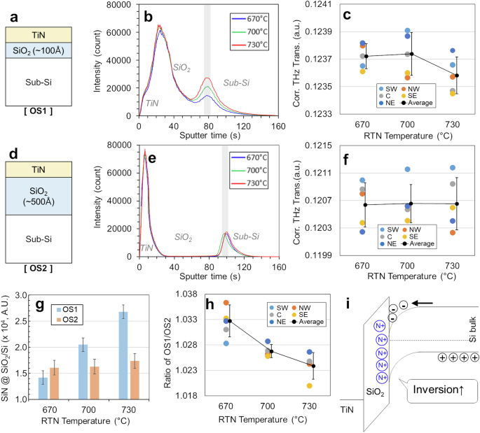
The positions used to measure the wafers are shown in Supplementary Fig. 3b. a, d The film stack composition at each observation point (OS) is shaded yellow for TiN, blue for SiO2, and white for substrate silicon. b, e Secondary ion mass spectrometry (SIMS) result on two OS after RTN at 670–730 °C as blue, green, and yellow solid lines, respectively. g Amount of SiN at the SiO2/Si interface measured by SIMS. It is highlighted as a shaded area in (b,e) where the data for the interface region were used. The average of the values in the shaded area from b, e is used as the bar value as blue and orange bars of OS1 and OS2, respectively, with the standard deviation shown as a black error bar. c, f, h Correlation of THz transmission with SiO2/Si interface nitrogen accumulation as a function of RTN process temperature. The results of five points measured at the center, southwest, northwest, southeast, and northeast of the wafer are shown as gray, light blue, orange, yellow, and navy dots, respectively. The average of the five points is shown as a black dot, with the standard deviation shown as a black error bar. i Proposed model of THz transmission intensity reduction due to Si inversion induced by positive fixed charge on SiO2 near the interface.
In the case of THz transmission, however, the differences in RTN temperature cannot be distinguished from the corrected signal intensity using Eq. (4) in both OS, as shown in Fig. 5c, f. Although a weak tendency for THz transmission to decrease with increasing temperature is observed in OS1 with relatively thin SiO2, the reliability is very low when considering the distribution of five chips. This is because Eq. (4) is inadequate for cases where the SiO2/Si interface is actually in the substrate, since it is designed to preserve information from the top multistack but eliminate signals from the underlying Si substrate. In addition, the interface is typically only about a nanometer thick43, which is much finer than the thin film itself, so the volume that makes a difference in the signal is very small. In particular, due to the large signal variance caused by TiN layers, which have good electrical conductivity48, the absorption signal in the ultrathin interface region can only be distinguished by canceling out the absorption in the TiN layer. Therefore, an alternative correction method as follows is necessary to see the difference at the SiO2/Si interface.
We took advantage of the fact that the amount of nitrogen accumulated at the SiO2/Si interface as a function of RTN temperature is considerably different between OS1 and OS2. When Eq. (3) is decomposed into Eq. (5), which represents the absorption of the Si substrate, the term can be divided into a bulk region, which is far from the top layer and therefore hardly affected, and an interface region with a thickness of δ, which is strongly affected by the top layer. Then, by dividing the THz transmission of OS1 by OS2 as in Eq. (6), the terms related to the TiN layer and the bulk region of the Si substrate are canceled out, leaving only those for the SiO2/Si interface and SiO2. In the case of SiO2, ({widetilde{t}}_{10}) partially remains after dividing the transmission signal between OS1 and OS2 due to the different thicknesses of SiO2 at each OS. However, unlike Si in the interfacial region, the THz transmission of the insulating layer, SiO2, does not vary with temperature, and it is assumed that there is a small fixed absorption difference due only to the thickness difference. Therefore, although omitted in the notation, the absorption difference between OSs on SiO2 is a constant in the relationship in Eq. (6). As a result, by using Eq. (6) as a correction method, a THz transmission can show the difference in nitrogen penetration to the SiO2/Si interface as shown in Fig. 5F, where the difference in THz transmission is more apparent than the distribution of five chips for each RTN temperature. To detect differences at the interface in this way, a method using signal correction between closely spaced OSs with different stack thicknesses or layer configurations is considered a valid correction method in memory semiconductor metrology. OSs under different conditions must be correctly paired, as different types of byproducts are expected to remain in order to monitor the effects of each process.
As shown in Fig. 5F, the corrected THz transmission decreases as the amount of nitrogen at the interface increases, according to the results of the inter-OS correction. As ammonia penetrates at the SiO2/Si interface, a positive fixed charge of nitrogen species accumulates in the SiO2 near the interface44,45,46,47,49. This positive charge adds an extra field to the interfacial Si and attracts electrons, which are minority carriers in the boron-doped Si substrate. The increased population of electrons on the Si substrate near the interface subsequently generates an inversion. This inversion intensifies with the increase of the fixed charge from the infiltrating nitrogen. Consequently, an increase in free carriers near the interface can be expected, which subsequently leads to an increase in THz absorption. Previous research has shown that stronger inversion, induced by increasing the field applied through the electrode to the MOSFET structure, results in greater observable THz absorption20. In addition, the microwave loss of a metal/SiO2/Si stacked structure has been shown to be due to an inversion caused by a positive charge gate oxide near the interface; since the microwave is a region of lower THz wavelength, the change in absorption can be considered to follow the same principle50,51,52.
In-line monitoring technology for specific interfaces is critical but still uncommon. Various technologies including XPS, XRF, FTIR, Corona CV and SIMS have been tried to monitor nitrogen penetration in the RTN process, each with limitations. As a result, typical analytical techniques are not suitable for implementation in the middle of the integration process. In particular, XPS, which is commonly used to monitor the Ti:N ratio to control RTN process parameters, only assesses the performance of the TiN layer as a barrier due to its limited penetration depth. It is unable to predict changes in Vth caused by the accumulation of nitrogen in the lower layer or lower interface. In addition, XRF and FTIR are unsuitable for measuring patterned wafers due to their large measurement spot size, while non-contact CV using corona charging or SIMS, which cannot restore the wafer state after measurement, are unsuitable for the in-line measurement process. Therefore, THz transmittance is currently the only viable method for these processes.
Methods
Near-field THz TDS
The optical elements for THz generation and measurement were constructed using components supplied by Protemics GmbH and were augmented with modules for stabilizing both the pointing and power of the beam to ensure the long-term stability of the system. As shown in Fig. 1a, the THz TDS system is a classical pump/probe scheme based on a fiber-based femtosecond laser with a center wavelength of 1560 nm and a pulse duration of 80 fs. The femtosecond laser is used to optically excite a photocurrent THz emitter and a near-field THz microprobe (Protemics GmbH TeraSpike). The emitted laser beam is split by a beam splitter into a THz emitter path and a probe beam path, and the emitter-side path beam is passed through a motor stage that repeats high-speed round-trips without stopping for fast time-delay scanning. The pump beam directed to the THz emitter is then focused to ~20 mW. The emitter is an InGaAs/InP photodetector with a stripline antenna biased at 100 V to provide a bandwidth of 6 THz and an average power of 30 μW. The generated THz radiation is collimated by an off-axis parabolic mirror, focused on the device wafer by a lens, and then transmitted to the probe. Meanwhile, the probe-side beam passes through a time-compensated delay stage to a second harmonic generator (SHG) module, where the beam undergoes wavelength conversion from 1560 nm to 780 nm (2Ω). The generated 2Ω beam is focused onto a low temperature growth GaAs probe to excite the probe tip and generate photocarriers. At the probe tip, a THz electromagnetic field that overlaps in space and time with the 2Ω beam accelerates the photocarriers and generates a measurable current. This current can be measured via metal electrodes at both ends of the probe antenna, as shown in Fig. 1b. Since the measured current is proportional to the amplitude of the transmitted THz wave, it measures the field intensity of the THz wave. The time domain spectrum is obtained by rapidly sampling the time delay between the THz wave and the detector beam. The optical delay of the pump and probe beams is swept in steps of 0.05 ps in the range of 0–50 ps, and the THz waveform is collected in the corresponding time domain. The chuck holding the device wafer for measurement is evacuated at three points on the edge of the wafer, while the rest of the wafer area is open and transparent to THz waves.
Probe positioning method
Using a vertical optical system with 10x magnification and a camera pixel size of 0.48 μm, information about the Cartesian coordinates of the wafer center and the rotation axis of the wafer is checked as the motorized stage moves. This information is used to obtain the primary calibrated Cartesian coordinates for the stage to locate the desired position. A distance sensor with 100 nm repeatability is used to measure the distance between the wafer surface and the probe and to perform coarse approach. We have newly devised a method for positioning the probe and surrounding pattern using an image from a separate oblique optical system, as shown in Figs. 1d and 2a. This system is employed to perform both a fine approach, achieving a sub-10 μm distance between the wafer surface and the probe, and a secondary calibration of the position.
Sample preparation and measurement
As shown in Fig. 2c, d, a test sample for verifying the spatial resolution of our near-field THz TDS was prepared by depositing 50 nm thick gold and 10 nm thick titanium on a 500 μm thick high-resistivity silicon wafer, and the short and the long slit regions, each 3 μm wide and separated by 3 μm, were removed by etching. THz transmission images are obtained by the scanning method shown in Supplementary Fig. 5. The distance between the sample surface and the probe is kept at 2 μm, and then the probe is slowly moved to scan a rectangular area of 200 × 50 μm2.
In the case of the tungsten film evaluation, measurements were performed on three different tungsten deposition processes during DRAM integration at sub-20 nm nodes. The tungsten for the buried channel array transistor cell structure was deposited by atomic layer deposition (ALD) of B2H6 and WF6 to form a tungsten seed layer, followed by chemical vapor deposition (CVD) of WF6 and H2 to form a bulk tungsten layer. The tungsten layer for the direct contact cell (DCC) structure was formed by physical vapor deposition. The tungsten for the direct contact (DC) structure was formed by ALD of SiH4 and WF6 to form a base layer, followed by CVD of WF6 and H2 to form a bulk tungsten layer. The measured wafers were selected from 8 to 10 random carriers per process, each represented by different colored dots in Fig. 4. The wafer measurement position is shown in Supplementary Fig. 3a.
Measurements were performed on TiN samples for RTN process to reinforce TiN film as barrier metal for BCAT structure generation during DRAM integration at sub-20 nm nodes. TiN thin films were deposited by PE-ALD using tetrakis(dimethylamido)titanium and N-radical. RTN was performed at temperatures of 670, 700, and 730 °C with NH3 in N2 atmospheres, respectively. The wafer measurement position is shown in Supplementary Fig. 3b.
THz transmission
The basic signal processing of the measured transmission was calculated as follows. The transmittance, T(ω) = Asample(ω)/Aair(ω), was obtained after reshaping with a Gaussian pulse with a center frequency of 0.505 THz and a fractional bandwidth of 0.98 THz, based on a range from the lower frequency of 0.01 THz to the upper frequency of 1.0 THz. Then, the transmittance values in the range of 0.3–0.7 THz were taken as the geometric mean and used as the representative THz transmission value at that measurement location. In this way, the arithmetic mean and standard deviation of the transmission values in the OS1 (or OS2) region at the five locations on the wafer were used for analysis.
Responses