Non-Hermitian selective thermal emitter for thermophotovoltaics
Introduction
TPV systems convert heat to electricity via light (Fig. 1a), unlike thermoelectric systems2. The intermediate optical step in the overall energy conversion scheme allows the TPV scheme to decouple the optimization of its thermal and electrical parts. This separation makes optimizing the TPV scheme for high efficiencies easier than optimizing the thermoelectric scheme. Thus, TPV is considered promising for efficient solid-state heat-to-electricity conversion3. In the TPV scheme, a low-band-gap photovoltaic (PV) cell absorbs thermal photons from a hot emitter to generate electricity. Without controlling the spectral spread of the thermal photons from the hot emitter, the TPV efficiency is low. However, suppressing the emission of photons with an energy smaller than the PV cell’s bandgap (Eg) can greatly boost the TPV efficiency. This spectral engineering can be achieved in two different ways: photon recycling in a cavity4,5,6,7,8,9 and selective thermal emission10,11,12,13,14. While photon recycling requires a high-quality optical cavity for sub-bandgap photons, selective thermal emission requires an engineered hot emitter. Both approaches have advantages and limitations and are sought for specific applications. Generally, low- and medium-grade heat sources benefit from the latter approach, while the former is promising for high-temperature (> 1500 K) sources. Here, we focus on low- and mid-grade heat conversion applications, such as waste heat recovery, and consider the selective thermal emission scheme.
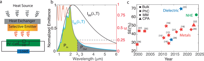
a Schematic showing a TPV power generator with a heat exchanger, selective thermal emitter, and a photovoltaic cell to convert heat to electricity via thermal radiation. b Spectral emissivity (right vertical axis) of a typical selective emitter (red curve) and the corresponding spectral emittance (blue curve, left vertical axis) along with the spectral emittance of a blackbody at the same temperature (black curve). Considering the bandgap or the absorption edge of the PV cell (λc) aligns where the emissivity crosses value 0.25, the optical power emitted for photon energies above the bandgap (Pin, shaded in green) can be converted to electricity by the PV cell. However, the power emitted in the sub-bandgap spectrum (Pout, shaded in gray) is not absorbed by the PV cell and hence is lost. c Spectral efficiency (SE) values were calculated (see materials and methods) using reported high-temperature emissivity data of selective emitters based on bulk, photonic crystal (PhC), metamaterial (MM), and coherent perfect absorption (CPA) designs. The red and blue colors represent metal-based and entirely dielectric designs, respectively. The green circle shows the SE of our hybrid metal-dielectric non-Hermitian emitter (NHE).
In the selective thermal emission scheme, the heat exchanger surface is covered by a selective emitter, as shown in Fig. 1a. The selective emitter emits thermal photons not like a blackbody but with higher probability in the desired super-bandgap region (see 1b). In other words, the emissivity of the selective emitter is high (nearly unity) in the desired super-bandgap band and low (ideally zero) in the sub-bandgap region. The higher the contrast of the selective emitter, the greater the efficiency of the TPV system. Hence, an appropriate performance metric for the selective emitter is its spectral efficiency or SE10, as defined in Eq. (1)
where ISE(E, T) represents the spectral emittance of the emitter given by the product of spectral emissivity (ε) of the emitter and blackbody spectral emittance (IBB) at temperature T (see Fig. 1b).
High spectral efficiency can be achieved by selectively enhancing the emissivity in the desired energy range (Eg to Eg + ΔE) while suppressing it outside this range. The long tail of the blackbody emittance at longer wavelengths makes it essential to have low emitter emissivity in the wide band below Eg15,16.
Common bulk refractory metals, such as tungsten and tantalum, suppress thermal emission in the long sub-bandgap region in the IR and serve as selective thermal emitters17. Adding nanophotonic cavities onto the surface of this refractory metal increases emissivity in the desired spectral window while maintaining it low in the sub-bandgap region. Nanophotonic cavities such as photonic crystals (PhC)18,19,20,21,22, metamaterials (MM)23,24, and coherent perfect absorbers (CPA)25 based on metals have been well studied as selective thermal emitters. We calculated the SE of these designs available in the literature using a common set of rules (see the section Materials and Methods). Figure 1c plots the estimated SE of metal-based selective emitters in red. The SE value ranges from 30–50%. These metal emitters are preferred in many applications despite their moderate SE because metals make excellent heat exchangers. Metals conduct heat well from the source to the emitting surface while blocking any thermal photons that leak through them from the source26. Thus, metal-based selective emitters are useful.
In contrast, dielectric materials remain almost lossless (implies low emission) in the sub-bandgap region at elevated temperatures27 and are promising for high SE28,29. However, the dielectrics remain transparent in the sub-bandgap region and allow thermal photons from the source to leak into the PV cell. Thus, dielectrics alone make bad heat exchangers. For all practical purposes, dielectric emitters need a metallic substrate as a heat exchanger. The thermal emission from this metallic substrate would then pull down the SE of the dielectric/metal substrate system.
This limitation in conventional selective emitter design could be overcome by designing a hybrid metal-dielectric system, where the metallic component acts as a heat exchanger and generates thermal photons while the dielectric material provides a high-Q resonant mode to achieve the desired spectral selectivity. This functionality is easily achieved in non-Hermitian thermal emitters30,31 with coupled plasmonic and dielectric resonators. When weakly coupled, high absorption loss in the plasmonic resonator efficiently generates thermal photons that are stored in the high-Q dielectric resonator, resulting in good spectral selectivity.
Here, we report the design, fabrication, and testing of a hybrid metal-dielectric non-Hermitian emitter (NHE) that promises a spectral efficiency exceeding 60% (Fig. 1c). We experimentally show that the emitter maintains its high spectral selectivity at 1273 K under vacuum with minimal degradation. Furthermore, we build a complete TPV system, demonstrate its operation, and measure its conversion efficiency η.
Results
Design for the non-Hermitian selective thermal emitter (NHE)
Our selective thermal emitter is designed to exploit the non-Hermitian behavior of thermal emitters. Though all thermal emitters are non-Hermitian systems or open systems, their design in the past did not benefit from this quantum description. Our work30 was the first one, to the best of our knowledge, to employ a non-Hermitian framework to design selective thermal emitters. This non-Hermitian selective emitter was based on coupling a dielectric dipolar mode to its lossy image in a tungsten ground plane. When the two modes were weakly coupled, the system supported two modes with very different damping rates. The heavily damped mode controlled the thermal emission brightness, while the lightly damped mode controlled the Q-factor. This allowed our emitter to be simultaneously bright and selective, an impossible feat otherwise due to an inherent trade-off. Here, we build upon this past work to design a non-Hermitian selective thermal emitter for TPV applications. Here, additional considerations—bandgap of the PV cell, emission band of the emitter, operating temperature, and thermal stability of the materials and nanostructures of the design—constrain our design. A rational choice of the design parameters led to the following design of our selective emitter.
Our selective thermal emitter is designed on an optically thick tungsten substrate (0.5 mm) that serves as a plasmonic material as well as a heat exchanger. We designed cylindrical silicon resonators on a SiO2 dielectric spacer on the tungsten substrate as shown in the schematic of Fig. 2a. The silicon nanodisks are 500 nm in diameter and 250 nm tall, making a hexagonal lattice with nearest neighbor separation of 1220 nm. This specific geometry of the nanodisk array supports a quasi-bound state-in-the-continuum (q-BIC) mode30. The q-BIC mode originates from the destructive interference of electric and magnetic dipolar modes of the individual silicon disks allowing for a highly localized low-loss mode in the silicon resonator. The coupling between this low-loss dielectric mode and its lossy image mode (a plasmonic mode with the same resonant frequency) in tungsten can be controlled by varying the thickness of the SiO2 spacer. For small spacer thicknesses, the resonators are tightly coupled, and the two hybridized modes resonate at different frequencies. For larger spacer thicknesses, the modes become weakly coupled and resonate at the same frequency while remaining mostly confined to their respective resonators. The emissivity spectra (Fig. 2b) in the direction normal to the emitter surface, calculated as a function of the spacer thickness, demonstrate this transition from split resonant modes (for SiO2 thickness <100 nm) to degenerate modes (for SiO2 thickness >100 nm).
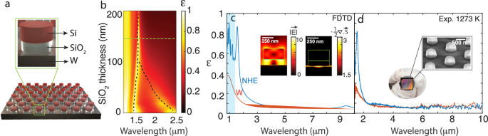
a Schematic showing the metasurface and structure of the individual resonator. b Calculated normal direction emissivity from NHE as a function of SiO2 thickness. The horizontal dotted green line represents the SiO2 thickness (140 nm) considered for the final design. c Calculated normal direction spectral emissivity of NHE (blue) and Tungsten (W) substrate (red). The wavelengths shaded in blue are beyond the range of our emissivity measurements. The inset shows the calculated cross-sectional electric field and divergence of the Poynting vector profile at the resonance (λ = 1.6 μm). d Measured emissivity curves near normal direction from NHE and W at 1273 K. The inset shows the optical and SEM images of fabricated NHE.
The weak coupling or high spacer thickness regime is particularly interesting for designing selective emitters as it enables spectrally selective and bright thermal emitters. Single-resonator designs suffer from a trade-off between the peak brightness and spectral selectivity27 that can be relaxed in the non-Hermitian design. The calculated (Fig. 2c) spectral emissivity curve (Fig. 2c) under weak coupling (SiO2 thickness = 140 nm) exhibits a sharp resonance peak at 1.6 μm. At this resonant wavelength, the magnitude of electric field distribution shows effective optical storage in the nearly lossless silicon resonator, while the divergence of the Poynting vector suggests that all thermal photons arise from the lossy plasmonic tungsten resonator (Fig. 2c, inset). This spatial decoupling of photon storage and thermal photon generation results in the relaxing of the trade-off between brightness and spectral selectivity of the NHE. Thus, the NHE operating in the weak coupling regime achieves the best of two worlds: high brightness from plasmonics and high spectral selectivity from dielectrics. Such emitters are promising for high-efficiency TPV systems.
Spectral efficiency characterization of NHE
We fabricated the NHE using standard planar nanofabrication processes (see materials and methods). We chose the SiO2 spacer thickness as 140 nm for a guaranteed operation in the weak coupling regime. The optical and SEM images of the fabricated metasurface are shown in the insets of Fig. 2d. The measured emissivity spectra at 1273 K demonstrate strong spectral selectivity resulting from resonantly enhancing emissivity at 1.6 μm and suppressing emission at longer wavelengths.
The thermal stability of selective emitter is crucial for practical TPV systems. We measured the temperature-dependent emissivity spectra of NHE held under vacuum (about 10−6 hPa) in the temperature range of 300–1273 K (Fig. 3a). The scanning electron microscope (SEM) images of NHE (insets of Fig. 3a) taken before and after cycling temperature through 1273 K showed minimal structural degradation. The resonance peak exhibited a temperature-dependent reversible redshift, which can be attributed to the temperature-dependent optical constants of the materials27. Using the measured emissivity curve at 1273 K, the emittance of NHE INHE at 1273 K was calculated (Fig. 3b). Strong suppression of thermal emission at longer wavelengths may be observed.
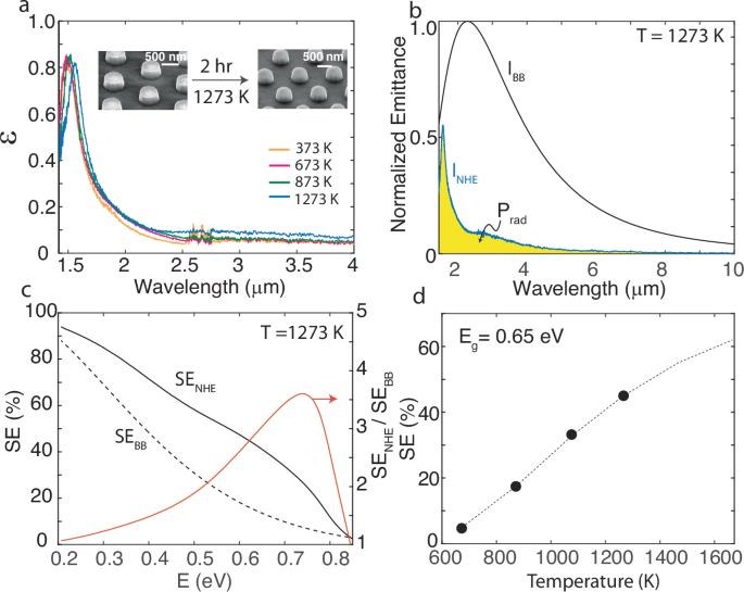
a Temperature-dependent emissivity from NHE shows minimal spectral degradation. The inset shows the SEM images of NHE before and after annealing at 1273 K under a high vacuum environment. b Calculated spectral emittance from NHE at 1273 K and a blackbody at the same temperature. Considering NHE as a Lambertian surface, total hemispherical power radiated from the unit surface area is given by the area under the emittance curve (shaded in yellow). c Spectral efficiency (left vertical axis) as a function of bandgap energy for NHE and blackbody at 1273 K. The SE enhancement of NHE over blackbody ((frac{S{E}_{NHE}}{S{E}_{BB}})) is plotted to the right vertical axis (red curve). d SE calculated at different temperatures considering a PV cell bandgap energy of 0.65 eV.
From the measured high-temperature emittance curves, the SEs of NHE and blackbody are calculated using Eq. (1). As evident from Eq. (1), SE is a function of Eg at any given T. Figure 3c plots the calculated SE of NHE and a blackbody emitter versus bandgap. Our NHE shows enhanced SE over that of a conventional blackbody emitter for a broad range of bandgap energies. The SE of NHE surpasses that of a blackbody emitter by over 300% when the bandgap is from 0.65–0.75 eV. If Eg = 0.65 eV, the SE of our NHE would increase monotonically with its operating temperature to reach 45% at 1273 K and 62% at 1673 K (Fig. 3d). This SE value is about the maximum possible for any metal-based emitter at the chosen operating temperature. An SE beyond these values can only be achieved by using a refractory metal with lower losses than that of tungsten26.
PV cell characterization and power conversion efficiency calculations
The overall heat-to-electricity conversion efficiency in a TPV module depends not only on the spectral efficiency of the emitter but also on the photovoltaic efficiency of the PV cell. Figure 4 shows the results of the characterization of a commercially available GaSb PV cell (JX Crystals Inc.). Given that the maximum SE enhancement of NHE over a blackbody happens in the bandgap range of 0.65–0.75 eV, a GaSb PV cell with an Eg of 0.72 eV is well-suited for our study. The external quantum efficiency (EQE) spectrum of the PV cell shown in Fig. 4a indicates a bandgap value of 0.708 eV (see the inset of Fig. 4a, and Materials and Methods section for details). The room temperature I–V characteristics of the cell under a 920 nm diffused laser illumination (0.35 W/cm2) are shown in Fig. 4b. The fill factor (FF), dark current density I0, and the open circuit voltage (VOC) were found to be 0.57, 10−4 A/cm2 and 0.36 V, respectively. If all photons emitted by our NHE were to be absorbed by the active area of this PV cell (100% collection), the total electrical power output (Pel) from the cell would be as plotted in Fig. 4c.
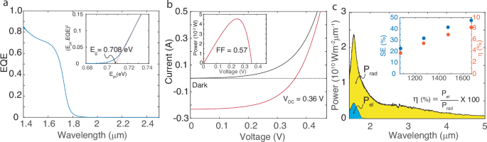
a The measured external quantum efficiency (EQE) spectrum of GaSb PV cell. The bandgap energy deduced from the EQE spectrum is shown in the inset b measured I–V curve and the output power (inset) with illumination (red curve) and without illumination (black). c Radiated power density from NHE (yellow) at 1273 K and electrical power density generated from GaSb cell (blue) is given by the area under the corresponding spectral power density curves. The inset shows temperature-dependent SE (blue circles) and η (red circles) values calculated using extracted cell parameters.
The power conversion efficiency ((scriptstyleeta =frac{{P}_{el}}{{P}_{rad}})) calculated using the temperature-dependent values for Prad (total radiated power) and Pel is plotted in the inset of Fig. 4c. Despite the high spectral efficiency of NHE, the overall conversion efficiency of the TPV system is significantly impacted by the poor performance of the GaSb PV cell. High dark current due to poor material quality and resistive losses within the cell and at the contacts lower the FF and VOC, resulting in smaller conversion efficiency. The best conversion efficiency expected with this PV cell is 5.4% at 1273 K.
To evaluate the practical power output performance of the NHE-GaSb pair at high temperatures, we built a basic working prototype of the TPV converter system. A large area (1.64 cm2) of NHE was fabricated using the planar fabrication process. The NHE was mounted on a cartridge heater with an integrated thermocouple (HeatWaveLabs) capable of heating up to 1200 K (Fig. 5a). A tungsten foil (0.2 mm thick) was placed on the heater head to block any radiation from the heater from reaching the active area of the cell. The GaSb PV cell with an active area (1.48 cm2) was placed close to the emitter (2 cm away). The entire setup was housed inside an ultrahigh-vacuum chamber. The measured I–V curves at different temperatures of the emitter are plotted in Fig. 5b. The magnitude of the reverse current is observed to increase with the emitter temperature. The dark current dramatically increases along with the photocurrent, suggesting that the PV cell suffers from substantial radiative heating32. The maximum power output, shown in Fig. 5c, from the complete TPV system reaches 10.8 mW at 1173 K. Considering the total emitted power from the emitter-tungsten foil assembly, our calculations suggest a TPV conversion efficiency η of 0.2%.
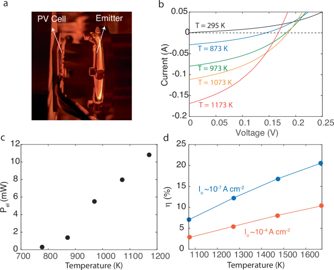
a An image of the NHE-GaSb TPV system operating at elevated emitter temperature (1173 K). b Measured I–V curves from the GaSb cell when the emitter is heated from 295 K to 1173 K. c Output electrical power generated for different emitter temperatures. d The η values were calculated at different temperatures using the extracted dark current value from PV-cell characterization (red) and theoretically predicted dark current value (blue).
Discussion
The poor efficiency observed here indicates that our TPV system is far from being optimum. Though we have demonstrated the best possible selective emitter, the PV cell and the setup need improvements. Optimizing the overall TPV system is the key to higher efficiencies16. Using less absorptive materials in the PV cell mount and cooling the PV cell could overcome the heating issue. The measured dark current density of the PV cell is about three orders of magnitude higher than the numbers reported in the literature16,33,34,35. This high dark current suggests that the material and methods of PV cell fabrication need refinements. High-quality GaSb PV cells could solve this problem. With these fixes implemented on our current TPV system, our NHE would result in overall TPV conversion efficiency, as shown by the blue line of Fig. 5d. Decreasing the dark current by a better quality PV cell is the key to nearly doubling the TPV efficiency to about 12% at 1273 K.
In conclusion, we demonstrated a hybrid metal-dielectric metasurface as a selective thermal emitter in a TPV system well-suited for harvesting mid-grade waste heat. The emitter, designed using the principles of non-Hermitian optics, employed coupled resonators to break the trade-off between spectral selectivity and peak brightness. This non-Hermitian emitter (NHE) surpassed the spectral efficiency limits set by conventional selective emitter designs and achieved 45% at 1273 K. This spectral efficiency is the highest possible for any metal-based thermal emitter at this temperature. Any further improvement requires better refractory plasmonic materials.
We also built and characterized a full TPV system using the NHE. The NHE operated at 1173 K in a vacuum, and the uncooled PV cell was a commercially available GaSb cell. The experimental results suggested significant radiative heating of the PV cell that reduced the TPV efficiency to less than 1%. Fixing this heating issue could boost the TPV efficiency to about 5%. Lowering the dark current of the GaSb PV cell by three orders of magnitude to its theoretical limit could boost the efficiency further to 12%.
Methods
Spectral efficiency calculation
To evaluate the SE of selective emitters reported in the literature (Fig. 1), we employed Eq. (1). Since different emitters are optimized to operate at different temperatures and bandgaps, we used the following procedure on all emitters to ensure fair comparison between them. We chose bandgap Eg as the photon energy, where the reported emissivity of the corresponding selective emitter drops to 0.25. Then, we selected the operating temperature T such that the peak of the blackbody power spectral density coincided with the wavelength at which the emissivity of the emitter crossed 50%. The emission bandwidth in the super-bandgap region ΔE was set to 0.15 eV for all emitters. The lower and upper limits of the integral to find the total radiated power were set to 0.05 eV and Eg + ΔE, respectively. The analysis in Fig. 1 is limited to selective emitters with measured high-temperature emissivity data available. When data were not available, especially for longer wavelengths, the lowest emissivity value was extended flat up to 0.05 eV.
Fabrication of the metasurface
The NHE samples were fabricated on a 0.5 mm thick tungsten substrate (MTI Corp.). Layers of SiO2 (140 nm), and Si (250 nm) were deposited on tungsten substrate using plasma-enhanced chemical vapor deposition (PlasmaTherm Versaline). A layer of e-beam resist (PMMA A4) was coated on the surface, and patterning was performed using standard e-beam lithography (Elionix ELS-G100). Next, an etch mask was deposited with 17 nm and 6 nm of Al2O3 and Cr, respectively, using an e-beam evaporator. Following a liftoff in acetone, the nanocylinders are formed using a reactive ion etch (Oxford, Plasmalab System 100/ICP 180) with a mixture of C4F8, SF6, CF4, and O2 at flow rates of 50, 5, 25, and 2 sccm, respectively. The capacitively- and inductively-coupled RF powers were maintained at 75 and 200 W, respectively.
Emissivity measurements
Reflectance (({mathcal{R}})) spectra of the metasurface were measured at elevated temperatures using a vacuum chamber with a heated stage (MicroOptik-MHCS1200) coupled to an FTIR microscope (ThermoFischer). A thermocouple (type S) was placed close to the metasurface (1 mm away) on the metallic stage, supporting the NHE to measure its temperature. A refractive objective (Edmund Optics) with a low numerical aperture of 0.08 was used to measure reflectance spectra. A polished gold surface with known reflectance values was used as the reference for reflectance measurements to obtain absolute values. Emissivity (equal to absorption) was calculated as (1-{mathcal{R}}).
PV cell characterization
Spectral responsivity, R(E), of the PV-cell was measured by performing Fourier Transform Photocurrent Spectroscopy (FTPS). EQE spectrum was obtained from the spectral responsivity as EQE(E) = (frac{R(E).E}{q}). I–V characterization of the cell was performed using a source measuring unit (Keithley 2450).
Simulation methods
Full-wave electromagnetic simulations were performed using a finite-difference-time-domain solver (Ansys Lumerical). Si and SiO2 optical constants at high temperatures were obtained by fitting measured reflectance and transmission of thin films with a Drude-Lorentz model for permittivity. Optical constants for tungsten were obtained by fitting measured reflectance curves with a Drude-Lorentz model. Simulations were performed under normal incidence plane-wave illumination.
Responses