Nonlinear quantum optics at a topological interface enabled by defect engineering

Introduction
The last two decades have seen the emergence of topological photonics as a new and powerful approach to the design of photonic devices with novel functionalities1,2,3,4,5,6,7. Many of these developments have been motivated by the fact that topological systems exhibit chiral or helical edge states that are confined to the boundary of the system and are remarkably robust against imperfections common to integrated photonic devices8,9,10. Examples of implementation of topological photonics in the linear regime include robust optical delay lines11, slow-light engineering12, waveguides, tapers, and re-configurable routers13,14,15,16,17,18. While early efforts in topological photonics focused on linear devices, more recent demonstrations have included nonlinear effects, extending the scope of possible applications to include lasers19,20,21,22, parametric amplifiers23,24, quantum light sources25,26,27,28 and frequency combs29. A more recent and intriguing direction has been exploring strong light-matter coupling to induce strong interaction between photons. To achieve this, microcavity exciton-polaritons30,31, transition metal dichalcogenides32 and quantum dots (QDs)33 were integrated into topological photonic devices. In particular, due to their scalability and high optical quality for on-chip single photon generation, there has been great interest in implementing QDs in topological photonic devices. For example, QDs have been utilised in various applications, such as internal light sources in topological photonic ring resonators34, topological 1D cavity lasers35, and topological slow-light waveguides36,37. They have also been used as integrated single-photon emitters for cavity-QED in topological nanocavities38,39, as well as for chiral quantum optics in fast and slow-light topological waveguides33,40,41, topological all-pass40,42 and add-drop filters43.
Efficient integration of several QDs in topological photonics could lead to the realisation of collective effects such as chiral super and sub-radiance effects and spin chains44. However, development in this direction has remained elusive due to several remaining challenges. By optimising solely around optical properties, we can inadvertently introduce challenges related to the environment of quantum emitters. Integrating QDs within stable environments is essential for high-performance single-photon emission and operation as few-photon nonlinearities. Achieving this in VH waveguides requires careful optimisation of the waveguide design, taking into account the stability of the environment of embedded quantum emitters. On one hand, position-dependence of the emitter’s coupling efficiency and chiral coupling in QD-coupled topological waveguides is a significant limitation in these quantum optics interfaces, as recently explored both theoretically and experimentally45,46. Moreover, regions of high directionality and high coupling efficiency are mostly present in the holes of the crystal rather than the material40,46,47, which is detrimental for coupling to solid-state quantum emitters.
Challenges associated with performing successful resonance fluorescence (RF) studies in conventional photonic devices have largely been addressed by embedding QDs in diode structures to minimise charge noise and reduce spectral wandering48,49,50,51,52. However, in photonic structures such as valley-Hall (VH) waveguides, extensive etching of the waveguide membrane exposes remaining sections to increased charge noise from surface charge traps, leading to higher spectral wandering and making stable charge state observation via RF particularly challenging53. These charge traps degrade QD performance if they are less than 40 nm away from these surfaces53,46, resulting in higher spectral wandering. No point within a typical VH-waveguide is more than 50-nm away from an etched surface. Given these considerations, it is unsurprising that topological structures with embedded emitters encounter difficulties in achieving RF and emitter-based strong nonlinear interactions, significantly hindering their potential for scalable quantum systems with high coherence and indistinguishability. Another remaining challenge is the efficiency of mode conversion at the topological-conventional waveguide interfaces40,43,54. Further optimisation of such mode conversion is essential for the efficient integration of these optical components for scalable photonic circuitry.
In this work, we report a novel platform based on the integration of QDs in lattice defects that overcomes many of the aforementioned challenges. To address these challenges, we remove specific etched holes within the un-modified topological waveguide (as illustrated in Fig. 1a(i–ii)) to create defect regions where QDs can be located without being in close proximity to etched surfaces. We focus on two types of defects, which we refer to as Mono and Tri-defects, involving the removal of one and three holes, respectively. The Mono-defect offers a minimal perturbation to the waveguide mode without leading to electric field localisation in the topologically non-trivial portion of the waveguide, thereby improving the QD environment while maintaining high transmission. The Tri-defect, on the other hand, is the smallest defect to produce a localisation within the topologically non-trivial region (a defect involving the removal of two holes produces a cavity mode only in the topologically trivial region), enhancing the Purcell factor for the QD. Figure 1e shows that the Mono-defect has little impact on the transmission through the topologically non-trivial spectral region of the waveguide’s operation. The Tri-defect offers a significantly greater simulated maximum Purcell enhancement in comparison to the Mono-defect, with the trade-off of a moderate decrease in transmission. While larger defects could be utilised, each with its own unique electric field localisation, coupling strengths and associated transmission loss, we have confined our study to these small defects, as larger defects lead to an increased mode volume, thus reducing the Purcell enhancement. Further optimisation of these defects, by introducing a tapering of the waveguide, or through manipulation of the size or position of the apertures around the defect, could lead to greater Purcell enhancements and reduced transmission loss, as has been demonstrated in conventional photonic crystal waveguide systems55,56,57. We believe that this method significantly reduces the adverse effects of charge instability caused by surface states and does not compromise the coupling efficiency of QDs into non-trivial topological modes. Such an approach promises to leverage the unique advantages of topological waveguides while circumventing the limitations imposed by conventional photonic crystal structures. We demonstrate that these defects can be utilised to achieve highly directional emission, and we harness the improvements to the QDs’ local environment to achieve the first demonstration of resonance spectroscopy and optical nonlinear response of quantum emitters at a topological edge state. Additionally, we use an inverse design approach to improve the mode conversion efficiency between topological and non-topological regions (see supplementary section S1), enhancing the scalability of the system.

a Schematic diagram of the (i) single aperture removed (Mono) defect waveguide and (ii) triple aperture removed (Tri) waveguide-coupled defect cavity. b An illustration of the perturbed unit cells that form the VH-waveguide and their bandstrutures, showing the formation of a band gap at the K point. c The C3 unit cell. d SEM image of the waveguide structure showing the location of the defect at point (1), scale bar represents 2 μm. e The frequency dependence of the transmission through the mono and tri defects presented on the left Y-axis (red) with the Purcell enhancement at the centre of the defects presented on the right Y-axis (Blue).
Results
Construction of a Valley-Hall waveguide with embedded quantum dots
The VH topological photonic crystal (PhC) used in this work is created from a honeycomb lattice of triangular holes in a semiconductor membrane. For these semiconductor-based QD systems, we grow a GaAs-based p-i-n diode using molecular beam epitaxy with InAs Stranski–Krastanov dots positioned in the middle of the intrinsic layer. This wafer design allows for fast tuning of embedded QDs via the quantum-confined Stark effect and reduces charge noise by modulating the electric field. The rhombic unit cell of the PhC contains a pair of triangular holes. Initially, with holes of equivalent diameters, the band structure of the PhC for TE polarisation shows a Dirac cone at the K point (and similarly at the ({K}^{{prime} }) point), as shown in Fig. 1b. By shrinking one triangle and expanding the other, a modified PhC supports a bandgap for TE polarised light. A notable aspect of the band structure is the opposite sign of the Berry curvature at the K and ({K}^{{prime} }) points, as demonstrated in ref. 58. By interfacing two of these perturbed photonic crystal structures together, one the inverse of the other, a topological waveguide interface can be created. The difference in Berry curvature at the connection of the two PhCs results in the confinement of counter-propagating edge states with opposing helicity at the interface58. The design used in this work utilises a small triangle side length of ({L}_{{rm{S}}}=0.7a/sqrt{3}) and a large triangle side length of ({L}_{{rm{L}}}=1.3a/sqrt{3}), which establishes a single-mode, topologically non-trivial, slow-light region within the waveguide59. In this work, we use a lattice constant of a = 265 nm.
Observation of high-directional contrast
A documented challenge for topological waveguides46,47 has been reliably creating highly directional emissions. Here, we demonstrate that the introduction of the Mono and Tri-defects are a way to create highly directional QD emission. Figure 2b(i–ii) show the Stokes S3 parameter, which for the un-modified waveguide and mono-defect characterises the degree of circular polarisation of the localised electric field. The strong light confinement in these structures locks the local polarisation of the light to its propagation direction. This interplay between polarisation and propagation direction leverages spin–orbit coupling, where the spin state associated with a particular transition of a quantum emitter determines its polarisation and, thus, its emission direction44. For the un-modified waveguide, regions of the waveguide that can achieve high directionality are located close to etched surfaces (<50 nm) from the waveguides apertures. Removing one of these apertures to form the mono-defect greatly increases the distance from the peak of the S3 value to any etched surfaces, and creates a better spatial overlap of the electric field intensity and the S3 map (see supplementary section S3). This distance is even greater for the Tri-defect. In the case of the Tri-defect, the mechanism for the directionality arises from an interference effect between the two cavity modes it supports55 with the wavelength dependence of the directionality shown in Fig. 2b(iii). More information on this mechanism for directional coupling within the Tri-defect cavity can be found in supplementary section S2.
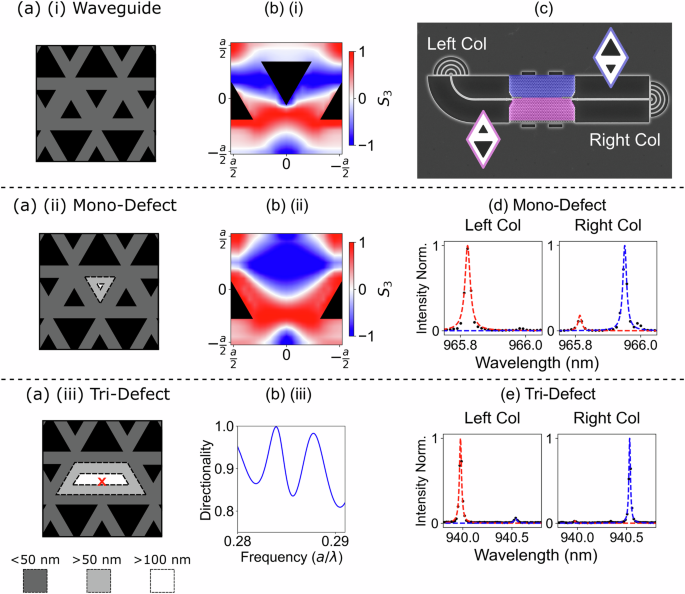
Within a(i–iii), regions less than 50 nm, greater than 50 nm and greater than 100 nm away from an etched surface are highlighted. b(i-ii) Shows the Stokes S3 parameter for the localised electric field at the centre of the slab waveguide slab for the (i) un-modified waveguide and (ii) the Mono-defect waveguide. b(iii) Shows the equivalent frequency dependence of the directionality of an emitter placed within the tri-defect cavity at the red cross indicated in (aiii). c SEM of the device showing the left and right collection ports (Col). d An example of high chiral contrast (85%) PL emission, from a QD located within the Mono-defect. e An example of high chiral contrast (92%) PL emission, from a QD located within the Tri-defect.
In order to demonstrate directional emission from QDs in these defect structures, μPL measurements of individual QDs were carried out, measuring from the left and right ports of the waveguide, as shown in the SEM of Fig. 2c. The resulting photoluminescence (PL) spectra from a single representative QD under a magnetic field in the Faraday geometry of 2T are illustrated in Fig. 2d, e for the mono-defect and tri-defect, respectively. These spectra reveal two Zeeman-split states, exhibiting an asymmetric intensity for the σ+ and σ− polarised transitions. Notably, the intensity asymmetry reverses when collecting PL from the opposite optical collection direction, indicating directional emission. The measured directional contrast for these two examples, reached a maximum of 85% for the Mono-defect and 92% for the Tri-defect, notably higher than the values achieved in our previous work with valley-Hall waveguides40,43. It is common to observe asymmetry in the contrast measured in either direction in experiments of this nature43,60, an effect that is visible in these results, and not yet fully understood.
Quasi-resonant and resonant excitation
To measure RF from a QD within the Tri-defect, we use the excitation scheme and device design illustrated in Fig. 3a. This consists of a VH-waveguide with a Tri-defect placed in the centre of the waveguide. The PhC is coupled via the inversely designed mode converter to two deep-etched Bragg grating couplers for far-field collection.
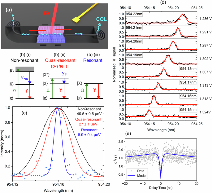
a Render of topological PhC with Tri-defect defect showing excitation scheme for resonant measurements. b(i) Energy level diagram illustrating non-resonant driving from the ground state (leftvert grightrangle) (at energy Ω) to above band state (leftvert Rrightrangle) and recombination to intermediate charge state (leftvert Xrightrangle) with non-resonant radiative emission energy γNR and back to ground state with resonant emission energy γ. (ii) Energy level diagram for the quasi-resonant scheme with P shell state (leftvert {X}^{* }rightrangle) (determined from the difference in pumping and emission wavelength Δλ = 14.83 nm) and intermediate emission γp to charge state (leftvert Xrightrangle). (iii) Energy level diagram for resonant scheme directly exciting charged excitonic state. c Comparison of linewidth in non-resonant, quasi-resonant, and resonant excitation showing a reduction in spectral wandering (Gaussian fit of linewidth given in top right corner). Non-resonant and quasi-resonant spectra are obtained via CCD spectrometer scans, while resonant spectra is obtained from bias-modulated photon-intensity with background subtraction (further details in supplementary section S6) while scanning laser with wavelengths shown on the x-axis in plot. d RF from a QD in a topological defect waveguide. RF signal obtained by scanning bias and measuring APD flux and normalised. Minimum linewidth observed was 8.9 ± 0.4 μeV at 954.16 nm. e Auto-correlation measurement of single dot emission under quasi-resonant excitation.
Figure 3b(i-iii) compares the energy level diagrams of non-resonant, quasi-resonant and resonant excitation schemes of a QD. In above-band excitation b(i), photons with energy greater than the bandgap of the QD material are used to create electron-hole pairs in the bulk material, which then relax through phonon emission and are captured by the quantum dot. The multiple steps and environmental interactions involved in this process lead to dephasing and broader emission linewidths compared to more targeted excitation methods. In quasi-resonant schemes b(ii), since the excitation energy is closer to the actual QD states, there are fewer relaxation steps involving phonons or other dephasing interactions, leading to a more coherent emission in comparison to the above band scheme61,62. Finally, moving to the resonant scheme b(iii), the excitation photons have precisely the energy needed to excite the QD directly from the ground state to an excited state. By directly pumping a single QD transition, we minimise the instability associated with that transition, leading to enhanced photon indistinguishably and coherence, and minimum time jitter63,64. This makes it desirable for deterministic single-photon generation, which is essential for large-scale quantum networks65. For the resonant measurements, the Tri-defect was excited from above with a resonant laser, scanning from 954.1 to 954.25 nm. The emission of the QD was modulated using an applied bias, to allow for the subtraction of the background laser scatter from the RF signal. To ensure a high signal-to-noise ratio, we introduced a cross-polarisation scheme that introduced a phase of π/2 between the linearly polarised pump laser and QD emission. A more detailed description of this process is discussed in the supplementary material S6. Figure 3c compares the non-resonant emission from a single QD excited with a 808-nm laser (red) with the equivalent quasi-resonant (P-shell, excited at 939.33 nm) and resonant scheme that delivers emission at 954.16 nm. Here a significant reduction in linewidth to 8.9 ± 0.4 μeV (resonant) from 40.5 ± 0.6 μeV (non-resonant) is observed, indicating a significant reduction in dephasing.
In Fig. 3d the normalised RF signal at different applied biases is shown. An RF peak from the emitter is present, and tunes 0.7 nm from 954.15 to 954.22 nm as the bias is changed. As illustrated in Fig. 3c, d, the absence of fine structure splitting in the emission spectrum suggests the QD is in a charged exciton state, either X− (negatively charged exciton) or X+ (positively charged exciton). We believe the ability to observe stable charged states can be attributable to the combined charge stabilisation/state tuning from the p-i-n diode structure and the minimised charge noise by having the QD in the Tri-defect region. Non-resonant and quasi-resonant excitation in and around the defect at low powers revealed very few emission lines, with the investigated QD line isolated from any others within the vicinity; this low dot density, and position-dependent excitation, helped ensure that the RF signal observed in our wavelength scans originate specifically from the QD located in the defect. In order to gauge the single photon behaviour, we performed a Hanbury Brown and Twiss (HBT) auto-correlation measurement under a quasi-resonant excitation giving us a second-order correlation function, g(2)(τ) (as a function of coincidence time delay τ). From Fig. 3e at zero time delay (τ = 0) we have observed strong anti bunching such that, g(2)(0) = 0.14 ± 0.05 showing we are operating in the single photon regime from a QD inside the Tri-defect region. More information on this measurement can be found in supplementary section S7.
Resonant transmission
By moving into a resonant transmission scheme (seen in Fig. 4a), the nonlinear response of the QD within the Tri-defect region can be investigated. A QD that is well coupled to an optical mode behaves non-linearly at the few-photon level. Single photons are reflected by the emitter, while multi-photon states are more likely to be transmitted. This occurs because the QD saturates after absorbing a single photon, making it transparent to additional photons arriving simultaneously. Consequently, the QD may act as a photon-number-dependent switch, enabling the manipulation of light at the quantum level for applications in quantum optics and information processing52,66. The observation of this phenomenon in this device indicates a strong interaction between the QD in the defect and photons in the topologically protected waveguide mode. Such phenomena underscore the potential of defect regions to enhance the interaction between photons mediated by topologically protected modes.
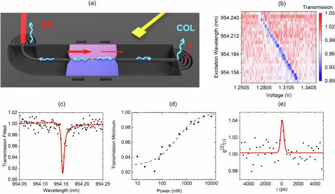
a Diagram showing resonant scattering in the tri-defect transmission. The Render shows the resonant transmission scheme, where the pump laser and far-field collection are at separate out-couplers.b Resonant transmission scan measured by sweeping voltage under a resonantly driven CW laser (at 50 nW). c An example of transmission spectra observed at 50 nW power at λL = 954.16 nm with a fitted maximum dip of 8% with a fano-lineshape. d Normalised transmission on resonance with the spectral line as a function of laser power, for λL = 954.16 nm. e Second-order auto-correlation function for photons transmitted through the topological waveguide and defect region at zero detuning. We observe clear bunching at τ = 0 (peaking at 1.038) using 200 ps bin width.
In the data presented in Fig. 4, continuous-wave pumping at resonant wavelengths and voltages are used to probe these nonlinear behaviours. At low excitation powers, on the order of 10 nW, the strongly attenuated guided laser light predominantly occupies zero and one photon states within a single QD emission cycle. When the wavelength of the incoming photons is resonant with the QD transition, the system exhibits a characteristic dip in the transmission spectrum, indicative of photon reflection by the QD. Figure 4b shows the waveguide transmission as a function of laser wavelength and applied voltage when the laser is tuned across the X± state of the QD. The consistent Stark tuning behaviour and matching linewidths of the RF emission and the transmission dip indicate that both measurements are associated with the same QD in the defect region. The transmission is normalised at each point to the transmission measured with the QD in an optically inactive state (at a bias of 1 V, in this case).
Figure 4c shows a snapshot of (b) with the excitation laser fixed at 954.16 nm, where it is possible to see the strongest transmission dip with a minimal Fano-lineshape (≈8% dip). The degree and width of the transmission dip allow us to model the cavity-waveguide coupling efficiency into the propagating modes. We can place a lower bound on this coupling from a fit to the transmission spectra for 50 nW (by taking an upper bound on the resonant decay rate as the measured quasi-resonant decay rate shown in supplementary section S5), giving a coupling efficiency of 61 ± 4% (details of calculation in supplementary section S9). In Fig. 4d, at an excitation wavelength of 954.16 nm, as we increase the input laser power we observe a transition towards higher photon occupancy within the laser field, which diminishes the transmission minimum via dot saturation (from ≈7% at 50 nW to ≈0.5% at 10 μW). The relationship between the transmission and the power is given by:
Where Pc is the critical power at which one photon within the time period of the QD’s lifetime, couples through the QD, and A is the minimum transmission dip. A least squares fit (represented by the dashed line) to the experimental data presented in Fig. 4d, gives A = 0.071 and Pc = 388 nW. This power-dependent transmission behaviour shows the nonlinear nature of the interaction.
By characterising the photon statistics of this nonlinear response, we can gauge the system’s ability to sustain the highly coherent interactions of the resonant scattering (operating in the coherent scattering regime using a pump power of 50 nW). In an ideal case, the QD will reflect single-photon components and only photon-photon bound pairs (multi-photon states) will transmit, leading to a bunching effect at τ = 0 in a g(2)(τ) measurement. In Fig. 4e, we can see a distinct bunching peak of g(2)(0) = 1.04 indicating the coherent scattering of single-photon components as predicted. This behaviour would be difficult to observe if not for a sufficiently high coupling efficiency from the cavity into the topological waveguide mode, and efficient collection of the light-by mode adaptors. This shows promise that these devices can become integrated into larger scalable systems.
Discussion
The successful demonstration of RF of QDs embedded within topological photonic crystal waveguides marks a notable advancement towards realising on-chip integrated quantum optical devices. The integration of QDs within defects provides enhanced stability and efficiency for single-photon sources, crucial for quantum computing, communication, and sensing technologies. The use of an inverse designed connection between the topological waveguide and conventional nanobeam structures significantly improves the coupling efficiency, facilitating better integration into larger photonic circuits. Additionally, the enhancement in chiral coupling within the defect-engineered regions enables precise control over the emission directionality of single photons, which is a critical factor for advanced quantum communication protocols. The exploration of nonlinear optical effects at the single-photon level within such topologically protected environments addresses a previously ongoing challenge in the field. The ability to manipulate single photons within these systems, as evidenced by the observed resonant/nonlinear behaviour under different excitation conditions, opens up new avenues for research and application. The engineered defect regions within photonic crystal waveguides, facilitating these interactions, underscore the potential of topological photonics in enhancing light-matter interactions at the quantum level.
Looking forward, coupling multiple QDs to the edge states67 within topological photonic systems presents an exciting direction for further research. By selecting appropriate defect sizes, for example using Tri-defects for strong emitter integration in small-scale devices and Mono-defects for minimising transmission losses in larger photonic networks, we can effectively manage free-space losses as the system scales up. The further the QDs are from the etched surfaces, the better their emission characteristics tend to be53, meaning that even within the defect regions, the emission efficiency and spectral stability of individual QDs can differ based on their exact distance from the etched surfaces. By exploring different defect geometries and optimisations, such as designing defects that shift the electric field intensity and chiral contrast maxima even further away from etched surfaces, we can mitigate the adverse effects of surface proximity. Additionally, surface passivation techniques68 can reduce losses due to scattering and absorption at the surfaces, enhancing the overall performance and scalability of the system. The collective dynamics between distant emitters69, within such a framework could unveil new quantum phenomena and enable the development of more complex and scalable quantum photonic circuits. The interplay between the quantum emitters and the topological modes, as facilitated by the engineered defects, offers a rich platform for exploring new regimes of light-matter interaction. This could lead to the realisation of novel quantum optical devices and functionalities, such as topologically protected quantum gates or routers, which are essential for the advancement of quantum information technologies.
Methods
Quantum dot wafer and device fabrication
In this work, the device layers were grown on a semi-insulating (100) GaAs substrate using molecular beam epitaxy. In order of deposition, the layers are: a 30-nm p-doped GaAs layer with a doping concentration of 2.0 × 1019 cm−3, a 25-nm p-doped GaAs layer with a doping concentration of 2.0 × 1018 cm−3, a 55-nm undoped GaAs layer to serve as a spacer, a 0.7-nm layer of InAs quantum dots formed via the Stranski–Krastanov growth method, another 55-nm undoped GaAs layer as a spacer above the quantum dots, a 30-nm n-doped GaAs layer with a doping concentration of 3.0 × 1018 cm−3, a 200-nm n-doped Al0.60Ga0.40As layer with a doping concentration of 3.0 × 1018 cm−3, a 950-nm undoped Al0.60Ga0.40As sacrificial layer, and finally, a 300-nm n-doped GaAs layer with a doping concentration of 3.0 × 1018 cm−3. This layer structure was designed to ensure robust electrical functionality while maintaining high optical quality in the quantum dot region. Nanophotonic devices were fabricated using standard lithography and wet/dry etching techniques. A 120-nm-thick SiOx hardmask was deposited using plasma-enhanced chemical vapour deposition, followed by the spin-coating of an electron beam-sensitive resist (CSAR). The device patterns were defined with 50kV electron beam lithography (Raith Voyager), then transferred into the hardmask and epitaxial layers using reactive ion etching (RIE) and inductively coupled plasma RIE, respectively. Finally, the hardmask and AlGaAs sacrificial layer were removed by a hydrofluoric acid wet etch.
Experimental methods
The sample was mounted in a superconducting magnet cryostat (CryoIndustries of America) operating at 4.2 K. The laser and QD emission, collected in the far-field scattering from out-couplers exhibit a primary polarisation along a specific linear axis. Taking advantage of this, the polarisation between the excitation and collection paths was modified using a series of linear polarisers, half-waveplates, and quarter-waveplates (or adjustable waveplates) to ensure a 90° difference in polarisation angle. This configuration (see supplementary Fig. S6) allows the scattered laser light to be rejected en route to the spectrometer or avalanche photodiode (APD). Additionally, voltage modulation was employed to filter out background fluctuations caused by electroluminescence or scattering processes from the pump laser during measurements and to compensate for changes in laser power resulting from tuning or instability.


Responses