Observation and enhancement of room temperature bilinear magnetoelectric resistance in sputtered topological semimetal Pt3Sn
Introduction
Improving charge-to-spin conversion efficiency has been an important research effort in spintronics ever since the discovery of spin-orbit torque1,2,3,4,5,6,7,8,9,10,11,12. Topological materials, including topological insulators5,6,7 and Dirac and Weyl semimetals8,9,10,11,12 (DSM and WSM), are proposed to have a large charge-to-spin conversion ratio due to the existence of surface or edge states and strong spin-orbit coupling. Large spin Hall angle and small switching current density have been reported in topological insulators at room temperature5,6, which shows great application potential in energy-efficient spin–orbit torque devices. Unlike topological insulators, though, bulk topological states exist in semimetals, where the conduction and valence bands are connected by nodes and lines in the bulk. The contribution of the bulk to conduction makes semimetals more favorable for industrial spin memory applications compared to topological insulator materials. Relatively large values of spin Hall angle have been reported in several WSM and DSM systems8,9,10,11,12.
Various methods are used to characterize the existence of topological states, with angle-resolved photoemission spectroscopy (ARPES) being the most commonly used one. ARPES gives direct evidence of the topological features, such as the Weyl nodes13,14,15, but requires a single crystal sample and in-situ measurement. Another approach is to use negative longitudinal magnetoresistance (NLMR) as evidence of topological states16,17,18,19,20,21, which may contain a variety of transport contributions19,20,21 and is not universal for all topological materials. Spin-momentum locking (SML)22,23,24,25, which fixes the spin direction of the electrons perpendicular to the momentum direction, is usually related to the existence of topological features, including the Dirac cone22,23 and Weyl nodes24, in the band structure, though it can be observed with trivial topology in Rashba bands25. Still, the existence of SML is a good indication of a potential existing topological state. However, direct detection of SML requires a non-local detection22, which necessitates a different device structure and fabrication method compared to other transport measurements such as spin–orbit torque (SOT) switching and magnetoresistance measurements. Moreover, since SML occurs along certain crystalline directions, direct detection of SML may not be suitable for polycrystalline materials. Recently, the discovery of bilinear magnetoelectric resistance (BMER) offers a straightforward means to demonstrate the existence of spin-momentum locking, consequently confirming the topological states26,27,28,29,30.
The illustration of BMER is shown in Fig. 1. With an electric field E applied to the sample, a second-order variation of the electron distribution occurs, which leads to a spin current that is proportional to E2,26, as shown in Fig. 1a. With a magnetic field applied, the population of the favored spin changes, which partially converts the spin current to a charge current, resulting in high and low resistance states, as shown in Fig. 1b, c. Existing in materials with topological spin texture, BMER changes linearly with both the magnetic and electrical fields without the presence of a magnetic layer. With a similar measurement setup to unidirectional spin Hall magnetoresistance (USMR)31,32,33,34,35 and unidirectional magnetoresistance (UMR)36, BMER can be measured with a simple two-terminal bar structure. This makes BMER a prospective candidate to indicate the existence of topological features in transport measurements. As topological behaviors may also exist in polycrystalline materials6, there is a potential that BMER may be observed. However, up to now, no such experiments have been carried out.
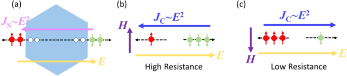
a The electric field E leads to a second-order change of the electron distribution, which results in a spin current proportional to E2. b, c With an applied magnetic field, electron populations of different spins change, which results in high and low resistance states.
Binary Pt–Sn alloys have been explored both theoretically and experimentally37,38,39,40 as a promising topological material. Different phases and compositions, such as PtSn4 and Pt3Sn, are proposed and demonstrated to have different topological properties37,38,39. With both topological surface states and bulk conduction, sputtered Pt3Sn was proved to show both topological states and type II Dirac semimetal features, with a large spin Hall angle as well as a robust NLMR39. Its small resistivity compared to other topological materials such as Bi2Se36, as well as the easy fabrication process by sputtering39, makes Pt3Sn an industrially compatible candidate for SOT-based technologies.
In this work, we report that the BMER value reaches 0.0034 nm2A−1Oe−1 in a sputtered type II semimetal Pt3Sn polycrystalline single layer at room temperature. Angular-dependent measurements at different directions have revealed unique BMER properties, which are related to the polycrystalline feature of the Pt3Sn material. Additionally, the magnitude of the BMER value is enhanced by ~2.35 times with an adjacent ferromagnetic CoFeB layer, which shows the potential for interfacial manipulation of the topological structures. The existence and manipulation of BMER in polycrystalline Pt3Sn film would pave the way for the design and characterization of the topological features in polycrystalline materials.
Results and discussion
The XRD results of a single layer of Pt3Sn (15 nm) (see methods for details of deposition) are shown in Fig. 2, where the inner image shows the pattern on the 2-D detector. Diffraction peaks for (111) and (002) Pt3Sn are present. The 2-D detector pattern contains two peaks which are, from left to right, the (111) and (002) diffraction peaks. The shape of the diffraction pattern is neither a ring (polycrystalline) nor a dot (single crystal) but a broadened line, suggesting textured growth of the Pt3Sn layer, and the intensity indicates the majority of crystals are ordered along the (111) direction. The crystalline structure of Pt3Sn along (111) and (002) is shown in the inner set of Fig. 2. With a space group of Pm–3m, the (111) direction of Pt3Sn has a 3-fold symmetry, which is favored for BMER observation26,28.
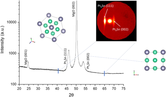
The inset shows the original 2D detector image in the range of 2θ containing the (111) and (002) Pt3Sn peaks. The inner set figures show the crystalline structure of Pt3Sn along (111) and (002), respectively, where the gray (green) atoms are Sn (Pt).
The single layer Pt3Sn (15 nm) film is then patterned into a 10 × 30 µm2 rectangular Hall bar for BMER measurements. An AC current with 2 mA amplitude and 133 Hz frequency is applied to the sample, and the second harmonic signal is measured along the longitudinal direction with an SR830 lock-in amplifier, as shown in Fig. 3a. An external field is applied with an angle θ with respect to the current direction in the XY plane. The measured angular-dependent signal under 30,000 Oe external magnetic field is shown in Fig. 3b. The field dependence and current dependence of the second harmonic voltage is shown in Fig. 3c, suggesting a linear relation with both the field and the current, which is characteristic of BMER. The BMER coefficient (chi) is defined with the following equation26,28:
where (triangle R) is the change of resistance and R is the resistance value, J is the current density and H is the applied magnetic field.
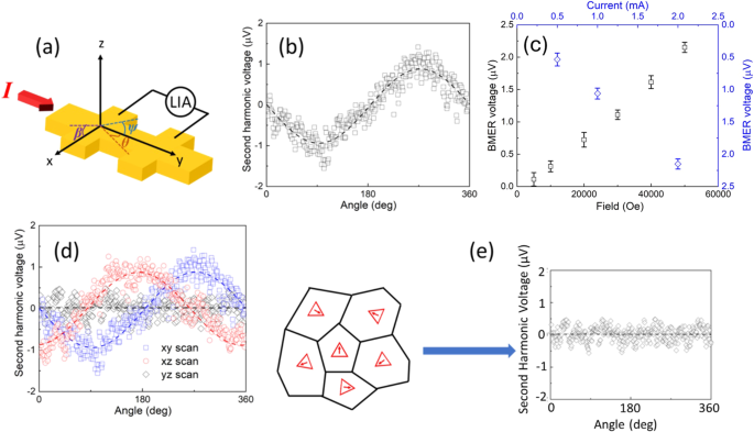
a Illustration of the second harmonic measurement and XY(θ), YZ(ψ), and XZ(β) scans. b Observed second harmonic voltage of XY scan. c Field dependence of second harmonic voltage shows the voltage is proportional to the applied field (black) and applied current (blue). d Second harmonic voltage for XY, YZ, and XZ scans, e Illustration of the absence of the z-direction signal in YZ and XZ scan. Crystallites in different directions contribute to z-direction signals which cancel with each other and result in a flat line in YZ scan.
With the contribution of the Nernst effect (NE) scaled by the Hall direction second harmonic measurement (see Supplementary Materials for details), the calculated BMER coefficient for Pt3Sn is 0.0034 nm2A−1Oe−1, which is comparable to previous research26,41. Pt3Sn has shown the existence of bulk topological states, as well as a charge-to-spin conversion ratio of up to 0.439. These features have contributed to a large BMER value, and the existence of BMER can, in turn, become the indicator of the existence of topological states and SML. In addition to the bulk topological states of Pt3Sn (111), the surface states of (002)-oriented grains may also have minor contributions to the BMER signals. Compared to characterization methods such as ARPES, using BMER for SML characterization may have other advantages besides its suitability for polycrystalline samples. The existence of BMER at different temperatures26,28 and a simple two-terminal measurement setup makes it suitable to be integrated into different transport measurement setups.
The BMER signal is also measured in XZ and YZ planes with β and ψ angular dependent measurements, as defined in Fig. 3a. Measurement results in the XZ plane show a similar trend and the same value of BMER compared to that in the XY plane. The BMER signal vanishes in the YZ plane, as shown in Fig. 3d. Compared to previous BMER research, the angular dependence of BMER values in XZ, YZ, and YZ planes are different in two aspects26,27,28: (1) BMER signal is absent in the YZ plane. (2) The XZ plane signal has the same angular dependence as the XY plane signal and is independent of the device pattering direction.
BMER exists in planes with threefold symmetry26,27,28. In previous BMER research in single crystals26,27,28, the signal in the XY plane stays the same regardless of the current direction with respect to the crystalline direction, the signal in the YZ plane has a 120° period for the current direction, and the signal in XZ plane is the difference of the signals in XY and YZ plane26,28. As shown in Fig. 2, the Pt3Sn layer is polycrystalline with most grains along 〈111〉 directions. The Pt3Sn grains have different in-plane textures, but the 〈111〉-textured grain has a 3-fold symmetric axis pointing toward z direction. In the XY plane, the grains lie randomly, as shown in Fig. 3e, and the direction with the largest positive BMER value is indicated as the triangles, as shown in Fig. 3e. As the Hall bar device contains multiple grains, each grain has a BMER contribution that differs in magnitude and direction. Contributions of the YZ plane from different grains with 〈111〉 texture cancel each other in the Hall bar device, which results in a zero net signal. Similarly, the crystalline direction dependence part in the XZ plane signal is also canceled, resulting in a net angular-dependent signal that is the same as the XY plane signal. The experimental observation of BMER in textured Pt3Sn demonstrates that BMER can exist in polycrystalline systems with isotropic values regardless of crystalline directions, which can provide strong evidence of the existence of SML in polycrystalline materials.
To further study this material system, two stack structures of Pt3Sn(10 nm)/Al(4 nm) (sample 1) and Pt3Sn(10 nm)/CoFeB(6 nm)/MgO(2 nm)/Al(4 nm) (sample 2) are deposited, and patterned into the same Hall bar structure as shown in Fig. 3a. The resistance values for the measured device on sample 1 and sample 2 are 730 Ω and 393 Ω, respectively. The two stack structures are measured under the same voltage (1.03 V), and the measurement current values for sample 1 and sample 2 are 1.4 mA and 2.6 mA, respectively. With the existence of the ferromagnetic layer, USMR and BMER should exist simultaneously in sample 2. Figure 4a shows the observed second harmonic signal for the structure at different field values in sample 2 (divided by 2.6 mA current), where both USMR + anomalous Nernst effect (ANE) & spin Seeback effect (SSE) contributions (green arrow, field-independent portion of the signal) and BMER + NE (orange arrow, field-dependent portion of the signal) are observed. The field dependence of the second harmonic signal is shown in Fig. 4b, where the intercept is the USMR and ANE&SSE contributions and the linear, field-dependent part is the BMER and NE contributions.
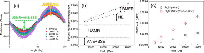
a Second harmonic resistance of sample 2 (Pt3Sn(10 nm)/CoFeB(6 nm)/capping layer), the applied current is 2.6 mA. b The field-dependent plot shows the contribution of ANE + SSE, USMR, BMER, and NE, respectively. c BMER ratio for Pt3Sn samples with and without an adjacent CoFeB layer. The adjacent CoFeB layer can increase the BMER value by a factor of 2.35.
To qualitatively study the BMER value, current shunting from the CoFeB layer needs to be considered. Another two samples with Pt3Sn(10 nm)/CoFeB(3,4.5 nm)/MgO(2 nm)/Al(4 nm) stacks are deposited and patterned together with sample 2 for resistivity measurement. The resistance is measured for this set of samples and fits with the parallel model: (frac{1}{{R}_{rm{total}}}=frac{wsigma }{l}{t}_{rm{CFB}}+frac{1}{{R}_{rm{PtSn}}}), where w(l) is the Hall channel width (length) and (sigma) is the conductivity of the CoFeB layer. The resulting resistance contribution for the Pt3Sn layer in sample 2 is 703 Ω, which is similar to the resistance of sample 1 (730 Ω). The resistance value is then used to calculate the current shunting in sample 2, and the current in layer Pt3Sn IPtSn = 1.46 mA is obtained. Since the value of IPtSn is similar to the applied current of sample 1, a direct comparison of ΔR/R in sample 1 and sample 2 can reveal the BMER coefficient difference in the Pt3Sn layer. Since the CoFeB contribution to the NE signal is negligible (see Supplementary Materials Fig. S2 for details), only the Pt3Sn layer can result in NE contribution. Thus the BMER values of Pt3Sn(10 nm) and Pt3Sn(10 nm)/CoFeB(5 nm) are scaled with the Hall direction second harmonic measurement of the Pt3Sn(10 nm) layer (see Supplementary Materials for details). The value ΔR/R versus the applied field is shown in Fig. 4c, indicating sample 2 has a BMER value ~2.35 times larger than sample 1. With the contribution of the Nernst effect removed (see Supplementary Materials for details), the BMER coefficient for sample 1 is 0.0040 nm2A−1Oe−1, which is similar to the coefficient (0.0034 nm2A−1Oe−1) in the Pt3Sn(15 nm) sample. With an adjacent CoFeB layer, the BMER coefficient changes to 0.0094 nm2A−1Oe−1. This result shows that adding a ferromagnetic layer can lead to an increase in the BMER value in the Pt3Sn layer.
The enhancement of BMER may have multiple origins. According to previous research, the value of BMER can be calculated by the following equation26:
where E is the electric field, l (w) is the length (width) of the device, λ is the hexagonal warping term26,42, and ({varepsilon }_{F})(vF) is the Fermi energy (Fermi velocity). Note that an out-of-plane term should also exist, but the textured polycrystalline feature of the Pt3Sn layer has canceled the contribution of the z dependence, as mentioned in the above discussion. Previous research has shown that an adjacent FM layer may open up a gap at the topological band structures43,44, which may account for the increase of the BMER value with an adjacent FM layer, as shown in Fig. 5. The Fermi level may not lie directly at the Dirac cone, and BMER or spin momentum locking can still exist regardless of the Fermi level location26,45. Without opening the gap, the Fermi velocity of the electrons near the Dirac point should be constant, as shown in Fig. 5a. Opening the gap will flatten the bottom part of the conduction band, which will reduce the Fermi velocity vF = (frac{{dE}}{hbar {dk}}), as shown in Fig. 5b. According to Eq. (2), the Fermi velocity has a power of 5. The topological features, such as the spin momentum locking, can still exist with a small gap opened46,47, but even a small change in Fermi velocity can result in a large change in BMER value. Both interface and bulk may have contributed to the BMER value change in Pt3Sn, as topological states may exist at both locations37,38,39.
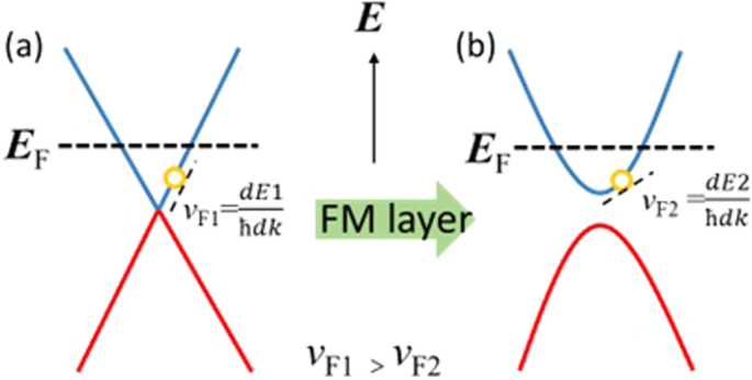
The original band structure is shown in a where the Fermi velocity is constant. The adjacent layer can open a gap at the Dirac cone as shown in (b), which will reduce the Fermi velocity of the electrons and, therefore, increase the BMER.
Recently, Shim et al reported the observation of UMR in antiferromagnetic materials48. The large effective magnetic field induced by antiferromagnetic spin canting was reported to enhance the distortion of the Fermi counter, which thus led to the enhancement of the existing field-dependent magnetoresistance signal (including BMER and the magnetoelectric resistance introduced by Rashba splitting49) and induced an observable UMR in antiferromagnetic/heavy metal bilayers. The enhancement of the magnetoresistance is induced by the strong spin canting effective field, which does not exist in ferromagnetic systems. Here, it is reasonable to speculate that the band opening for Pt3Sn could be introduced by the adjacent CoFeB layer as we observed the enhancement of BMER value in the Pt3Sn/CoFeB bilayer. Further study on this can be carried out in the future. For example, materials with an intrinsic small band gap can be selected to obtain a larger BMER value. The band structures of topological states can also be manipulated.
In conclusion, we observed BMER in sputtered Pt3Sn, which has both surface and bulk topological states. The BMER coefficient in a single 15 nm Pt3Sn layer can reach a value of 0.0034 nm2A−1Oe−1. The sputtered Pt3Sn has a textured polycrystalline structure, which results in the absence of out-of-plane BMER. With an adjacent CoFeB FM layer, the BMER value was enhanced from 0.0040 nm2A−1Oe−1 to 0.0094 nm2A−1Oe−1. We attributed the enhancement of BMER to the band opening induced by the FM layer, which results in a smaller Fermi velocity near the Dirac cone. The observation of the BMER enhancement paves the way for the manipulation of BMER value, and different contributions resulting in a higher BMER value can be further explored.
Methods
A single layer of Pt3Sn (15 nm) is deposited on a single-crystal MgO substrate with an eight-target sputtering system under base pressure 5 × 10⁻⁸ Torr. The sample was co-sputtered from targets of Pt and PtSn4 and the substrate was baked, deposited, and post-annealed for 1 h at 350 °C. A 4 nm Al layer is deposited on the top to protect the surface from oxidation. The Al capping layer is fully oxidized and, therefore, does not contribute to conduction. X-ray diffraction (XRD) measurements were then taken of the film in a Bruker D8 Discover diffractometer, utilizing a 2-D detector to observe the out-of-plane texturing and a Co-Kα1 source. Second harmonic measurements are operated with two SR830 lock-in amplifiers. The consistent background signal intrinsically from the lock-in amplifier is removed for better viewing.


Responses