Operando spin observation elucidating performance-improvement mechanisms during operation of Ruddlesden–Popper Sn-based perovskite solar cells

Introduction
Organic–inorganic hybrid perovskite solar cells (PSCs) are promising candidates for use as next-generation solar cells because of their cost effectiveness, high efficiency, flexibility, and wide scope of application, encompassing application to tandem solar cells. Since perovskites were used for the first time as solar cell absorber materials in 20091, efforts have been devoted to the development of various approaches to improve their efficiency, stability, and feasibility. These approaches include perovskite composition optimization2,3,4, development of carrier-transport materials5,6,7,8,9, and improvement of fabrication processes10,11. Their power conversion efficiency (PCE) has progressed rapidly. In fact, the highest efficiency has reached 26.1%12, which is comparable to that of state-of-the-art crystalline silicon solar cells. Nevertheless, the toxicity of Pb included in conventional Pb-based perovskites continues to pose an obstacle to the commercialization of PSCs. Therefore, lower-toxicity alternatives for Pb have been proposed, such as Sn, Ge, Bi, and Cu. Among them, Sn-based perovskites present great potential for providing high efficiency and stability because of their ideal optical band gaps and stable crystal phase13,14,15. However, Sn-based PSCs face the issue of the easy oxidation of Sn2+, which causes severe p-type doping of Sn-based perovskites, leading to low efficiency, poor stability, and reproducibility16,17,18. To suppress the Sn2+ oxidation in Sn-based PSCs, researchers have proposed various approaches including antioxidant introduction, solvent engineering, and device structure adjustment19,20,21,22,23,24. The PCEs of Sn-based PSCs, for which the typical device structure is presented in Fig. 1a, have exceeded 15%25 as a result of these studies, but they are still lower than those of Pb-based PSCs.

a Structure of a typical inverted PSC. b Film structures of 3D perovskite (left), RP perovskite (center), and 2D perovskite (right). c, d Chemical structures of spacer cations: BA+ (c) and PEA+ (d). e Schematic structure of the RP Sn-based PSC used for this study.
Introducing spacer cations (large organic cations) that form Ruddlesden–Popper (RP) Sn-based perovskites is a practical approach to improve the stability and efficiency of Sn-based PSCs. The introduction of such spacer cations will regulate the crystallization process, forming two-dimensional (2D) layered structures, which helps improve the thermal stability and hydrophobicity and suppress ion migration and self-doping of Sn-based perovskites26,27,28,29,30,31,32. The general formula for RP perovskites is expressed as A’2An−1BnX3n+3, where A’, A, B, and X respectively stand for spacer cations, small organic cations, metal cations, and halogen anions. When n → ∞, perovskite materials show a completely three-dimensional (3D) structure widely known as ABX3 (Fig. 1b, left). When n = 1, perovskite materials show a completely 2D structure, as shown in the right part of Fig. 1b. When 1 < n < ∞, perovskite materials show an RP phase with a layered structure (Fig. 1b, middle, n = 4). In 2017, Cao et al. reported RP Sn-based PSCs with butylammonium (BA+) spacer cations (Fig. 1c) for the first time. They exhibited a 2.5% PCE27. Liao et al. introduced 2-phenylethylammonium (PEA+) as spacer cations (Fig. 1d) and achieved a PCE of 5.94%26. Qiu et al. controlled the crystallization process using BA+ and PEA+ as mixed spacer cations, which suppress the formation of 2D intermediate phases31,32. Additionally, they introduced ionic liquid butylammonium acetate (BAAc) and succeeded in the fabrication of RP Sn-based PSCs, providing a PCE exceeding 10%31,32. Nevertheless, no report of the relevant literature describes charge states during device operation, although they are important for understanding RP Sn-based PSCs from a microscopic perspective.
Electron spin resonance (ESR) spectroscopy, a non-destructive, highly sensitive means of observing charge states inside samples at a molecular level, is regarded as a practical method to investigate the properties of electronic devices and their materials. We have applied ESR spectroscopy to organic electronic devices of various kinds33,34,35,36,37,38. As for PSCs, we have reported ESR spectroscopy studies mainly on Pb-based PSCs39,40,41,42,43. However, findings elucidating the charge states and their influence on the performance of Sn-based PSCs, especially of RP Sn-based PSCs, remain inadequate.
For this study, we use an operando ESR method to investigate the charge states and their effect on the device performance of RP Sn-based PSCs. First, we fabricated PSCs involving (BA0.5PEA0.5)2FA3Sn4I13 perovskites (where FA stands for formamidinium cations) and poly(3,4-ethylenedioxythiophene):poly(styrenesulfonate) (PEDOT:PSS) hole-transport layers (HTLs) and their thin-film samples. Then ESR measurements were taken in the dark and under illumination. As a result, hole diffusion from PEDOT:PSS layers to perovskite layers was observed by stacking these layers, forming an electron barrier at the PEDOT:PSS/(BA0.5PEA0.5)2FA3Sn4I13 interface. Moreover, electron transfer from perovskite to PEDOT:PSS was observed under illumination, which enhances the electron barrier at the interface. This enhanced electron barrier, which improves the passivation quality and carrier selectivity, contributes to the enhancement of RP Sn-based PSCs’ performance. These findings are of great importance for the further development of efficient and stable Sn-based PSCs.
Results and discussion
X-ray diffraction measurements of RP Sn-based perovskite
We confirmed the formation of RP Sn-based perovskites using X-ray diffraction (XRD) measurements (Supplementary Fig. 1). Diffraction peaks observed at 2θ ≈ 14.16° and 28.37° are consistent with those reported from earlier studies31,32. No other peaks were observed in the XRD pattern. These findings demonstrate the successful formation of (BA0.5PEA0.5)2FA3Sn4I13 RP Sn-based perovskites.
Device performance of RP Sn-based PSCs
This study used PSCs with a structure of indium tin oxide (ITO)/PEDOT:PSS/(BA0.5PEA0.5)2FA3Sn4I13/C60/bathocuproine (BCP)/Ag (Fig. 1e). Current density–voltage (J–V) characteristics and incident photon-to-electron conversion efficiencies (IPCEs) were measured on RP Sn-based PSCs fabricated on glass substrates with a dimension of 20 mm × 20 mm with active areas of 0.16 cm−2. The J–V curves and IPCE spectrum are presented respectively in Supplementary Fig 2a, b. The open-circuit voltage (VOC), short-circuit current density (JSC), fill factor (FF), and power conversion efficiency (PCE) were obtained, respectively as 0.45 V, 23.67 mA cm−2, 0.63, and 6.72%. The performances of RP Sn-based PSCs fabricated for this study are higher than those of 3D Sn-based PSCs reported in our earlier study44, which have similar device structures, and which are fabricated under similar conditions (Supplementary Table 2).
ESR spectra of thin-film samples under dark conditions
To investigate space-charge region formation at the PEDOT:PSS/(BA0.5PEA0.5)2FA3Sn4I13 interface by stacking these layers, ESR measurements were taken of thin-film samples of three kinds: pristine PEDOT:PSS films (Fig. 2a), PEDOT:PSS films treated using the solvent of perovskite precursor (treated-PEDOT:PSS, Fig. 2b), and the stacked samples of PEDOT:PSS/(BA0.5PEA0.5)2FA3Sn4I13 (Fig. 2c). For convenience, we designate the spin-coating of perovskite layers on PEDOT:PSS herein as the “stacking process”. The treated-PEDOT:PSS films and the PEDOT:PSS/(BA0.5PEA0.5)2FA3Sn4I13 stacks can be regarded as having identical properties to those in complete cells. By contrast, the pristine PEDOT:PSS films have properties that are unlike those in complete cells.

a–c Schematic structures of PEDOT:PSS thin films (a), treated-PEDOT:PSS thin film (b), and PEDOT:PSS/(BA0.5PEA0.5)2FA3Sn4I13 stacked film (c). d ESR spectra of thin-film samples in the dark. e, f Chemical structures and spin states of a PEDOT polaron (e) and a PEDOT bipolaron (f). g, h Schematics of electron barrier formation mechanisms at the PEDOT:PSS/(BA0.5PEA0.5)2FA3Sn4I13 interface by stacking these layers: initial state at the PEDOT:PSS/(BA0.5PEA0.5)2FA3Sn4I13 interface, holes diffuse from the PEDOT:PSS layer to the perovskite layer driven by a difference in the Fermi levels (g); and an electron barrier forms at the PEDOT:PSS/perovskite interface (h). In this figure, VL, CBM, VBM, and EF, respectively represent the vacuum level, the conduction band minimum, the valence band maximum, and the Fermi level.
Figure 2d presents ESR spectra of thin-film samples at room temperature (approx. 300 K) in the dark. From the pristine PEDOT:PSS film, an ESR signal with a g-factor, g, of 2.0030 ± 0.0001, and a peak-to-peak linewidth, ΔHpp, of 0.53 ± 0.01 mT was observed. The g-factor is consistent with reported g-factors of positive PEDOT polarons40,43. By contrast, the treated-PEDOT:PSS film shows an ESR signal with g = 2.0030 ± 0.0001 and ΔHpp = 0.67 ± 0.01 mT. It is particularly interesting that the peak-to-peak ESR signal intensity decreases considerably compared to pristine PEDOT:PSS films. This observation can be ascribed to the fact that the solvent treatment changes the morphology of PEDOT:PSS films, converting some ESR-active polarons (Fig. 2e) to spinless bipolarons (Fig. 2f). This finding is consistent with earlier results showing that a solvent with a strong polarity such as ethylene glycol and dimethylsulfoxide (DMSO) changes the PEDOT:PSS film morphology45,46, converting polarons to bipolarons and reducing the ESR intensity43,47. The same phenomenon occurred in the solvent treatment in this study using a mixture of dimethylformamide (DMF) and DMSO. An ESR signal with g = 2.0029 ± 0.0001 and ΔHpp = 0.49 ± 0.01 mT is observed from PEDOT:PSS/(BA0.5PEA0.5)2FA3Sn4I13 stacks. The signal intensity is higher compared with that of the treated-PEDOT:PSS film, which suggests that some bipolarons are converted to polarons by stacking. In other words, holes diffuse from PEDOT:PSS to (BA0.5PEA0.5)2FA3Sn4I13, which causes the de-doping of PEDOT. It should be described that the ESR signals derived from perovskite layers cannot be observed because of their Pauli paramagnetism nature, resulting in low ESR intensity, and because of the heavy-atom effects of Pb or Sn, leading to short spin-lattice relaxation time and broad ESR linewidths39,40,41,42,43,44,48.
The hole diffusion from PEDOT:PSS to (BA0.5PEA0.5)2FA3Sn4I13 is driven by a difference in the Fermi levels, EFs, in the stacking process (Fig. 2g and Supplementary Fig. 3a). Some bipolarons convert into polarons, which raises the signal intensity. As a result of the hole diffusion, an electron barrier forms at the PEDOT:PSS/(BA0.5PEA0.5)2FA3Sn4I13 interfaces (Fig. 2h and Supplementary Fig. 3b). Thereby, the field-effect passivation is enhanced (Fig. 2h). This enhanced passivation decreases the minority carrier concentration in the (BA0.5PEA0.5)2FA3Sn4I13 layer near the PEDOT:PSS layer, which reduces interface recombination.
During our earlier study, hole diffusion from PEDOT:PSS layers to perovskite layers was observed during the stacking process in Pb-based PSCs43. In contrast, hole diffusion from perovskite to PEDOT:PSS was observed in PEDOT:PSS/3D Sn-based perovskite (FA0.75MA0.25SnI3 and FA0.75MA0.25(I0.75Br0.25)3) (where MA stands for methylammonium cations) during the stacking process44,48. This diffusion is reportedly attributable to the oxidation of Sn2+, which deepens the EF of the perovskite layers (Supplementary Fig. 3c–e). This difference in the hole diffusion direction between perovskites and PEDOT:PSS suggests that the EF of RP Sn-based perovskites is shallower than that of 3D Sn-based perovskites. Although accurate measurement of the EF of Sn-based perovskites is challenging because of the susceptibility of Sn2+ to oxidation, the relative relation between the EFs was clarified through the charge diffusion observed via ESR measurements, which indicate that RP Sn-based perovskites are oxidized only slightly, demonstrating superior stability against oxidation compared to 3D Sn-based perovskites.
Operando ESR under open-circuit conditions
Operando ESR measurements were taken of RP Sn-based PSCs to investigate interface carrier diffusion under the open-circuit condition. Figure 3a shows the ESR spectra of an RP Sn-based PSC under one-sun illumination under open-circuit conditions. ESR signals of PEDOT polarons with g = 2.0028 ± 0.0001 and ΔHpp = 0.44 ± 0.01 mT were observed, similarly as for the PEDOT:PSS/(BA0.5PEA0.5)2FA3Sn4I13 stacked sample. Under illumination, the g-factor and peak-to-peak signal intensity remain almost identical, whereas the ESR line shape changes and the ESR linewidth increases considerably. Because no clear change was observed in the ESR spectrum of treated-PEDOT:PSS films under illumination (Supplementary Fig. 4), these changes can be attributable to the electron injection from (BA0.5PEA0.5)2FA3Sn4I13 to PEDOT:PSS. The number of spins, Nspin, of PEDOT polarons is depicted in Fig. 3b together with VOC. The Nspin increases from 5.1 × 10¹³ to 1.4 × 10¹⁴ after 19.5 h of illumination. It decreases slightly to 1.3 × 10¹⁴ after the subsequent dark storage for 9.5 h. The normalized VOC(t), VOC(t)/VOC(0), increases by approximately 40% after illumination for 20 h (Fig. 3b). As depicted in Fig. 3b, the correlation between an improvement in VOC and an increase in Nspin is apparent. Details of its origin are discussed later herein. J–V performances measured before and after 20 h illumination are summarized in Supplementary Fig. 5a and Supplementary Table 1.
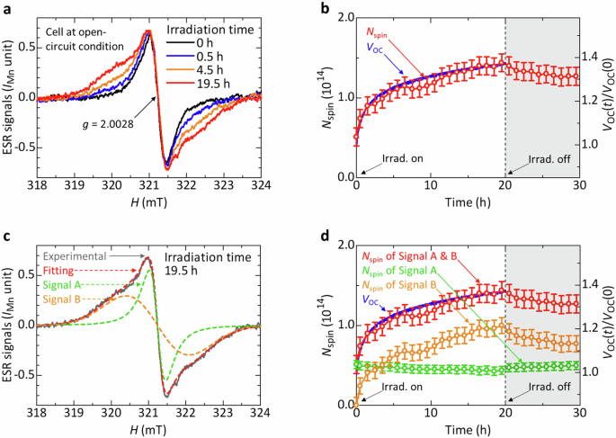
a ESR spectra of the RP Sn-based PSC. b Transient responses of the Nspin and VOC. c Fitting analysis of an ESR spectrum obtained after 19.5 h illumination. d Transient responses of the Nspin of PEDOT polarons and the VOC. Here, the Nspin of PEDOT polarons comprises Nspin of Signal A (mobile polarons) and Nspin of Signal B (localized polarons).
To analyze the change of charge states under illumination, we analyzed ESR spectra using a least-squares method with Igor Pro (ver. 6.36). Lorentzian and Gaussian formulas are used to describe the ESR spectra of semiconductor materials, where Lorentzian formulas originate from spins of mobile charges and Gaussian formulas originate from spins of localized or trapped charges. The fitting formulas used for this study are
where subscripts L and G respectively denote the quantities for Lorentzian and Gaussian functions, H represents the magnetic field, I(H), IL,j(H), and IG,k(H) represent the integrated absorption intensities, H0,L,j and H0,G,k represent the resonance magnetic fields, wL,j and wG,k are related to the half widths at half maximum of the absorption intensities, and hL,j and hG,k represent the absorption intensities. The g-factor and ΔHpp are obtainable using the following equations (Eqs. 4–6) as
where v and μB, respectively represent the resonance frequency and the Bohr magneton.
The fitting analysis of ESR spectra indicates that the ESR spectra comprise a narrow Lorentzian formula (Signal A) and a broad Gaussian formula (Signal B) (Fig. 3c). In the dark, the spectrum can be fitted successfully to a Lorentzian signal (Signal A) with g = 2.0028 ± 0.0001 and ΔHpp = 0.44 ± 0.01 mT, which is derived from mobile polarons in PEDOT. Under illumination, a Gaussian signal (Signal B) with g = 2.0028 ± 0.0001 and ΔHpp = 1.69 ± 0.01 mT appears. The broad linewidth suggests low mobility of polarons, indicating that Signal B is derived from localized PEDOT polarons. Figure 3d presents the transient response characteristics of Nspin and VOC. The Nspin of Signal A decreases from 5.1 × 10¹³ to 4.3 × 10¹³ after 19.5-h illumination and increases to 5.0 × 10¹³ after subsequent storage in the dark for 9.5 h. The decreased Nspin of Signal A can be ascribed to the de-trapping of electrons at PEDOT polarons, which converts them into bipolarons. In contrast, Gaussian signals are not observed in the dark but appear under illumination. The Nspin of Signal B increases from 0 to 1.0 × 10¹⁴ after 19.5 h irradiation and decreases to 7.7 × 10¹³ after subsequent 9.5-h dark storage. The increased Nspin of Signal B suggests that some electrons diffuse from (BA0.5PEA0.5)2FA3Sn4I13 to PEDOT:PSS under illumination. These electrons are trapped by bipolarons and leave localized, relatively immobile polarons, which are possibly located near the PEDOT:PSS/(BA0.5PEA0.5)2FA3Sn4I13 interface. The absolute value of the variation of the Nspin under illumination, ΔNspin, for Signal A (0.8 × 10¹³) is one order of magnitude smaller than that for Signal B (1.0 × 10¹⁴). Therefore, the change in Signal B mainly contributes to the total Nspin. Signal B might therefore have a strong effect on VOC improvement. From this finding, we surmise that the electron diffusion from (BA0.5PEA0.5)2FA3Sn4I13 to PEDOT:PSS under illumination contributes to the VOC improvement of RP Sn-based PSCs.
The charge transfer mechanism at the PEDOT:PSS/(BA0.5PEA0.5)2FA3Sn4I13 is explained hereinafter (Fig. 4). Hole diffusion from (BA0.5PEA0.5)2FA3Sn4I13 to PEDOT:PSS occurs under illumination, which increases the hole density in PEDOT:PSS and which converts some mobile polarons into bipolarons, leading to a decrease in Nspin of Signal A. This elemental process weakens the upward band bending at the interface (Fig. 4a). However, electrons injected from (BA0.5PEA0.5)2FA3Sn4I13 to PEDOT:PSS recombine with bipolarons and form localized polarons near the PEDOT:PSS/(BA0.5PEA0.5)2FA3Sn4I13 interface, which results in an increased Nspin of Signal B. Thereby, the band bending at the interface is enhanced (Fig. 4b). The electron injection to PEDOT:PSS (the increase of Nspin of Signal B) is dominant. Therefore, the electron barrier at the interface is eventually enhanced under illumination. This band-bending enhancement causes enhanced field-effect passivation (Fig. 4c), leading to improvement in VOC.

a Hole diffusion from the perovskite layer to the PEDOT:PSS layer under illumination and resulting electron barrier reduction. b Electron diffusion from the perovskite layer to the PEDOT:PSS layer and resulting enhanced electron barrier. c Enhanced electron barrier at the PEDOT:PSS/perovskite interface as a result of the two elemental processes. In this figure, CBM and VBM, respectively, represent the conduction band minimum and the valence band maximum.
Effects of ultraviolet light and consideration of electron injection mechanism
To clarify the mechanism of electron injection from (BA0.5PEA0.5)2FA3Sn4I13 to PEDOT:PSS in RP Sn-based PSCs under illumination, an ultraviolet (UV) filter that cuts light with wavelengths shorter than 420 nm was used to clarify UV light effects on the device performance and charge behavior. For clarity, periods in operando ESR measurements are divided into some regions designated by i–ix (Fig. 5a, b). We first took a measurement on an aged solar cell that had experienced the operando ESR measurement described above, which had been stored in the dark for about 300 days in an N2 atmosphere (Fig. 5a). This measurement consisted of illumination four times (i, iii, v, vi), separated by dark storage two times (ii, iv). For the first 20 h of the third irradiation (v), a UV filter was used to remove UV light from the incident light. Results show that the normalized VOC of the device remained at about 1.3 after 300 days of storage, which reflects the excellent stability of the RP Sn-based PSCs used for this study. Moreover, it is noteworthy that the non-zero Nspin of Signal B in the aged cell suggests markedly slow relaxation of localized PEDOT polaron. This slow relaxation is evidence that Signal B originates from long-lifetime, trapped polarons in PEDOT:PSS.

a Transient responses of the aged PSC, which had been stored for about 300 days in N2 atmosphere, under illumination with and without UV components. b Transient responses of the fresh PSC under illumination with and without UV components. Notations i–ix represent different periods of the operando ESR measurements under different illumination conditions. c, d Schematic diagrams of electron injection to PEDOT:PSS: hot electrons are generated by absorbing short-wavelength photons and are injected from perovskite to PEDOT:PSS (c). The electron barrier at the interface is enhanced (d). In panels c, d, CBM and VBM respectively represent the conduction band minimum and the valence band maximum.
As presented in Fig. 5a, the Nspin of Signal A is almost constant compared to that of Signal B, but it slightly decreases under illumination (i, iii, v, vi) and increases in the dark (ii, iv). Additionally, for Signal A, no clear effect of UV light is found. In contrast, behaviors of the Nspin of Signal B and the VOC change depending on the presence and absence of the UV component. The Nspin of Signal B increases under illumination with UV (i, iii) and decreases in the dark (ii, iv). However, under illumination without UV (v), the Nspin of Signal B does not increase but instead decreases continuously from the preceding dark condition. After removing the UV filter (vi), it increases again and exhibits the same behavior with the first and second illumination (i, iii). The VOC increased under illumination with UV and subsequently remained almost constant. Under illumination without UV (v), however, the VOC increases first but subsequently decreases slightly during illumination. After removing the UV filter (vi), the VOC is regenerated to the same level with the second irradiation with UV and keeps constant value for a remaining time. This result indicates that UV light participates in the electron injection process and in the enhancement of the electron barrier.
We further took operando ESR measurements of a fresh cell. In this case, the solar cell experienced, in order, illumination for 20 h without UV (vii), illumination for 20 h with UV (viii), and illumination for 20 h without UV (ix) (Fig. 5b). Results similar to those of the aged cell were observed. The Nspin of Signal A decreases monotonically under irradiation, whereas the Nspin of Signal B and VOC shows different behaviors under illumination with and without UV. The Nspin of Signal B and the normalized VOC respectively increase to 1.3 × 10¹³ and 1.07 during the first illumination without UV (vii), and respectively increase further to 6.4 × 10¹³ and 1.08 after removing the UV filter (viii). After inserting the UV filter again at 40 h (ix), the Nspin and normalized VOC are reduced respectively to 4.8 × 10¹³ and 1.07, and subsequently remain almost constant. These results suggest that hot electrons excited by high-energy photons participate in the electron injection to PEDOT:PSS layers.
Measurements taken for this study also revealed that the increase in VOC under the first illumination without UV (vii) was greater than that under illumination with UV (viii), although the increases in the Nspin of Signal B showed the opposite relation. The origin of this phenomenon is inferred as follows. Under the first illumination, injected electrons are trapped near the PEDOT:PSS/(BA0.5PEA0.5)2FA3Sn4I13 interface, which contributes strongly to the electron-barrier enhancement and the VOC improvement. In contrast, the subsequently injected electrons are trapped more distant from the interface, exerting a smaller effect on the electron-barrier enhancement and the resulting VOC improvement.
The possibility exists that carriers in the PEDOT:PSS layer might be excited by UV and subsequently transferred to the (BA0.5PEA0.5)2FA3Sn4I13 layer. However, the absorbance of PEDOT:PSS is considerably lower than that of perovskite layers. Also, the ESR signal of treated-PEDOT:PSS remained unchanged under one-sun illumination (Supplementary Fig. 3). These findings suggest that only a few excess carriers are generated in PEDOT:PSS under illumination. Therefore, carrier transfer from PEDOT:PSS to perovskite layers is regarded as a minor process at the PEDOT:PSS/(BA0.5PEA0.5)2FA3Sn4I13 interface.
Operando ESR under short-circuit conditions
ESR measurements under short-circuit conditions were also performed. Figure 6a shows the ESR spectra of a fresh cell under short-circuit conditions. Results similar to those obtained under open-circuit conditions were observed. The g-factor (g = 2.0028 ± 0.0001) and ESR intensity remain almost identical during illumination, whereas the ESR linewidth increases (Fig. 6a). We conducted a fitting analysis of these spectra. As depicted in Fig. 6b, they can be fitted to a Lorentzian signal (Signal A) with g = 2.0028 ± 0.0001 and ΔHpp = 0.51 ± 0.01 mT derived from mobile PEDOT polarons and a Gaussian signal (Signal B) with g = 2.0028 ± 0.0001 and ΔHpp = 1.99 ± 0.01 mT derived from localized PEDOT polarons. Figure 6c presents the transient responses of the Nspin and normalized JSC. Under illumination, the Nspin of Signal A decreases slightly from 6.0 × 10¹³ to 5.4 × 10¹³, whereas the Nspin of Signal B increases from 0 to 6.4 × 10¹³. Some correlation exists between the increase of Nspin and the improvement of JSC. This correlation is similar to that observed under open-circuit conditions. We hypothesize that, similarly to the case under open-circuit conditions, the JSC improvement is attributable to electron diffusion from (BA0.5PEA0.5)2FA3Sn4I13 to PEDOT:PSS under illumination and to the resulting improved field-effect passivation. J–V performances measured before and after 20-h illumination are summarized in Supplementary Fig. 5b and Supplementary Table 1. Similar performance improvements were also confirmed for 20 mm × 20 mm solar cell devices by repeated V scans under continuous illumination (Supplementary Fig. 6). The JSC, VOC, and FF increased under illumination, leading to the improvement of PCE.

a ESR spectra of the RP Sn-based PSC under illumination. b Fitting analysis of an ESR spectrum obtained after 19.5 h illumination. c Transient responses of the Nspin of PEDOT polarons and the JSC. Here, the Nspin of PEDOT polarons comprises Nspin of Signal A (mobile polarons) and Nspin of Signal B (localized polarons).
Conclusions
As described herein, we investigated performance-improvement mechanisms in RP Sn-based PSCs by taking ESR measurements of thin-film test samples and solar cells. Hole diffusion from PEDOT:PSS to (BA0.5PEA0.5)2FA3Sn4I13 occurs because EF difference was observed by stacking these layers, thereby forming an electron barrier at the PEDOT:PSS/(BA0.5PEA0.5)2FA3Sn4I13 interface. This finding suggests a shallow EF of RP Sn-based perovskite compared with conventional 3D Sn-based perovskites, demonstrating excellent stability against oxidation. Additionally, results indicate that, under illumination, hot electrons generated by short-wavelength light are further injected from (BA0.5PEA0.5)2FA3Sn4I13 to PEDOT:PSS, thereby enhancing the electron barrier at the interface. The improved field-effect passivation causes VOC and JSC improvement in the performance of RP Sn-based PSCs during device operation. The findings of this ESR study enhance the understanding of the properties of buried interfaces of Sn-based PSCs considerably and demonstrate the applicability and potential of ESR spectroscopy for characterizing field-effect passivation properties at the HTL–perovskite interface. Furthermore, using operando ESR spectroscopy, changes in field-effect passivation properties and their causes can be monitored during device operation. This approach can be applied effectively to Sn-based PSCs of various types, allowing for the comprehensive evaluation of their passivation properties at the buried HLT–perovskite interfaces. Accumulating data of various kinds of Sn-based PSCs might ultimately contribute to the development of strategies for improving Sn-based PSC performance.
Experiment methods
Preparation of perovskite precursor solutions
After butylamine hydroiodide (B4433, >97.0%; Tokyo Chemical Industry Co., Ltd.), 2-phenylethylamine hydrochloride (P6513, >98%; Sigma-Aldrich Corp.), formamidine hydroiodide (F0974, >98.0%; Tokyo Chemical Industry Co., Ltd.), tin(II) iodide (T3449, >97.0%; Tokyo Chemical Industry Co., Ltd.) and tin(II) fluoride (334626, 99%; Sigma-Aldrich Corp.) were weighed to a molar ratio of 1:1:3:4:0.6, 5-wt% guanidine hydroiodide (G0450, >97.0%; Tokyo Chemical Industry Co., Ltd.) was added. A solvent with a volume ratio of dimethylformamide (DMF) (040-32815, ≥99.0%; Fujifilm Wako Pure Chemical Corp.):dimethylsulfoxide (DMSO) (042-02926, ≥99.0%; Fujifilm Wako Pure Chemical Corp.) = 4:1 was added with a concentration of the solution to be 250 mg ml−1. After the solution was stirred at 550 rpm at 70 °C for at least 12 h in the dark, it was passed through a filter (0.45 μm, RephiQuik Syringe Filter RJF1345NH PTFE; Rephile Bioscience Ltd.) before use.
Device and test sample fabrication
The PSC structure fabricated for this study is presented in Fig. 1e. For ESR measurements, 20 mm × 3 mm quartz substrates coated with 150-nm-thick ITO were used. The substrates were cleaned ultrasonically in isopropyl alcohol (IPA) (29112-63, ≥99.0%; Nacalai Tesque, Inc.) for 5 min with subsequent ultrasonic cleaning in acetone (00309-93, ≥99.0%; Nacalai Tesque, Inc.) for 5 min. After this cleaning process was repeated three times, the substrates were dried with a nitrogen gun. The PEDOT:PSS (CleviosTM P VP AI 4083) aqueous dispersion was passed through a filter (PVDF, 0.45 μm, GD/X Syringe Filter 6872-1304; Whatman plc.), then spin-coated onto the substrates at 1000 rpm for 10 s, and subsequently at 4000 rpm for 60 s. The substrates were annealed at 140 °C for 20 min. The samples were transferred into a nitrogen-filled glove box with an oxygen concentration of approx. 0.5 ppm and H2O concentration of approx. 0.5 ppm. The substrates and the perovskite precursor were heated to 65 °C. Then the perovskite precursor solution was spin-coated onto the substrates at 4000 rpm for 60 s. For the spin-coating process, chlorobenzene (CB) (284513, 99.8%; Sigma-Aldrich Corp.) (250 μL) was dropped at 5 s after the number of revolutions reached 4000 rpm. After spin-coating, the samples were annealed at 100 °C for 5 min. Then 20-nm C60 electron transporting layers, 7-nm BCP hole-blocking layers, and 150-nm silver back-contact electrodes were prepared respectively via thermal evaporation using C60 (572500, 99.9%; Sigma-Aldrich Corp.), BCP (B2694, >99.0%; Tokyo Chemical Industry Co., Ltd.), and typical Ag sources. The active area of the cells was 0.26 cm2. The solar cells were wired completely. All samples were sealed into ESR sample tubes in a N2 atmosphere. Thin-film test samples were also fabricated using the same procedure as that used for solar cell fabrication. For clarity, the fabrication process of the treated-PEDOT:PSS samples is shown as follows. Substrates with pristine PEDOT:PSS films and the mixed solvent (DMF:DMSO = 4:1) were pre-heated to 65 °C. Then the mixed solvent was spin-coated onto the substrates at 4000 rpm for 60 s. CB was dropped at 5 s after the rotation speed reached 4000 rpm. After spin-coating, the samples were annealed at 100 °C for 5 min. The film thicknesses of PEDOT:PSS in the pristine and treated-PEDOT:PSS films were confirmed to be almost identical. Thanks to this process, the film properties of treated-PEDOT:PSS are regarded as being the same as those of PEDOT:PSS incorporated into the PSC devices.
ESR measurements and characterization of RP Sn-based PSCs
ESR measurements were taken using an X-band ESR spectrometer (JES-FA200; JEOL) at room temperature. The g-factor, the ΔHpp, and the Nspin were calibrated based on Mn2+ marker signals. The Nspin of Mn2+ marker was calibrated in advance using a 4-hydroxy-2,2,6,6-tetramethylpiperidin-1-oxyl solution. The PSC characteristics were evaluated using a source meter (2612 A; Keithley Instruments Inc.). One-sun illumination from a solar simulator (AM1.5 G, 100 mW cm−2) (OTENTOSUN-150LX; Bunkoukeiki Co., Ltd.) was used for operando ESR measurements.

Responses