Oxygen vacancy-driven spin-transfer torque across MgO magnetic tunnel junctions

Introduction
Research on oxide electronics, which has historically focused on ferroic order parameters1, has increasingly highlighted the impact of defects such as oxygen vacancies, and their potential2 toward multifunctional behavior, e.g. as memristors3,4,5. This nanoscale focus initiated the interdisciplinary field of oxide ionotronics, in which defect motion drives the device state6 to emulate biological functions7.
However, this atomistic level of insight has thus far not permeated all classes of oxide electronics. Within a segment of green electronics called spintronics8, the magnetic tunnel junction (MTJ)9 with a MgO oxide barrier represents a crucial component of existing and emerging information and communication technologies. Applications range from magnetic field sensors, microwave radar generation and detection, hard drive read heads, radiation-immune standalone and embedded non-volatile memories (STT-MRAMs), to artificial neurons for stochastic and brain-inspired neuromorphic computing8,10,11,12. Furthermore, experiments show that these MTJ devices can also harvest ambient thermal13,14 and waste radio frequency energy8. These functionalities arise from the difference in the device’s resistances RP and RAP for the parallel (P) and antiparallel (AP) orientation of ferromagnetic electrode magnetizations. The resulting spintronic performance is quantified through the tunneling magnetoresistance ratio TMR = RAP / RP -115. One may electrically switch the device’s magnetic state using spin-transfer torque (STT)16, i.e. by flipping one electrode’s magnetization thanks to the spin angular momentum imparted by a spin-polarized current.
STT, which underscores many of the aforementioned applications, is observed using sub-350 nm-wide pillars with MgO barrier thickness d ≈ 1 nm and a resistance-area product RxA ~ 1-50 Ω.μm212,17,18,19,20,21,22,23,24,25,26,27,28. The STT effect requires a tunnel current of large density and of high spin polarization. Yet, this large current density appears to be in contradiction with the MgO tunnel barrier’s height/width characteristics18, while an explanation in terms of metal-induced gap states (MIGS) caused by interfacial charge transfer29 cannot account for evidence30,31 of metallic conduction in the MTJ’s P state and not in the AP state. This latter behavior has phenomenologically been interpreted as the presence of two competing metallic and semiconducting transport channels.
The nature of this metallic channel (i.e. pinholes32), which decreases TMR at d = 0.7–1 nm33,34, has remained speculative. While recent research into 0 d ferromagnetism in MgO has emphasized the role of magnesium vacancies35, the different growth conditions of MgO when forming MTJ tunnel barriers with a high RxA of 104-108 Ω.µm2 where shown to generate single (F center) and double (M center) oxygen vacancies17,19,36,37, which can furthermore be filled by the electrodes’ B atoms38. The resulting localized states define a nanotransport path37,39 with a barrier height for hole36 tunneling that is much lower than the MgO midgap energy. In particular, the anti-bonding state of the double oxygen vacancy (M*) promotes a 0.4 eV barrier height in FeCoB/MgO/FeCoB MTJs for the Δ1 electrons that are responsible for spintronic performance here40. This is in line with reports indicating that single oxygen vacancies in MgO would degrade TMR28,41,42 from ideal values to those observed experimentally due to incoherent transport 40,42.
The switchover from high RxA semiconducting junctions to low RxA metallic, ‘STT-ready’ junctions could arise from a larger oxygen vacancy density. Yet, even as low RxA MTJs now reach single nm dimensions43, and as this device class is poised to enjoy breakout applications8,10,11,12, a nanoscopic accounting of oxygen vacancies in this key green nanotechnology is still lacking. Here, we shall demonstrate that oxygen vacancies constitute a key element of the STT effect across low RxA MgO MTJs. Using MTJs from TDK-Headway (MTJ-H) and (MTJ-INL) INL fablines, thermally-activated transport spectroscopy reveals the presence of a continuum of states extending from the M* center to the Fermi level EF. This spectral signature, which is reproduced in ST-FMR experiments, is attributed to oxygen vacancy complexes, and an example is provided using ab-initio calculations. In the process, we rationalize anomalies in the temperature dependence of the critical current density toward STT.
Results
Experimental presence of localized states in low RxA MTJs and impact on STT
As background, we present in Fig. 1 typical R(T) data for MTJ-H and MTJ-INL, STT-ready nanopillar devices with in-plane and out-of-plane magnetization, respectively (see Method for growth details). We observe that the MTJ is semiconducting in its AP magnetic state, as expected9,29,44. However, in the MTJ’s P magnetic state, a metallic trend is found, in contrast to that observed in high RxA MTJs17. Given how solid-state tunneling occurs across MgO29,45, this spintronic contrast means that the localized states present at EF must be spin- and/or symmetry polarized. The slight increase in RP for T < 40 K suggests a thermal activation of transport, i.e. that these states around EF are weakly localized or do not transport at the Γ point 28,29.

The temperature dependence of resistance for V = 100 mV MTJ-INL (black) and MTJ-H (red) nanopillar devices reveals a metallic behavior in the (a) P state, while it is (b) semiconducting in the MTJ’s AP state.
To characterize these states, we first compare the conductance spectroscopy of low RxA junctions with that of high RxA junctions, whose gap states have already been identified36. As seen in Fig. 2a, the bias-induced change in the high RxA MTJ’s conductance strongly increases for |V | > 0.3 V due to the presence of F centers17,36. However, this is not the case for low RxA MTJs. Instead, past the usual conductance increase due to low-energy inelastic processes (e.g. magnons)9, the conductance exhibits a plateau. This trend is particularly visible in the junction’s P state, while only a small conductance increase is seen in the AP state. We conclude that there are far fewer F centers in the MgO barrier of low RxA MTJs.
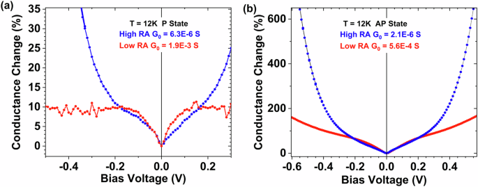
The bias-induced change in conductance for high (blue) and low (red; MTJ-H) RxA junctions in the (a) P and (b) AP states are shown. Initial inelastic tunneling is observed for both junction types up to |V | < 0.1 V. The (low) conductance of the high RxA junction strongly increases for |V | > 0.3 V due to the F center17,36, while the (high) conductance for the low RxA junction remains constant in the P state, and only moderately increases in the AP state. This highlights the near absence of F centers in low RxA MTJs.
To examine the energy extent of these states, we consider (hat{I})(V, T1,T2) = [{I(V, T2)/I(V, T1)}-1], i.e. the impact on I(V) of increasing temperature by ΔT = T2-T117,19,46. At V0, (hat{I})(V0) > 0 reflects how the additional thermal energy ΔkBT generates new transport channels thanks to states located ΔeV0 from EF within kB(T2-T1). Figure 3 depicts (hat{I})(V, T2) plots with ΔT = 80 K acquired on a MTJ-H MTJ. For both P and AP, an (hat{I}) peak centered at V = 0 indicates thermally activated inelastic processes (magnons, localized states, etc…). Beyond this peak, ÎP(V) is negative while (hat{I})AP(V) is positive, as expected from the R(T) data of Fig. 1.
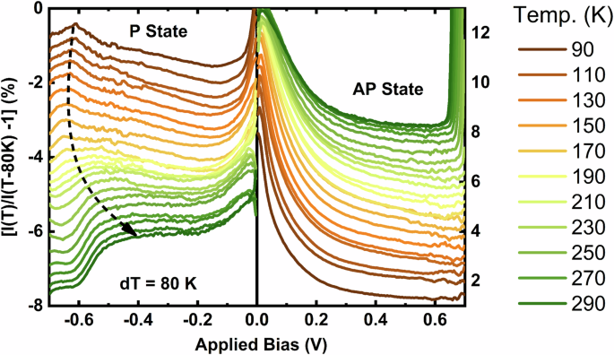
(hat{I}) plot for the MTJ-H’s (left) P and (right) AP magnetic states. Beyond a weak localization/inelastic transport regime at very low bias, thermally activated transport in the P state is metallic due to a band of states that extends 400 meV from EF at 290 K. Additional states appear beyond 400 mV. No such band is found in the MTJ AP state. The P state curves have been shifted for clarity.
In the P state, against this (hat{I}) < 0 background, we observe a (hat{I}) peak at 0.6 V and T = 90 K that shifts to 0.4 V at T = 300 K with increasing T. This peak is due to a change in the density of states at 0.4 eV away from EF in the barrier. We observe that (hat{I})P decreases to more negative values for |V | > 0.5 and T > 200 K. This plateau of non-zero, negative (hat{I})P amplitude suggests the presence of electronic states around EF whose thermally activated contribution to transport is complete by 200 K. No such features are found in the MTJ’s AP magnetic state (see Fig. 3). As we will see, this is because the enduring tunneling into the metallic counterelectrode due to mismatched electronic symmetries45,47,48 has a thermal activation that overshadows the presence of localized states. Similar (hat{I}) results were also obtained on MTJ-INL MTJs (data not shown).
It is known that the magnetic coupling between two FM layers can be altered by the presence of localized states in the tunneling spacer layer49,50. Since magnetic coupling is the steady-state outcome of spin-polarized currents across the trilayer, one may expect signatures of these localized states in STT experiments. In a first approach, we analyze the bias dependence of STT in nanopillar MTJ devices using spin-torque ferromagnetic resonance (ST-FMR)51,52. This technique probes the onset of magnetization dynamics that lead to STT thanks to an external microwave input (see Methods for details). We plot in Fig. 4a the resulting dc bias voltage as the microwave frequency is swept across the resonance condition, for several values of external bias. By fitting the data (see Methods), we obtain the bias dependence of the parallel and perpendicular torkance (see panels(b) and (c), respectively). The magnitude of the perpendicular torkance is nearly one order of magnitude lower than the parallel torkance, in agreement with previous reports53. Both STT parameters exhibit a marked change in trend at V = 400 mV, which matches the spectroscopic signatures of localized states seen in(,hat{I})P data (see Fig. 3). Note that the corresponding current density is 10x lower than the auto-oscillations threshold current, so that non linearity effects can be discarded here 54.
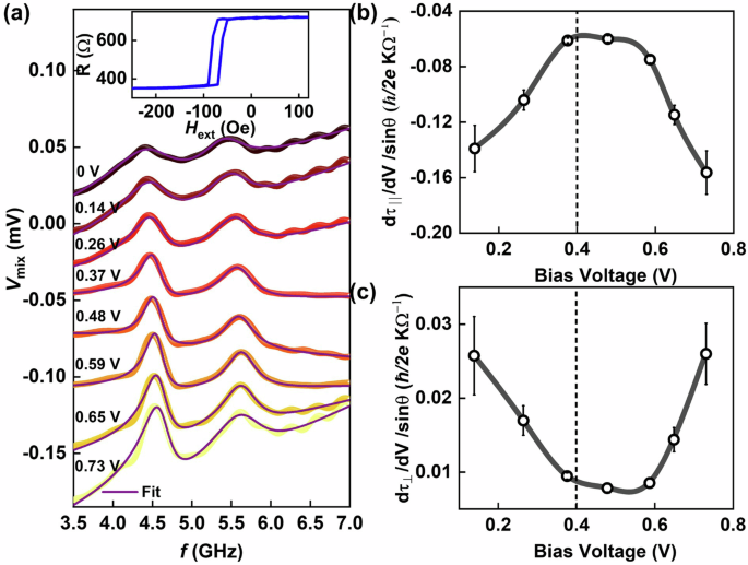
a ST-FMR spectra at 300 K on a MTJ-INL device for different bias voltages at (theta =185^{circ}) and Hext = 400 Oe. The inset shows magnetoresistance (MR) measured at 100 µA. The bias dependence of (b) parallel and (c) perpendicular torkance obtained from fits to the data of (a) change trends at 400 mV.
A complementary approach is to examine experimental deviations from a barrier-agnostic model55 of the critical current density JC leading to the STT effect:
Here, (alpha) is the effective damping constant, ({M}_{S}) is the saturation magnetization, ({t}_{F}) is the free layer thickness, ({H}_{K}) is the effective anisotropy field including magneto crystalline anisotropy and shape anisotropy, ({H}_{{ext}}) is the external field, and η = (P⁄2)⁄(1 + P2cosθ) is the spin-transfer efficiency (a function of spin polarization P and the angle (θ) between the electrode magnetizations).
We plot in Fig. 5aJC(T) for the P → AP and AP → P transitions. Within 25 < T(K) < 300, JC decreases by a factor of ~2 for P → AP, and by ~30 for AP → P. No temperature dependence of FeCoB properties (MS or HK) can explain either 1) the huge change in the AP state or 2) that this decrease strongly depend on the MTJ’s P/AP state. Note in particular the 10x reduction in JCAP→P within 250 < T < (K) < 300, even as JCP→AP decreases by ~0.5. We also find that the thermal activation coefficient of JC is 10x higher for AP → P compared to P → AP (data not shown). Finally, we plot the experimental and analytical temperature dependencies of ({J}_{C}^{Pto {AP}}/{J}_{C}^{{AP}to P}(T)) in Fig. 5b. We observe opposite trends and a clear deviation at high temperature.
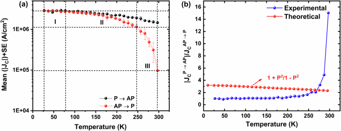
a Temperature dependence of JC for P → AP (black) and AP → P (red) STT switching. A MTJ-INL device was used. b Experimental and analytical temperature dependencies of ({J}_{C}^{Pto {AP}}/{J}_{C}^{{AP}to P},(T)).
Discussion
Low RxA MTJs now reach a lateral size of 2 nm43, and enjoy a broad range of communications10,11,12 and energy8,13,14,56 applications, yet understanding the actual nanotransport path37,39 across these devices has remained elusive. With this goal in mind, we infer the following facts from our bias-and temperature dependent magnetotransport data, our ST-FMR data and our STT critical current data presented above, obtained on low RxA MTJs and compared with high RxA MTJs:
-
1.
Low RxA MgO MTJs owe their much higher conductance to a much-increased density of double oxygen vacancies (M centers) at the expense of single oxygen vacancies (F centers). This is consistent with a prior report demonstrating that switching from ac sputtered MgO to dc sputtered Mg + oxidation – which is also used to form low RxA MTJs51,52,54,57,58,59,60, increases the ratio of double to single oxygen vacancies 19.
-
2.
Low RxA MgO MTJs are metallic in the P state due to in-gap states that span EF and extend up to 0.4 eV. These states aren’t visible in the ÎAP thermal activation spectroscopy. Since it is improbable that a mere P ↔ AP switching of ferromagnetic electrode alignment would extinguish these in-gap states, we infer that transport also proceeds onto these mid-gap states in the MTJ AP state, but that its thermal activation is overshadowed by that of enduring tunneling in the counterelectrode due to mismatched electron spin/symmetry29,45,47,48 (within 200 mV, the change in ÎAP ~ 6x ÎP for T2 = 90 K, see Fig. 3). This would explain the absence of a spectral signature in ÎAP.
-
3.
Low RxA MgO MTJs exhibit critical currents toward STT whose temperature dependence cannot be explained by ferromagnetic electrode properties alone.
We point out that the (hat{I})P and ST-FMR spectroscopies carry the signature36 at 400 meV from EF of the M* double oxygen vacancy (see Figs. 3 and 4b, c). Its thermal activation is dominant in the 250 < T(K) < 300 temperature range36, in agreement with the (hat{I})P data (see Fig. 3), and with the ×10 decrease in the JCAP→P(T) data (see Fig. 5a). Due to its Δ1 character19,28, transport in the MTJ’s AP state across the M* center would lead to semiconducting transport due to electron spin/symmetry mismatch in the MTJ counterlectrode. However, the M* center’s density of states does not intersect the Fermi level of a FeCoB/MgO/FeCoB MTJ 28,36.
An isolated F center generates states 0.7 eV from EF in a FeCoB/MgO/FeCoB MTJ28,36,38. Two F centers, when brought together as a M center form an anti-bonding state 0.4 eV from EF. We propose that, in low RxA MTJs, the localized states that cross EF and generate spectral weight at 0.4 eV from EF arise from anti-bonding states of higher energy due to an oxygen vacancy complex comprised of more than two oxygen vacancies17,19,28,36,37,40. Put differently, low RxA MTJs should have a comparatively higher density of oxygen vacancies than even moderately high RxA MTJs in which M centers dominate19. This picture is consistent with the decrease in F center weight as the RxA product is decreased (see Fig. 2).
To test this premise, and inspired by the phenomenological ‘pinhole’ description of defect-mediated transport across MTJs, we performed ab-initio calculations of the electronic properties of a Fe/MgO(5 ML)/Fe MTJ in which an oxygen vacancy complex composed of a zig-zag chain of oxygen vacancies that spans the MgO barrier has been inserted (see Fig. 6a and Methods for details). We first observe that, in the defect free-case (panel b), metal-induced gap states (MIGS) appear on the first two ML away from each interface, but promote no DOS at EF on the 3rd, central MgO layer. We thus dispel the commonly bandied argument that MIGS are responsible for metallic conduction in low RxA MTJs with 5 ML or more of MgO. In contrast, the oxygen vacancy complex we’ve considered, by virtue of antibonding states with a higher energy than those of a M center, does indeed generate a DOS on the MgO 3rd ML that spans EF. This validates our premise. We naturally refrain from explicitly ascribing our experimental data to this particular oxygen vacancy complex, but do note certain spectroscopic resemblances, such as the increase in DOS for E-EF < −0.6 eV (compare the 3rd MgO ML data of Fig. 6c with the (hat{I})P data of Fig. 3 and the ST-FMR data of Fig. 4b and c, keeping in mind the 0.25 eV Fermi level shift when going from Fe to FeCoB36). This candidate also leads to a TMR of ~100%, in broad agreement with experiments. Other oxygen vacancy complex candidates may theoretically yield similar features, but our experimental spectra around EF are broadened by other effects (e.g. magnon generation) that prevent a more precise discrimination between these theoretical candidates.
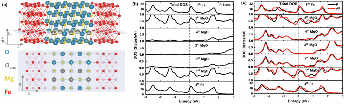
a Schematic of the zig-zag chain of oxygen vacancies in 5 ML f.c.c. MgO(001) spanning the bcc Fe(001) electrodes. Density of states calculated for a Fe(MLs 1-4)/MgO(5 ML)/Fe(MLs 5-7) MTJ, with (b) intrinsic/defect-free MgO, and (c) a zig-zag chain of oxygen vacancies that spans the MgO layer (a). In (c), the P (black) and AP (red) cases are distinguished. In the ideal MTJ, MIGS promote DOS at EF on the first two MgO MLs away from Fe, but not on the central MgO layer. This prerequisite toward metallic conduction is fulfilled by the zig-zag chain of oxygen vacancies complex, as a possible candidate.
To resolve basic contradictions between the conceptual understanding of spin-transfer torque across MgO and experiments on key spintronic green nanotechnology components, we have measured magnetotransport and ST-FMR on low RxA MTJs from two fablines, and compared results with those obtained on high RxA junctions. We attribute the anomalous metallic conductance in the low RxA MTJ’s P state to the presence of an oxygen vacancy complex formed of more than two oxygen vacancies. Its density of states spans the Fermi level, and derives from the double oxygen vacancy, which accounts for experimental spectral features in magnetotransport and ST-FMR, and in the thermal dependence of the spin-transfer torque critical current. Ab-initio calculations confirm that a zig-zag chain of oxygen vacancies that spans the MgO barrier constitutes a possible candidate for this oxygen vacancy complex.
Our work adds MgO MTJs to the burgeoning list of oxide electronic devices whose operation is defect-mediated. This paradigm of oxygen vacancy-driven spin-transfer torque has implications on how small a MgO MTJ can be laterally19,43,61,62, with an ultimate lateral limit around 7-8 ML MgO19, i.e. close to the present 2 nm experimental node43. This paradigm also opens new perspectives8,63,64 on utilizing the oxygen vacancy’s properties (e.g. optical absorption) toward additional device functionalities. Mastering oxygen vacancies in industrial MTJs could enable their dual-use not only as memory devices, but also as energy harvesters of ambient heat13,14,56. These are examples of using this technological platform, with controlled discrete electronic states, as a vector to industrialize quantum physics65. This paradigm of oxygen vacancy-enabled electronic device operation, using the ‘simple’ MgO oxide, should more broadly inspire the oxide electronics community as it goes nanoscale2 to implement ‘more than Moore’ concepts.
Methods
MTJ fabrication
The low RxA stacks nanopillar devices were grown and fabricated using fablines at TDK-Headway Inc. USA (labeled MTJ-H) and International Iberian Nanotechnology Laboratory (INL; labeled MTJ-INL), Portugal, respectively51,52,54,57,58,59,60. Details of the MTJ-H nanopillar devices are kept confidential by TDK-Headway Inc. USA. The MTJ-H nanopillar devices feature out-of-plane magnetic anisotropy, whereas MTJ-INL nanopillar devices features in-plane magnetic anisotropy. The nanopillar MTJ-INL devices were processed from the following stack: Al2O3(100)/Ta(3)/CuN(30)/Ta(5)/Pt38Mn62(17)/CoFe30(2)/Ru(0.85)/CoFe40B20(2.6)/MgO(wedge =0.6-0.9 nm)/CoFe40B20(1.4)/Ru(10)/Cu(150)/Ru(30) (all numbers in nm)54. A typical MTJ-INL device had an elliptical shape with a major (minor) axis of 250 (150) nm and TMR at 293 K (13 K) was 136% (235%). Its RxA product in P (AP) state was 26.71 Ω.µm2 (63.22 Ω.µm2) at 293 K and 26.20 Ω.µm2 (88.37 Ω.µm2) at 13 K. To obtain the temperature dependence of the critical current density (JC) for STT switching, a small magnetic field of 42 Oe was applied to compensate the stray field produced by the bottom electrode to ensure both P and AP states are maintained individually over the temperature range 10 < T(K) < 300. At a given temperature, each reversal was repeatedly measured, such that a mean JC and its standard deviation were extracted.
To make high RxA MTJs, Ta(5)/Co(10)/IrMn(7.5)/FeCoB(4)/MgO(2.5)/FeCoB(4.5)/Ta(5)/Pt(5) samples were sputter-grown at the Institute Jean Lamour (Nancy) on Corning 1737 glass substrates. MgO was ac sputtered in a pure Ar partial pressure. All numbers inside parentheses are in nanometers. Stacks were post-annealed in an in-plane magnetic field of 200 Oe for 1 h at 300 0C to both crystallize the MgO barrier and pin the lower electrode, thanks to the IrMn synthetic antiferromagnetic (SAF) layer. Samples were then processed within the STNano technological platform by optical lithography into 20 µm-diameter junctions with a typical RxA = 6 ×10⁷ Ω.μm2. Typical TMR values are 105% (200%) at 300 K (10 K).
ST-FMR measurements
ST-FMR measurements were performed on 220 nm-diameter MTJ-INL devices with a RxA product in the MTJ P (AP) state of 13.11 Ω.µm2 (27.59 Ω.µm2) at room temperature. The direction of equilibrium magnetization of the reference layer is taken along the positive x -axis with (theta =0^{circ}), where (theta) is the in-plane field angle. The AP state is obtained at H = 0. We used the radio frequency current modulation spin-torque ferromagnetic resonance (RFM-STFMR) technique: a rf current Irf.cos(2π.f).t was modulated onto a reference signal of 98 Hz and fed to the MTJ. A dc current (Idc) was simultaneously applied across the MTJ using a bias-tee. The output voltage (Vmix) is measured across the MTJ by using a lock-in amplifier by sweeping the frequency of Irf signal. We observe two distinct modes, and used the lower frequency mode with higher intensity to calculate torkance 66.
The detected voltage(,{V}_{{rm{mix}}}(f)) is given by:
Where, (C=,frac{1}{4},frac{{partial }^{2}V}{partial {I}^{2}},{I}_{{rm{rf}}}^{2}) is the non-resonant background signal. (S(f)=frac{1}{1+{(f-{f}_{r})}^{2}/{sigma }_{r}^{2}}) is the symmetric Lorentzian and (A(f),=,frac{(f,-,{f}_{r})/{sigma }_{r}}{1+{(f-{f}_{r})}^{2}/{sigma }_{r}^{2}}) is the antisymmetric Lorentzian. σr is the spectral linewidth (changes with bias current), and fr and f are the resonance frequency and microwave signal frequencies, respectively. Multiple modes were fitted using additional Lorentzian functions. The amplitudes of Lorentzian function, VS and VA depend on the derivative of spin-torque (i.e. torkance) as 67:
and
where ({{rm{M}}}_{{rm{s}}}) = 1.36 × 10⁶ A/m is the saturation magnetization, (d{tau }_{parallel }/{dV}) is the parallel torkance, and (d{tau }_{perp }/{dV}) is the perpendicular torkance, ({Omega }_{perp }={rm{gamma }}left(4{rm{pi }}{{rm{M}}}_{{rm{eff}}}+{{rm{H}}}_{{rm{ext}}}right)/2{rm{pi }}{{rm{f}}}_{{rm{r}}}) with (4{rm{pi }}{{rm{M}}}_{{rm{eff}}}) effective magnetic anisotropy, Hext = 400 Oe is the external magnetic field applied during the measurement, and fr = 4.53 GHz is the resonance frequency of the lower frequency mode. The value of the Irf is calculated by measuring the S11 parameter using a vector network analyzer (VNA)68. ({I}_{{rm{rf}}}=sqrt{frac{{2P}_{{rm{rf}}}left(1-{R}_{f}right)}{{R}_{{rm{dc}}}}}), with ({{R}_{f}=10}^{{S}_{11}/10}). In the present case, the reflection was found to be 10% within a frequency range of (2–10) GHz.


Responses