Phase change computational sensor

Introduction
Much of the information we perceive about the external world comes in the form of real-valued signals, and is conveyed through sensory organs. These organs perform data pre-processing such as signal filtration, compression, amplification, and digitization1,2,3,4. For example, neural circuits in the cochlea (retina) and cortex leverage non-volatile plasticity in synapses to pre-process auditory (visual) sequences, in order to enable subsequent down-streamed computations in the brain1,5,6,7. This observation suggests that emerging brain-inspired non-Von Neumann hardware concepts8,9 could enhance compute efficiency (in terms of energy and latency) and data privacy by incorporating ‘processing’ capabilities within sensor units. Recent progress has demonstrated processing within sensors using three-terminal photodiodes based on 2D materials10,11,12. These leverage the modulation of the photoresponsivities of pixels using field-effect. The first category of devices use an active gate terminal signal. Therefore, the compute feature is lost when the gate signal is removed. The volatility, therefore, necessitates buffers for storage of model weights (thereby strictly following the von Neumann architecture). In more recent demonstrations, charge-trapping effects have been proposed to program the photoresponsivities. While benefiting from non-volatility, this approach is more generally challenged by poor cyclability and high voltage requirements13. One promising approach can be decoupling the sensing and compute elements within the commercialized image pixel unit, while still maintaining dense integration. Such an approach can enable more manufacturable computational sensors for certain in-sensor-in-memory processing tasks (see Fig. 1a).

a An illustration of various on-system sensors in an autonomous vehicle. The sensors, including the vision cameras provide a means for the vehicle to perceive the surrounding environment. The camera comprises an active pixel array arranged in a crossbar topology. The pixels convert photons into an analog electrical signal. In the contemporary digital engine, the signal is then converted into binary streams and transferred to a digital von-Neumann unit where it is processed and recorded. In the proposed analog in-sensor engine, the pixels comprise non-volatile phase change memory devices. The output of the array evolves in accordance with the conductance states of the memory devices. A select configuration of the conductance states provides a means to perform a select computation directly on the input sensory signal. This signal can then be input seamlessly to a computational memory unit comprised of phase change memory devices for downstream in-memory processing. Symbols used in the diagram follow standard conventions for components. For example, the triangle represents the on-chip amplifier, the trapezoidal shape denotes the ADCs, and rectangles with arrows indicate the PCM devices. b A schematic showing an n × 4 pixel array. To perform 2 × 2 convolutions, as indicated by the blue-colored boxes, the select pixels are engaged (i.e., closed switches) to the bit lines and word lines, alongside select phase-change memory devices. The output representing multiply and accumulate operation is accumulated and passed on as activations for further processing to a multi-tile phase change computational memory. In effect, the sensor unit acts as an additional compute unit (that performs in-sensor compute, ISC) for the computational memory (that performs in-memory compute, IMC).
Here, we propose a computational sensor that utilizes embedded phase-change memory8,9 (PCM). Key idea behind our approach is that two-terminal non-volatile memory technologies, such as PCM can be readily integrated at the back-end-of-the-line with commercial sensors. Indeed, circuits using conductive ReRAM devices within image sensors have been proposed for tasks such as spike generations and averaging14, dynamic background subtraction15, image recording16, adaptive dynamic range modulation17, among others. Broadly, in these applications, the conductance states of the devices are either fixed (in enabling reference thresholds)14,15, or they dynamically and incrementally evolve during exposure to the stimuli signal16,17,18. An application where memristive devices are pre-programmed to select states within active sensor units to enable real-time visual inference remains to be demonstrated. Here, we consider an image sensor that incorporates PCM computational memory devices within its19,20,21,22 active m × n pixel array to perform dot product operations for in-sensor visual inference. The PCM devices are pre-programmed in an analog manner to execute scalar multiplication operation on the photo-generated current, thereby transforming the pixel output into an effective computational result. The accumulation step, which involves adding products from multiple pixels, is achieved by summing the output of neighboring pixels—which are determined by the kernel size—in parallel along the interconnects of the sensor’s crossbar. Hence, as a k × k kernel traverses a segment of the pixel array (see Fig. 1b), the corresponding (m, n) pixels can be read out, and their values accumulated as output signals. Consequently, the sensor generates an image that represents a pre-computed version of the raw input. This output can be further downstreamed to the PCM computational memory cores for subsequent processing, as has been previously suggested with other memristive-type memories23,24,25,26,27.
Pixel Characteristics
A PCM device integrated into the sensor’s active pixel provides a signal division in the output (see Fig. 2a(i)), obeying ({v}_{m,n}={v}_{mo,no}times (frac{{D}_{m,n}}{{D}_{m,n}+{G}_{m,n(kappa )}})). Here, vm,n is the output of the Pm,n pixel in the array. Gm,n(κ) is the conductance value programmed into the kth PCM device of a pixel and Dm,n is the conductance of the pixel, that scales with the input signal ϕ. vmo,no is the PCM device independent output of the pixel. Crucially, the expression suggests that for a fixed input, vm,n increases with decreasing Gm,n(κ), and for a fixed Gm,n, it increases with increasing amplitude of ϕ. The device characteristics can be collectively represented using load lines (RL). The figure (see Fig. 2a(ii)) shows a simulated current-voltage characteristics of a pixel under increasing light flux (ϕ1→5), and decreasing Gm,n (RL1→5). The plot illustrates that by modulating Gm,n, it becomes possible to configure a selection of sensitivity and dynamic range to light detection at the individual pixel level. For instance, in bright environmental conditions, a large dynamic range can be achieved to avoid pixel saturation (at the expense of sensitivity) using high Gm,n, while under dark conditions, high sensitivity can be enabled for faint signal detection (at the expense of dynamic range) using small Gm,n.
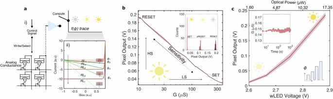
a (i) A sketch illustrating the operation of a single pixel. The pixel is connected to mushroom-type phase-change memory cells. Control signals are instructions for selecting and programming the memory devices. A selected device modulates the pixel depending on its conductance state. (ii) Calculated current-voltage traces of a photodiode to illustrate that the memory devices provide a means to constructing reconfigurable and virtual load lines (RLn) that affect the pixel’s dynamic range and selectivity under varying illumination (ϕi) conditions. Each load line state encodes a unique non-volatile phase configuration of memory device as conceptually sketched in the insets. b A plot illustrating the characteristic curve of a computational sensor pixel. The graphs show the variation in the pixel output in accordance with the conductance state of the memory device, under a constant illumination condition. The inset is a histogram plot highlighting a pixel’s output for three programmed non-volatile conductance states. c A plot illustrating the pixel’s output for a constant conductance state under increasing illumination. The inset shows a pixel’s output vs time plot under constant illumination conditions.
In our toy demonstration, a pixel is comprised by isolated components: a protoytype circuit board that hosts the phototransistor circuitry, and a silicon chip containing isolated PCM devices (in supporting information section S1, the setup and a SPICE simulation of the circuity is shown). The PCM device is of the contemporary mushroom-type and utilizes 80 nm thin film of Ge2Sb2Te5 (or GST) phase-change material. During read-out under illumination, the state of the PCM device modulates the output. Programming the state involves write operations, specifically electrical current pulses that induce Joule heating for the amorphization (RESET) and crystallization (SET) of the phase-change material within the PCM device. A PCM device can be programmed to various non-volatile conductance states by adjusting the amplitude of the programming pulses. Figure 2b demonstrates the dependency of the output signal of a pixel on the conductance state of the PCM device. The experiment is conducted under constant illumination, and the measurement is repeated 10 times in this plot. The plot validates the configurable sensitivities of the phototransistor through the phase configuration of the PCM device. The diode can be persistently tuned to high sensitivity (HS) by programming to the RESET states within a PCM device and to low sensitivity (LS) by programming to the SET states. Furthermore, the extent of this tunability can be significant, constrained only by the memory window (GSet − GReset) of the PCM device (in our measurements, a conductance compliance of 10 μS reduces this range by an order of magnitude, to ~ 30x).
Thus, a computational sensor unit enables optimal detection of changing environmental conditions via non-volatile modulations of the conductance states of the PCM devices, as is highlighted in the inset of Fig. 2b. In this experiment, we performed pixel reads 1800 times for three conductance states of the PCM device (SET, partial RESET, RESET) to demonstrate the sensor’s adaptability in responding to varying brightness conditions. In Fig. 2c, we showcase the scalability of the sensor’s output under different illumination conditions. In this measurement, the PCM device is configured to the SET state. The output exhibits a proportional increase with illumination intensity, attributed to the rising photocurrent generated in the diode (the measurement is repeated 10 times). Given the expected low noise in the SET state of PCM devices, this measurement suggests that the spread in the output is primarily influenced by peripheral components on the circuit board. In the inset of Fig. 2c, we plot the sensor’s output immediately after programming its PCM device to a partial RESET state. The measurement extends over 1500 s and illustrates the stable nature of the output signal. This stability is attributed to two factors: the signal divider read-out scheme (as opposed to the standard current read-out in which conductance drift becomes prominent) and the pseudo-projection28 rendered by the conductance-limiting component in the pixel.
In-sensor convolutions
A prominent class of computational models that stands to gain from in-sensor computations are convolutional operations. Images can be blurred, sharpened, or embossed for standalone use cases with convolutions or prepared in real-time as formatted/pre-processed inputs for deep computing networks (see Fig. 3a), such as in convolutional neural networks (CNNs). In a convolution operation between an image of dimension n × n and a filter of dimension k × k, the number of MAC (multiply and accumulate) operations required to process the image, scales as (n−k)2. When n > > k, which is a typical case (e.g., 1280 × 1024 pixels sensor using 16 × 16 canonical filters29), the compute becomes very expensive. Therefore, one approach toward an efficient hardware can be to divide the computational effort between the sensor and the processor (see Fig. 3a–b). That is, by performing convolutions as when the data is captured using in-sensor computing, convolution operations of the first layer can be offloaded from the processor. As an example, with data gathered from our experimental setup, in Fig. 3c we simulate in-sensor convolutions for an image blurring operation. Image blurring (or smoothing), provides a point-spread capacity by reducing the amount of noise and speckles in the input, and is a common pre-processing task.
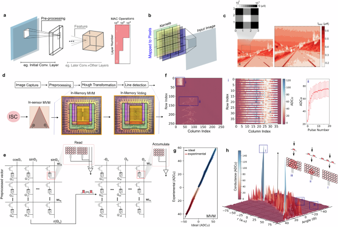
a An illustration of a computer vision model. An image is processed by this model which comprises preprocessing and subsequent feature extraction steps. The number of operations scales with the depth of the network as is shown for a LeNet-5 model, i.e., the first layer that computes directly on the input image is computationally most demanding. b An illustration showing the direct computation of the convolutions during image sensing by leveraging the crossbar topology of the active pixel array. c An illustration of emulated Gaussian blurring of an input image as a preprocessing step. d The Hough transformation pipeline is illustrated, where in-sensor computations preprocess images to generate inputs for computational memory tiles. Computational memory performs MVM and accumulation operations to detect lines in the images. e In the first operation, the input image is converted into a vector that is multiplied by a matrix encoding the parametric space transformation. The resulting output becomes the input for the accumulator space. In this space, select PCM devices experience an increase in their conductance values based on the number of times they are programmed by the input. f The experimental plot depicts a computational memory tile, showcasing the encoded regions for MVM and accumulation operations. The MVM region is programmed only once, while the accumulation operation involves all devices being reset. Over time, the mapping in the accumulation operation evolves based on the number of input pulses they receive. ADCu stands for analog-to-digital conversion units. g An experimental MVM plot displays the measured output of the computational memory. The black trace represents the ideal result from floating-point MVM. h A 3D plot illustrating the accumulator space after the computational memory has preprocessed an input image. Two unit-cells, representing a unique (r, θ) tuple, underwent the largest increase in conductance.
Additionally, depending on the circuit design, the accumulations can be made either on the image sensor array (MACSensor), which is the mode discussed so far, or on the word lines of a PCM computational memory array (MACPCM-tile) (in supporting information section S2, illustrations of these configurations are shown). In either case, we note that the most optimal scenario for in-sensor convolutions is when s ≥ k, where s is the fixed stride that defines the number of pixel shifts of the kernel between subsequent MAC operations. This constraint has two benefits: (i) convolutional operations on all pixels in select rows can be carried out in parallel, reducing the computational complexity to O(c) (or O(fc) with f filters) under MACSensor where c(k, s) < m, and (ii) the number of PCM devices can be kept to a minimum within each pixel. For the case s = k, the number of PCM devices in a pixel scales with f, thus simplifying the integration and arbitration schemes. In contrast, when s < k, the kernels overlap, leading to the loss of parallelization (owing to requirement to toggle between different kernel values in the overlapping regions). Such overlaps also create disproportionate number of PCM devices per pixel. For example, considering s = 1, the number of PCM devices in an mth, nth pixel follow f ⋅ k2 for mth ≥ k − 1 and nth ≤ n − k − 1. Nonetheless, it is worth noting that since n > > k is a typical condition, the constraint s = k may not be a limitation —the resolution of the output or the quality of the image transformation can be reasonably preserved.
Model-based learning
Beyond contemporary CNNs, convolutional operations remain crucial in model-based vision. An instance of this need arises in tasks like model-based object recognition, where the types and instances of a set of objects in a given scene are known beforehand. As an illustration, we delve into the example of lane/line detection in an image using Hough transformation30. The computational workflow involves image preprocessing (conducted through in-sensor convolutions, using the framework discussed earlier) followed by the downstream task of Hough transformation performed in the computational memory (see Fig. 3d). To showcase this, we utilize the IBM HERMES Project Chip, fabricated using 14 nm complementary metal-oxide-semiconductor technology31, featuring a 256 × 256 crossbar array of PCM unit cells.
The transformation converts each point (x, y) in the image to the parameter space coordinate (r, θ) using the expression (overrightarrow{r}=xcos (theta )+ysin (theta )), where r is the distance from the origin to the closest point on the straight line, and θ is the quantized angle between the x axis and (overrightarrow{r}), representing the line in the image. This operation is succeeded by a voting procedure in the accumulator space. The coordinates (cells) with the highest counts in the parameter space signify the most likely parameters describing a shape (in supporting information section S3 a more comprehensive discussion about implementation of Hough transformation is discussed). As an initial step, we adapt these transformations for in-memory computations. This can be accomplished using in-memory matrix-vector multiplications (MVMs) for the parametric space and conductance accumulations to implement the accumulator space. Interestingly, the same task utilizes the two—and otherwise disparately used- computational primitives for PCM devices: scalar multiplication computations from the multilevel conductance values and the accumulative behavior arising from crystallization dynamics32,33. In the MVM, columns of the crossbar array are assigned θn values, such that m × n PCM devices can encode fixed values for cos(θn) and sin(θn). This way, parallel Multiply and Accumulate (MAC) operations are performed on the inputs, and the outputs represent the r(θ) values. The accumulator operation is then performed in a computational memory array whose elements are represented by the (θ, r) tuples. In this accumulation scheme, all cells are initialized in the RESET state. The cell’s conductance evolves according to the number of constant amplitude crystallization pulses, and the computation result is stored in place due to PCM’s non-volatility. By reading out the PCM devices with the highest conductance values using a threshold scheme, the most likely lines are extracted, and their approximate geometric definitions are determined. In Fig. 3e, these operations are illustrated. Both MVM and accumulation operations are carried out in the same computational memory array, leveraging non-overlapping areas. Figure 3f(i) illustrates the matrix encoding the trigonometric values, and Fig. 3f(ii) shows an example of conductance change from pulse accumulations. Figure 3g shows MVM results performed for 82 points in an input image. The results of MVM are then used to locate the (θ, r) pairs for the accumulation operations, as illustrated in Fig. 3h. Starting in the RESET state, different devices attain different conductance values after processing the entire image. The most conductive devices encode the correct angles the lines subtend.
Discussion
Processing data, quasi-locally, i.e., in the edge, has traditionally required substantial processing power, memory, and communication bandwidth. One of the key ideas we propose is to implement the convolutional operations within the sensor: in particular, the initial layer of the computing networks. Under the typical rolling shutter scheme, when performing the convolutional operations, k rows in the sensor are read-out in parallel. For s = k, the read-out time of a single frame becomes ({T}_{R}=frac{{t}_{{rm{R}}}}{mtimes s}), where tR is the digitization of a single row. Therefore, larger-sized kernels inherently improve the frame rate of the sensor. However, it appears that this improvement is only valid for the case f ≤ s. Since f depends on the application, this improvement metric must be considered application specific. An added gain also appears from the reduction in the data volume that must transferred to the memory or processor. This is because an image of dimension m × n, undergoes dimension reduction (m − k + 1) × (n − k + 1) from convolutions. We also discuss approaches to speed-up model based approaches, all the while by leveraging the crossbar topologies of the sensor and computational memory units. As an exemplar problem, we discuss Hough transformation based object detection model. We discuss how, by embedding this model, into the proposed approach, the time complexity34 (O(N4)) can be reduced to a constant O(c), where c < < N (in supporting information section S3 we estimate the time complexities). It is also worth noting that in-sensor computations can benefit standalone imaging sensors, by providing the pixel’s a means to adapt to varying lighting conditions. Since this occurs at low power expense owing to the non-volatility of the PCM devices, the battery lives of sensors, such as hand-held devices can be extended. Although our concept can be applied to other non-volatile memory technologies, we believe PCM holds the most promise for computational sensors. PCM is at a very high maturity level of development and has been commercialized as both standalone memory and embedded memory8,35,36. This fact, together with the ease of embedding PCM on logic platforms make this technology of unique interest31,37.
We identify the following limiting cases in which in-sensor computations are expected to accelerate processing. When applied to shallower networks (eg. single or few user-defined filters), when applied to downsampled images (smaller m values) in deep networks, when s number of filters are offloaded from the processor to the sensor, and when applied to certain preprocessing tasks for machine learning. In supporting information section S4, we have estimated the performance gains (areal, energy and latency gains) by emulating the implementation of convolutions on ISC-IMC. Some important challenges, however, must be pointed out. To avoid read disturbance of PCM devices, the output voltage range must be kept below the threshold voltages of the phase configurations. When considering scaling up, that is the integration of PCM with stacked CMOS sensor chips, interconnects and their connectivity will become an important factor. This could, altogether, necessitate novel integration methods, including hybrid bonding38 (i.e, physical stacking of wafers). In summary, we make a proposal for a computational sensor that combines the contemporary phase-change memory technology with contemporary sensors to enable in-sensor-in-memory computing for edge intelligence.
Methods
Electrical characterization
The devices for optoelectronic measurements comprised an 80 nm thick film of a GST phase-change material, sandwiched between bottom and top metal-nitride electrodes, where the bottom electrode radius was 20 nm. The IBM HERMES Project Chip comprised similar mushroom-type devices but with doped-GST phase-change material. See reference31 for more information about the chip. The electrical measurements were performed in a custom-built probe station. DC measurements of the device state and biasing of the optoelectronic circuitry were performed with a Keithley 2600 System SourceMeter. AC signals were applied to the device and the white LED for illumination with an Agilent 81150 A pulse function arbitrary generator. A Tektronix oscilloscope (DPO5104) recorded the voltage pulses applied to and transmitted by the device and the LED. For read-out and programming of the pixel unit, switching between the circuit for DC and AC measurements was achieved with mechanical relays. See Supporting Information Section 1 for more information about the measurement circuitry.
Responses